Note: Descriptions are shown in the official language in which they were submitted.
CA 02428187 2003-05-07
Method of Fabricating Sub-micron Structures in Transparent Dielectric
Materials
Field of the Invention
This invention relates to the field of microstructure fabrication, and in
particular to a
method of fabricating sub-micron structures in transparent dielectric
materials.
Background of Invention
There is a need to integrate materials with optical waveguides for both
sensing
applications as well as a means to alter the properties of the propagating
light. The
integration can include, for example, biological and chemical samples,
polymers, liquid
crystals as well as non-linear optical and modulator materials. Such
integration can
benefit from the manufacture of dense arrays of sub-micron wide, high aspect
ratio holes
(with attoliter volumes; I attoliter = 10-18 liters)or channels in dielectric
materials, such as
glass which are interfaced directly with adjoining optical waveguides for
light delivery
and light detection with the holes or channels.
There is also a need to fabricate 2-D and 3-D photonic crystal structures such
as arrays of
closely spaced holes in glass to assist in light guidance. Such structures
might be used, for
example, to construct compact turning mirrors for integrated photonic
circuits.
Optical components, such as variable optical attenuators or all optical
switches, may also
be based upon the integration of holes/channels and optical waveguides. Also,
there is a
need to fabricate narrow wires to electrically connect integrated photonic
devices and to
fabricate miniature integrated RLC electrical circuit components in a
dielectric chip.
There is also a need to form miniature electrodes for biological screening
applications.
-1-
CA 02428187 2003-05-07
The fabrication of holes or channels in transparent dielectrics can currently
be
accomplished using various drilling techniques such as Focused Ion Beam (FIB)
and high
peak power laser ablation. One example of the latter technique is described in
the paper
"Three-dimensional hole drilling of silica glass from the rear surface with
femtosecond
laser pulses" (Opt.Lett.,26,pp. 1912-1914,2001). The authors of this paper
claim to have
produced high aspect ratio holes with diameters as small as 4 pun using water
to assist in
removing ablation debris.
Recently femtosecond laser pulses have been used to modify special UV
sensitive
photomachinable glass which when combined with chemical etching
(Y.Kondo,J.Qiu,T.Mitsuyu,K.Hirao and T.Yoko,Jpn.J.Phys.38,pp.LL1146-1148,1999)
can be used to make 10 m diameter holes. The paper entitled "Femtosecond
laser-
assisted three-dimensional microfabrication in silica"( A. Marcinkevicius et
al,Opt.Lett.26,pp.277-279,2001) describes the use of a very high NA (1.3) oil
immersion
microscope objective to create a column of small micron cubed damage volumes
(voxels)
in silica which when etched creates a hole or channel with much larger
diameter (10pun)
than the diffraction limited laser spot size (1 m). This occurs since the
etching rate in the
highly damaged zone is much higher than in the unmodified zones. This creates
a long
narrow hole which can act as a reservoir to trap acid to permit lateral
etching to occur at
the same time and at the same rate over the entire length of the hole opening
up the hole
in a uniform manner. The "voxels" are highly damaged zones of modified silica
and
cannot be used to form low loss optical waveguides. There is no evidence to
suggest that
sub-micron holes or channels can be made in this way. The use of such high NA
objectives also severely restricts the distance between the lens and the
irradiated zone
(e.g. a few hundred microns).
-2-
CA 02428187 2003-05-07
US Patent No. 5,919,607 describes the use of light absorption in boron doped
glass
together with chemical etching to produce large channels and other large
structures.
Microfabrication techniques, such as Reactive Ion Etching (RIE) use mask, ion
beam and
etching technologies to make precise holes or channels in glass. It is
possible to use
microfabrication techniques to construct optical waveguides with adjoining
channels
fabricated into the surface of dielectric materials. The fabrication of a
waveguide that
extends from the surface deep into the substrate is difficult to accomplish
with
conventional microfabrication techniques.
There are self-organization techniques, e.g. using colloidal particles, as
well as
microfabrication techniques, which can be used to make 2-D photonic crystal
structures
(H-B Sun, Y.Xu, S. Matsuo and H. Misawa, Optical Rev.,, 6, pp. 396-398, 1999).
It is believed that no-one has successfully made a practical 2-D photonic
crystal band gap
structure for telecom wavelengths in bulk glass with any of the above
techniques. The
construction of 3-D photonic band-gap structures is considerably more
difficult and has
met with limited success. The concept of using femtosecond lasers to fabricate
holes to
form a 2-D photonic crystal structure band-gap structure has been described in
US patent
No. 6,134,369,Date of Patent Oct.17,2000. However, methods on how to make the
holes
were not discussed.
One way to make a variable optical attenuator is to use a temperature
sensitive, absorbing
polymer as a cladding layer in an optical waveguide. A controlled heat source
can be used
to vary the temperature of the polymer and therefore the attenuation. The
waveguide core
can be reduced in size in the vicinity of the polymer in order to force more
of the
waveguide mode into the cladding region to enhance attenuation. An optical
switch can
-3-
CA 02428187 2003-05-07
be constructed based upon the attenuator design and switching the heat source
on and off
on top of the polymer.
Microfabrication techniques could also be used to construct an all optical
switch based
upon three coupled waveguides in which the central waveguide contains a doped
core
(e.g. Erbium) which when optically pumped (e.g. at 980 nrn) produces gain at
telecom
wavelengths which promotes the switching of near-infrared light from one
outside guide
to the other outside guide as proposed by F.Di Pasquale and E.Hernandez-
Figueroa
IEEE J. Quantum Electron., 30, pp.1254-1258, 1994).
Mask and various metal coating techniques are currently used to micro
fabricate fine
wires as well as RLC circuit elements and electrodes into a dielectric.
State of the art laser drilling or laser induced dielectric modification
followed by chemical
etching techniques have not been able to produce clean, deep, sub-micron wide
holes or
channels in transparent dielectric materials. Hole diameters are generally >4
m and are
rough. It has also not been possible to make an adjoining waveguide to the
channel or
hole.
Microfabri cation can be used to make a number of devices incorporating the
integration
of materials with optical waveguides. However microfabrication is best suited
to making
large quantities of a single device. It requires access to sophisticated
laboratories, which
are not always available and are costly to setup. The production of numerous
different
devices with modest product volumes can benefit from alternative manufacturing
techniques such as those based upon computer controlled laser writing. Laser
writing is
very flexible and can adapt quickly to new designs, leading to rapid
prototyping. Laser
-4-
CA 02428187 2003-05-07
writing techniques operate under ambient conditions and are easier to
integrate with other
manufacturing processes.
Summary of Invention
According to the present invention there is provided a method of fabricating a
microstructure in a transparent dielectric material, comprising focusing
femtosecond laser
pulses into said dielectric at a sufficient peak laser power, intensity, and
laser dosage to
create a highly tapered modified zone having a length: width ratio > 4:1 with
modified
etch properties, said tapered modified zone having at least one tip with a
diameter less
than about 250 nm; and selectively etching into said modified zone.
The modified structure can be in the form of a single conical structure with a
base, in
which case the diameter of the base is typically greater than about 1 gm, or
it can be in
the form of a double conical structure with tips extending outwardly from a
central base
region, or region of maximum diameter, which typically has a diameter in the
order of
600nm. In the case of the double conical structure the tips typically have a
diameter of
about I OOnm. The double conical structure is useful for producing narrow
shallow holes
near the top surface of the dielectric material.
The laser pulses can be generated with a single laser or multiple lasers. In
the latter case
multiple laser beams can be combined to generate the pulses and permit the
field
distribution in the focal volume of said laser beams to be changed so as to
vary the shape
of said modified zone.
Alternatively, an aspherical lens element(s) can be included in said laser
beam to change
the field distribution in the focal volume of said laser beam to vary the
shape of said
modified zone.
5
CA 02428187 2003-05-07
The state of polarization of the laser can be unpolarized or linear and with
the plane of
polarization being rapidly rotated.
A microstructure typically has channels with sub-micron diameters, although
the
diameters could extend into the micron range, and, for example, be several
microns. An
important advantage of the invention, however, is that it is capable of
creating structures
with sub-micron lateral dimensions but with depths of microns.
A femtosecond is 10-15 seconds. A femtosecond laser generates pulses in the
femtosecond range. The femtosecond laser used by the inventors typically had a
pulse
duration of 30- 40 femtoseconds. However, similar performance for fabricating
microstructures can be anticipated for pulse durations on either side of this
value e.g. 20
fsto150fs.
The laser beam can be fixed relative to the sample. In this case, the laser
dosage is the
product of the energy per pulse times the number of pulses delivered to the
modified
zone. It is typically varied in the range determined by altering the energy
per laser pulse
from 0.01 to 3 J and the number of shots between 500 and 5000.
Alternatively, the beam can be displaced relative to the sample. In this case,
where the
sample is scanned as it is being irradiated, dosage refers to the cumulative
energy per
micron of translation and is the product of the energy/pulse times the
repetition rate of the
laser and divided by the scan rate. The dosage in typically varies in the
range determined
by the energy per pulse from 0.01 to 10 ;the repetition rate from 10-250 kHz
and the
scan rate from I0-200 m/s.
Preferably, the tapered modified zone is located inside the material so that
the laser
intensity near the surface is too low to modify the surface, and etching takes
place from
-6-
CA 02428187 2003-05-07
the tip of the tapered zone so that as said selective etching proceeds
longitudinally into
said modified region, the progressively increasing width of said tapered zone
compensates for lateral etching occurring at said narrow end. However, a
tapered zone
near the top surface can be used in certain applications, for example, in
microfluidic
applications, to create tapered holes, for use, for example, as nozzles.
The invention is based in part on the discovery that the amplified femtosecond
laser
pulses appropriately focused into a dielectric material create a conical zone
of modified
material having sufficient length, taper angle and degree of material
modification such
that when the conical structure is placed near the bottom surface of the bulk
dielectric (i.e.
the narrow tip region of the conical structure is near the bottom surface) and
chemically
etched, it produces steep sidewall, sub-micron wide holes or channels.
The method in accordance with the invention allows sub-micron structures to be
created
in dielectrics, such as glass. The method takes advantage of the highly
tapered shape of
the modified zone induced in the dielectric material by the focused amplified
femtosecond laser pulses. When a series of high repetition rate (10-250 kHz),
for
example, Ti:sapphire femtosecond laser pulses (? = 800 nm) with power levels
above a
threshold value (approximately 1 x10⁶ W) are appropriately focused (with e.g.
a NA=0.7
microscope objective) into a silica glass block, the modified zone, which is
much smaller
in width and of different symmetry than that would be expected using
conventional
optical formulas, is produced.
[]It is possible to produce modified zones that have upper and lower portions
directed
away from a central wider portion terminating in respective tips. In this
case, the wider
portion is considered the base of the modified zone.
7
CA 02428187 2003-05-07
A second novel aspect of the invention is the use of the femmtosecond laser
modified
regions adjoining the channels as waveguides to couple light into or out of
the channels.
This is made possible since the modified regions are uniform in composition
and can
provide low loss light propagation. Furthermore by retracting the focused
laser beam
from the bottom surface, it is possible to both modify the dielectric near the
surface to
produce a hole after chemical etching, and also create a waveguide directly on
top of the
hole. This waveguide can be written in the bulk material to a desired location
well away
from the hole.
The combination of a channel sitting on top of an adjoining waveguide, which
is a feature
of this invention, can be used to make telecom devices such as a variable
optical
attenuator. It may also be possible to insert other materials into the
channels to function as
modulators of the light carried just below the channel.
The capability of producing dense arrays of small sub-micron holes in glass
can be useful
in constructing 2D photonic crystal band-gap structures to enable the
fabrication of
compact waveguides. The freedom and flexibility of an automated laser writing
technique
combined with the simplicity of chemical etching provides some advantages over
a
microfab solution. There is an added advantage if the same femtosecond laser
that
creates the modified structures can also be used to write optical waveguides
to interface
with the etched photonic crystal structures.
The ability to produce narrow holes or channels on silica wafers could have
application in
the field of micro fluidics as a means of achieving a high density of channels
containing
very small volumes of fluid.
-8-
CA 02428187 2003-05-07
The coexistence of an optical waveguide above a hole or a channel can have
sensor-on-a-
chip applications, e.g. in the biological sciences. For example, a series of
holes
terminating in waveguides can serve as attoliter receptacles for biological or
chemical
samples, which can be irradiated with light of a particular wavelength. Light
emitted from
the samples can then be carried away by the waveguides coupled to the
respective holes
for spectral analysis. A horizontal channel adjoining a horizontal waveguide
can also be
used for a similar purpose. Fluid can flow through the channel, and light
emitted can be
carried away by the adjoining waveguide for spectral analysis. Of course, the
system
could also operate in reverse with the waveguide subjecting the sample to
intense light in
order to determine its response.
According to a further aspect of the invention there is provided a method of
making an
electro-optical modulator comprising firing femtosecond laser pulses into a
bulk dielectric
to create a tapered zone with modified etch properties; translating the focus
of said laser
pulses through said bulk dielectric; selectively etching into said tapered
zone to create a
main channel; filling said main channel with electro-optical material; firing
femtosecond
laser pulses into said bulk dielectric on either side of said main channel to
create a tapered
zone with modified etch properties; translating the focus of said laser pulses
on either side
of said main channel; selectively etching into said tapered zones on either
side of said
main channel to create side channels; and filling said side channels with
metal.
The invention still further provides a method of making a method of making an
all optical
switch, comprising temporarily bonding together first and second dielectric
components;
applying femtosecond laser pulses to said first component near an interface
between said
components to create a tapered modified zone with modified etch properties;
translating
the focus of the laser pulses; creating alignment marks on the second
component;
-9-
CA 02428187 2003-05-07
separating said first and second components; etching the bottom of the first
component to
create a channel with an adjoining waveguide therein; partially filling said
channel with
refractive material; applying femtosecond laser pulses to said second
component near a
surface thereof to create tapered zones with modified etch properties;
translating the focus
of the laser pulses; etching the bottom of the second component to create a
channel with
an adjoining waveguide therein; at least partially filling said channels with
refractive
material; and recombining said first and second components with their
respective
channels aligned.
Brief Description of Drawings
The invention will now be described in more detail, by way of example only,
with
reference to the accompanying drawings, in which:-
Figure 1 (a) is a schematic illustration showing a cross-sectional view of a
modified zone
in a glass dielectric;
Figure 1 (b) is a schematic illustration of three important growth stages of
the modified
zones with increasing femtosecond laser dosage;
Figure 2(a) illustrates how a modified zone selectively chemically etches to
form a hole
from the tip side of the conical structure;
Figure 2(b ) illustrates how a modified zone selectively chemically etches to
form a hole
from the base side of the conical structure;
Figure 2(c) illustrates the steps in the fabrication of a channel with
adjoining waveguide
in a glass block when etching is done from the side of the base of the conical
structure;
-10-
CA 02428187 2003-05-07
Figure 2(d) illustrates the situation in a glass block when the etching is
done from the tip
side of the conical structure;
Figure 3(a) is a SEM image of femtosecond written selectively chemically
etched holes in
silica glass;
Figure 3(b) is a SEM image of a hole produced using a NA=0.45 microscope
objective to
focus the femtosecond laser light;
Figure 4 is an AFM image of an etched femtosecond laser induced channel;
Figures 5a to 5c are schematic illustrations of a variable optical attenuator;
Figure 6 illustrates the steps in making an electro-optic modulator;
Figure 7 illustrates the steps in the fabrication of an all optical switch;
and
Figures 8a to 8c show the steps in the fabrication of a dynamic polarization
mode
dispersion compensator in a fiber.
Detailed Description of the Preferred Embodiments
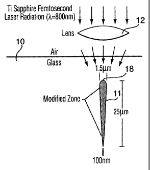
In accordance with the principles of the invention, as shown in Figure l a, a
series of high
repetition rate (10-250 kHz) Ti:sapphire (X=800 nm ) femtosecond laser pulses
with
power levels above a threshold value (approximately 1 x 10⁶ W) were focused
into a
silica glass block 10 through focusing lens 12 (e.g. an NA -0.7 microscope
objective ).
This creates a highly tapered (length: width > 8:1) modified zone 11 much
smaller in
width and of different symmetry (Fig.1(a)) than that expected from
conventional optical
formulas. The tapered zone 11 is in the form of an inverted cone with a base
at the top
having a diameter of 1.0 to 3 pm. The cone has very smooth steep sides. The
inventors
have found surprisingly that the tip at the bottom has a diameter in the order
of 100nm,
-11-
CA 02428187 2003-05-07
and typically less than about 250nm. This is a remarkable result because the
tip size is
considerably less than the wavelength of the light, typically in the order of
X/8. It is
believed that the inventors" measurements are the first to reveal the extreme
sharpness of
these long (>15 m) conical structures.
There are three basic stages to the growth of the conical structures with
increasing laser
exposure as depicted in Figure 1(b). Stage I is typical of low energy dosage
irradiation
but with peak laser powers above the threshold for material modification. The
conical
structure is narrow (600nm) and short (8 m) and tapers in both directions to
sharp tips in
a symmetrical fashion. At higher dosages the structure grows both upwards
towards the
input laser beam and downwards into an elongated taper (stage II).The width of
the
structure also increases .With further increase in dosage the top half of the
conical
structure tends to square-off and has typically x2 greater modification than
the bottom
portion which continues to taper to a fine tip (stage III ). This shape does
not change too
much as the laser dosage is increased further. However, the top portion of the
conical
structure begins to show signs of damage.
Similar uniform conical structures and stages of growth development have been
observed
using Boron doped glass (BK7) at similar but lower laser dosages. However in
this case it
is preferable to use low laser repetition rates (e.g. 10 kHz) to form the
conical structures,
when one uses J laser pulse energies, to avoid serious thermal damage to the
modified
structure.
The modified zones described above 11 are very uniform and have a higher index
of
refraction, than the surrounding material 10. The magnitude of the index of
refraction
difference is sufficient (An-- 0.004) to form an optical waveguide. As just
mentioned the
-12-
CA 02428187 2003-05-07
induced index of refraction in the top part of the inverted cone (stage III)
i.e. near its base,
can be approximately 2x higher than in the narrow part near the tip. However,
the index
of refraction profile down the length of and across the tapered region is
remarkably
constant. There are no signs of damage processes or the formation cavities
occurring in
the tapered region. The transition from unmodified to modified material is
extremely
sharp (<100 rim), indicating a high degree of non-linearity to the
modification process.
The induced index of refraction saturates at higher laser energy per pulse
resulting in very
reproducible modified zones insensitive to pulse-to-pulse variations in the
laser
parameters.
The inventors have discovered that the modified zone etches faster relative to
the
unmodified material in buffered oxide etchant (10:1 BOE), although
hydrofluoric acid
(HF) can also be used.
Figures la, lb, 2a, and 2b show the effects of firing femtosecond lasers
pulses at a single
location. Figures 2(c) and (d) show the effects of translating the focus of
the pulses
laterally through the bulk dielectric.
If the femtosecond laser beam is focused through the top surface of a
dielectric with a
dosage to produce a stage I shaped conical structure and if the dielectric is
etched from
the top surface, the etching process tries to open up a hole laterally However
the
increasing size of the conical structure at greater depth compensates for the
lateral etching
to produce a cylindrical hole.
However, if the femtosecond laser beam is focused through the top surface of a
dielectric
with sufficient dosage to create either a stage II or stage III shaped conical
structure 11
(as shown in Fig. I (b)) just below the top surface, and if the dielectric
material is etched
-13-
CA 02428187 2003-05-07
from the top surface, the etching process results in a hole which exceeds the
diameter of
the base of the cone. As etching proceeds the tapered modified zone will act
to produce a
strongly tapered hole rather than a cylindrical hole. This is shown in Fig.2b.
Such highly
tapered holes are of limited use for 2-D photonic crystal applications and are
non-ideal for
most other applications. They can, however, find application in microfluidic
applications,
for example, to form nozzles.
In Figure 2(c), the focus of the laser beam is translated so that the
successive tapered
zones 11 produce a wedge-shaped modified zone 15. If this structure is etched
from the
top, a V-shaped groove 16 connected to a wedge-shaped waveguide 17 is formed.
In the case of top etching, there is also risk of disruption to the uniformity
of the modified
region if the focused laser beam at the surface is of sufficient intensity to
cause surface
damage. It has also been observed that laser beams focused just below the top
surface (a
few pm) can modify the material back to the top surface. This occurs without
any
catastrophic surface damage, but in such a manner that it is very difficult to
uniformly and
efficiently etch the dielectric material covering the desired modified region.
In the preferred embodiment of the invention, the laser writing procedure
involves
focusing the laser beam deep enough inside the material so that the laser
intensity near the
top surface is too low to modify the surface. The top of the modified zone
should be at
least 20 gin below the top surface. The material should be etched from the
bottom
surface. It is preferable to position the tip of the conical structure just
above the bottom
surface, preferably a few microns above the bottom surface, so as to minimize
the
thickness of material to be etched. This results in better selective etching
of the modified
region. In cases where the sample thickness exceeds the working distance of
the
-14-
CA 02428187 2003-05-07
focusing optics the tip of the conical structure will have to be positioned at
a known
distance from the sample surfaces and the sample can either be cut and
polished or just
polished to put the bottom surface close to the conical tip.
The etchant acts on the "narrow tip" region first which it tries to open both
in the direction
of the conical structure and laterally into the unmodified material. As the
etching
proceeds the emergence of the progressively wider modified zone compensates
for the
lateral etching to produce a hole (in the case of a static laser) or channel
18, which has
generally straight sidewalls as shown schematically in Fig.2(a) and Fig.2
(d))respectively. The channel adjoins region 19 having modified etch and
refractive index
properties and which serves as a waveguide adjoining the channel 18.
The narrow width of the tapered region of the conical shaped modified zone
makes it
possible to produce holes or channels 18 having a width as small as 300 nm in
undoped
silica glass. The inventors have also demonstrated that two sub-micron wide
holes can be
produced as close as 1.4 m apart, opening up the possibility of creating very
high hole
densities. Fig.3(a) shows an SEM image of part of a 5x5 array of some of
discrete holes
that have been made in the static case, i.e. without translation of the laser
pulses. The
holes are clean and appear to have steep sidewalls. The channel in the
translation case has
a width approximately equal to the diameter of the holes.
For stage I weakly modified conical structures which show tapering on the top
as well as
on the bottom of the conical structure (Fig. I (b)) some compensation for the
lateral
etching will be provided when etching from the top surface although only for
shallow
holes.
-15-
CA 02428187 2003-05-07
Approximately 4000 shots at z 750 nJ/shot were needed to modify the glass for
each hole.
It is therefore possible to make arrays of such holes in minutes. When the
laser beam is
translated parallel to the bottom surface it has been found that the
accumulated energy
dosage (i.e. energy per pulse times the number of pulses) delivered to the
dielectric
material per micron of translation needs to be about 10-5 to 10-2 Joules.
In order to make deep (> 2 m), sub-micron diameter holes, which might be of
interest
for 2-D and 3-D photonic crystal applications, the laser dosage must be chosen
to provide
sufficient material modification in the tapered region to obtain a high degree
of selective
etching. The numerical aperture (NA) of the focusing optics can also be chosen
to provide
sufficient taper length (a lower NA will result in a longer conical taper) to
be able to
produce both a deep and narrow hole after etching. Typically the NA used is
about 0.7,
however very nice sub-micron wide holes can be made, for example, using an
NA=0.45
lens as shown in Fig. 3(b). The use of modest NA long working distance
focusing optics
also permits large samples (cms) to be used and still be able to focus to the
bottom
surface. It becomes progressively more difficult to produce a long (>5 p.m)
uniform
undamaged highly tapered zone as the numerical aperture of the lens increases
beyond
0.9.
The taper angle of the conical structure must be sufficiently large to
compensate for the
lateral etching in order to make steep sidewall holes. However the rate of
lateral etching
will depend inversely on the rate of selective chemical etching i.e. greater
selective
etching in the modified zone will result in less lateral etching for a given
hole depth. It is
therefore important to achieve highly selective etching. The dielectric
material can be
doped or chosen from a number of multicomponent glasses of from photosensitive
glasses
to increase the degree of material modification and/or to permit more rapid
etching
-16-
CA 02428187 2003-05-07
relative to the unmodified region. This will result in narrower deeper holes.
A thick doped
layer (e.g. 20-30 gm) or component glass or photosensitive glass layer can
also be
deposited onto the bottom of say silica glass to achieve the same purpose.
The holes can be made at various angles with respect to the bottom surface by
adjusting
the angle of incidence of the conical structure.
It is also possible to increase the laser dosage in selected locations to
create easy to etch
holes/slots to serve as reservoirs for the acid to enter into the bulk
material to permit
etching of conical structures, which are e.g. parallel to the bottom surface.
In this way
holes or channels can be created along three orthogonal axes. This is a
necessary feature
to make complicated 3-D photonic crystal structures.
If the focus of the femtosecond laser beam is translated close to and parallel
to the bottom
surface of a silica wafer sample, for example, it is possible to produce a
narrow sub-
micron channel with steep sidewalls after etching as shown in Fig. 4. If the
etching
process is stopped before entering into the top part of the cone, then the
remaining
modified structure can act as a waveguide with glass surrounding the core on
all sides
except one which is normally air (Fig.2 (d)). Another medium can be put in the
channel
18 provided it has an index of refraction lower than that of the glass and
that it assists in
guiding light.
If the irradiated zone had been near the top surface of the dielectric sample
then the
waveguide left after etching would include the narrower sub-micron tapered
region and
would not be as satisfactory for light propagation (Fig.2 (b)).
The width of the waveguide adjoining the channel is ~l .7 m, which is
satisfactory for
the propagation of visible light but not near-infrared light (i.e. for
core/clad index of
-17-
CA 02428187 2003-05-07
refraction differences :S 0.01). Two or more side-by-side conical structures
are required to
sweep out a larger waveguide width to transmit X=1.5 m light. These
structures are
formed side-by-side at each location prior to translation of the focus of the
laser pulses
laterally through the material, i.e. in a direction perpendicular to the
direction of the
translation direction of the laser pulses. The number of side-by-side zones
can be adjusted
to create tapered channels or waveguides. A wider more symmetric waveguide can
also
be produced using aspherical optics (e.g. combination of a microscope
objective an
angled (with respect to the scan angle) cylindrical lens) as shown in
international
application published under the Patent Cooperation Treaty (PCT) WO
02/16070A2.2002
entitled "Methods for creating optical structures in dielectrics using
controlled energy
deposition" by O.L.Bourne, D.M. Raynor, P.B.Corkum, M.Mehendale, and A.
Naumov.
The waveguide shown in Fig.2 (d) is a very special waveguide since it
automatically
tracks the etched channel, which can of course be formed into complicated
patterns. Light
can be evanescently coupled from the waveguide into the channel 18 which could
contain
various liquids or biological materials for spectroscopic analysis. The
evanescent
coupling of light into the channel is very sensitive to the index of
refraction of the
material and can be used as a means of determining its value.
The etched channel can partially filled with a polymer, a thermo-optical
material, a metal,
biological material, fluids or other substances which can affect the
propagation. An
example for a very straightforward application of the channel and adjoining
waveguide is
as an index of refraction monitor for fluids. The transmission of light down
the
waveguide will be strongly influenced by the index of the fluid cladding
layer.
-18-
CA 02428187 2003-05-07
Instead of translating the focus of the femtosecond laser beam along the
bottom surface,
the beam can be moved vertically within the material toward the top surface.
The sample
can then be chemically etched from the bottom surface to produce a small hole
with an
optical waveguide sitting right on top of it. Furthermore, the focused laser
beam can be
raster scanned to produce a larger modified zone resulting in a larger
diameter hole (e.g.
10-20 gm). Of course this technique can be used to produce dense arrays of
such holes
each with its own waveguide.
The conical structure shown in stage I of Fig. 1(b) can be written with its
sharp lower tip
approximately 10 m from the bottom surface. When the femtosecond. laser beam
is
translated parallel to the bottom surface (or the sample translated) it
produces a
waveguiding structure. At various locations during the translation the laser
dosage can be
increased producing a structure shown as stage III in Fig. 1(b).The tip of
this extended
structure would be just above the bottom surface. It is also possible to
withdraw the laser
beam vertically off the surface to create a vertical waveguide.
After chemical etching a series of channels and/or holes will be created in
the heavily
dosed regions while no channel/holes will be produced in the low dosage
regions. This
procedure results in a series of holes adjoining a horizontal waveguide and
attached if
desired to a series of vertical waveguides. It provides the capability of
simultaneously
delivering light via the horizontal waveguide to all the holes or holes. Light
emitted from
material in the holes can then be detected using each vertical guide above the
holes.
In order to make precise holes and channels it is necessary to keep the
focused laser beam
the same distance above the bottom surface as the sample is translated. This
can be
achieved in a number of ways including optically imaging the emerging plasma
as the
-19-
CA 02428187 2003-05-07
laser beam just penetrates the bottom surface; creating a small laser damage
spot on the
bottom surface with the femtosecond laser (The reflected femtosecond laser
signal from
the spot can be used to set the distance of the lens to the bottom surface);
using a lens to
focus a collimated femtosecond laser beam onto the bottom surface of the
sample and
adjusting the lens to surface distance to keep the back-reflected beam also
collimated
(When the collimated beam is focused n to a CCD it will result in the minimum
spot
size); and interferometry.
The above methods are not restricted to glass but can also apply to other
materials such as
sol gels and transparent or semi-transparent polymers. In the case of polymers
chemical
etching with acids such as HF would be replaced with appropriate organic
solvents.
The structures described so far are structures that can be made from focusing
an
essentially Gaussian shaped femtosecond laser beam into a dielectric material.
It is also
possible to use various masks upstream of the focusing optics, or to combine
multiple
beams, or to use aspherical optics to modify the shape of the input beam
profile and to
optimize the shape of the modified region. Structures with precisely
controlled, sub-
micron separations can be made in this way.
In order to make smooth (structure variations < 100nm) walled channels it is
preferable to
use an unpolarized laser beam or to scramble a linear polarized beam by
rapidly (e.g.
10kHz) rotating the polarization direction.
The following examples show how various materials contained in the channels
and holes
can be integrated with the adjoining optical waveguides to perform useful
functions. The
examples also demonstrate how devices can be made which benefit from the
capability of
making precise structures in dielectrics.
-20-
CA 02428187 2003-05-07
Example 1. Fabrication of Photonic Components: A Variable Optical Attenuator
The combination of a channel with an adjoining waveguide can be used to
fabricate a
temperature controlled variable attenuator for telecom applications as shown
in Figures
5a to 5c. In this application a channel 20 created by femtosecond laser
writing followed
by selective chemical etching (Fig.5(b)) is partially filled with a polymer 21
(Fig.5(c))
whose index of refraction is less than that of the waveguide core and which
has a
temperature dependent absorption at e.g. 2=1.5 ..m. The polymer 21 could also
be from a
class of polymers with large thermo-optical responses leading to large index
of refraction
changes as the polymer is heated. The index gradients can be made sufficiently
large to
deflect light out of the waveguide.
A metal coating 22 is subsequently deposited on top of the polymer and the
entire surface
is polished to remove the metal and polymer everywhere except in the channels.
The
small cross-sectional area metal channel 22 serves as a resistive heating
element to adjust
the temperature of the polymer.
Light launched into the left side of the device experiences attenuation in the
top portions
of the waveguide containing the polymer cladding. In this case the channel 20
has been
written by focusing the femtosecond laser light through the bottom surface to
finish just
under the top surface. In the second half of the device the waveguide path can
be written
so that it is near the bottom surface (i.e. laser writing from the top) so
that the light
distribution at the bottom of the waveguide now experiences attenuation
producing an
overall symmetric attenuation of the waveguide mode. If the light distribution
entering
the device is asymmetric in the direction perpendicular to the base of the
polymer channel
then the controlled independent heating of the top and bottom polymer channels
can be
-21-
CA 02428187 2003-05-07
used to restore symmetry. Arrays of such variable attenuators can be made on a
single
silica chip. The attenuators can be made into a series of optical switches by
turning the
heating elements on and off on top of each polymer channel.
Example 2. Microfluidic Applications on a Silica Chip
The method in accordance with the invention permits the production of precise
channels,
which can be tapered and formed into complicated patterns such as mixing
chambers for
chemistry on a chip experiments.
The value of these narrow channels for chemistry on a chip experiments is
enhanced since
with each channel there is an adjoining optical waveguide, which can couple
light into or
out of the channel. One could also use arrays of micron-sized holes to trap
very small
droplets of liquid for analysis.
It is also possible to partially coat the interior of the channels/holes with
metal. The metal
is then removed everywhere except in the channels/holes by polishing. Laser
radiation
delivered through the waveguides attached to the channels/holes can be
absorbed by the
metal to control the temperature of samples placed in such channels/ holes.
The laser
radiation can also be used heat the samples sufficiently rapidly to eject the
material from
the holes.
Example 3. Biological Sensing Applications on a Chip
Very small volumes of biological material can be inserted into the narrow
channels
where it can be interrogated by light traveling in the waveguide adjoining the
channel.
There are also biological sensor applications for holes and their vertically
connected
waveguides. For example, biological specimens could be inserted into the
holes. An
-22-
CA 02428187 2003-05-07
entire array of holes could then be irradiated with UV light and the
fluorescence from
each specimen could be guided by its own waveguide for selective detection.
Alternatively holes containing a sample could be individually irradiated or
sampled
through its own waveguide.
It is also possible to use light traveling in a horizontal waveguide, which
has no adjoining
channel but instead interfaces with a series of holes, to simultaneously
irradiate material
contained in all of the holes. Light emanating from each hole e.g.
fluorescence, can be
detected using the dedicated vertical waveguides adjoining each hole.
Example 4. Insertion of Materials between Interconnected Waveguides for
Telecom
Applications
It will be appreciated that the method of the invention makes it possible to
create a hole
(Fig. 3) at the termination of a waveguide i.e. at the glass/air boundary. The
hole diameter
can have approximately the same dimensions as the waveguide. Arrays of such
waveguides can be written inside a block of dielectric and terminated in such
holes. The
holes can then be filled with material which could alter the intensity,
polarization or other
properties of the light propagating through the holes to interconnect with an
external set
of waveguides butted to the holes.
Example 5. Fabrication of Wires and Mirrors
This application takes advantage of the capability of producing smooth and
steep side-
wall channels or holes. If the etched channels 20 shown in Fig.5 (b) are
coated with just a
metal layer and then polished to remove the metal everywhere except in the
channels, it is
possible to make wires. The wires could be used to provide electrical
connections for
integrated optical components fabricated on the surface or just below the
surface into the
-23-
CA 02428187 2003-05-07
bulk glass. Metallization of the channels 20 followed by polishing can also be
used to
make electrodes for biological screening experiments.
Example 6. Fabrication of RLC Circuits and an Electro-optical Modulator on a
Dielectric
Chip
This application takes advantage of sub-micron resolution laser writing and
chemical
etching to make small components. When the interior of two parallel closely
separated
channels are coated with a metal and the metal is removed everywhere except in
the
channels they can act as a capacitive element. It is also possible to produce
oscillatory
variations to the channel pattern in the plane of the bottom surface of the
dielectric to
produce an inductive element. Control over the channel dimensions on a micron
scale
also permits the fabrication of resistive wire elements as discussed in
example 5. The
construction of miniature RLC components could be useful for detector arrays
or other
optical components on a dielectric chip.
An example of such a component is an electro-optical modulator. Such a
modulator could
be formed by putting an appropriate electro-optical material into a channel
sandwiched
between two conductive plates and applying an external voltage. This can be
accomplished using the following steps, which are shown schematically in Fig.
6:
1. The femtosecond laser plus selective chemical etching technique is used to
create a
channel 40 in a silica wafer 41 with cross-sectional dimensions typical of a
near-infrared
waveguide.
2. Electro-optical material 42 is deposited to fill the channel 40.
3. The wafer is polished to remove the electro-optical material 42 everywhere
except in
the channel 40.
-24-
CA 02428187 2003-05-07
4. The wafer is then overcoated with a thick layer of silica 43 (preferably
doped to
enhance selective chemical etching).
5. The femtosecond laser plus selective chemical etching technique is used to
create two
side channels 44 close to the channel filled with modulator material 42.
6. The wafer is metallized to fill the two side channels 44 with metal 45.
7. The wafer is polished to remove the metal 45 everywhere except in the two
channels.
Electrical connection can then be made to the side channels 44.
8. Femtosecond laser writing is used to produce waveguides 46 to connect to
either end of
the electro-optic waveguide.
Example 7. Fabrication of an All Optical Switch
The all optical switch consists of three parallel closely coupled waveguides
in which the
core of the central guide is doped with a gain medium such as erbium ( Er). As
understood by persons skilled in the art, an "all optical" switch is one in
which the
switching of light is controlled by light. When this waveguide is optically
pumped (e.g. at
980nm) it exhibits gain at telecom wavelengths. The gain results in the
controlled and
efficient switching of light from one outside guide to the other. The closely
coupled
waveguides can be fabricated using the method in accordance with the invention
and
according to the following steps, which are shown in Fig.7:Two blocks of glass
31, 32 are
temporarily bonded together. Femtosecond laser pulses are focused through the
bottom
surface of the lower block 32 to just below the interface between the blocks.
The
femtosecond laser can be scanned across the block to enlarge the modified zone
33 as
shown in Fig 7. The focused light is also allowed to just enter the base of
the second
-25-
CA 02428187 2003-05-07
block to mark the perimeter of the modified zone. This process is repeated at
various
locations to produce arrays of modified zones 33.
The blocks are then separated and the bottom block is chemically etched to
create a series
of channels each with its own optical waveguide adjoining it. The second block
31 can be
irradiated with femtosecond laser pulses in the marked regions to create
identical
modified zones and channels after etching.
The channels 34 are then partially filled with silica glass 35. Er-doped
(erbium) glass 36
is deposited into the remaining portion of the channel 34. The top layers of
Er-doped
glass and silica are then removed, e.g., by polishing, to produce a two
waveguide
structure.
The two blocks 31, 32 can be recombined as shown at step 5 and then aligned so
that the
sets of waveguides overlap. This produces the three waveguide geometry.
A silica layer 38 can be added after step #4 to produce a four element
waveguide structure
shown in Fig.7.
The above method of fabrication has the following advantages over using
femtosecond
laser pulses to directly write all the waveguides into a multilayered slab
containing an Er-
doped layer. Firstly, it is presently not clear whether it will be possible to
use
femtosecond laser pulses to write a high quality waveguide in highly doped Er-
glass.
Furthermore the spacing between all the waveguides is critical for switching
since it
determines the degree of evanescent coupling between the guides. Fabrication
with the
combined femtosecond laser irradiation and chemical etching produces
waveguides in
which the distance between the doped and undoped guides is determined by the
thickness
of the silica layer (i.e. step #2), which can be very accurately controlled.
-26-
CA 02428187 2003-05-07
It will be appreciated by one skilled in the art that the method in accordance
with the
invention is not restricted to use with blocks, slabs or wafers of dielectric.
material, but it
.also applicable to other geometries, such as fibers and capillary tubes. For
example, the
femtosecond laser beam could be focused from either side and down the length
of a
single-mode fiber to produce high index of refraction regions near the fiber
core defining
a preferential direction across the core to create a polarization maintaining
function. After
chemical etching, narrow slots or holes 50 could be produced radially like
spokes of a
wheel around the fiber core 51 as well as down the length of the fiber as
shown in Fig.8.
The narrow slots could be placed close to the fiber core and yet still be able
to define a
fairly precise radial direction. These structures could be filled with various
photonic
related materials such as the temperature sensitive absorbing or thermo-optic
polymers,
which were discussed in example 1. Metal coating of the fiber impregnated with
such
arrays of polymer channels would result in a fiber version of the variable
optical
attenuator described in example 1.
It is desirable to be able to control the temperature of the material in each
of the etched
channels. However, in the case of the fiber geometry, polishing the curved
surface to
remove the metal everywhere except in the channels is difficult. It will
probably be
necessary to use a technique such as femtosecond laser ablation to remove the
metal
between the slots.
These types of structures can also be used to make a dynamic polarization
dispersion
compensator for telecom fibers. Femtosecond written waveguides can be used as
multiple
taps to sample the light beam propagating down the fiber. This signal can be
analyzed by
a polarimeter to obtain polarization information on the light, which can be
sent to a
polarizing transformer to correct for polarization mode dispersion and
polarization
-27-
CA 02428187 2010-05-31
dependent loss. The femtosecond written and chemically etched conical
structures
described above and shown in Fig.8 (a) can be used to make such polarization
corrections. Arrays of etched channels 50 containing a thermo-optic polymer 52
covered
with a metal 53 to form a resistive element, which can be independently
heated, provide a
means of dynamically changing the index profile in the core/cladding region
(Fig. 8(b)).
It might also be possible to just use metal in the channels and depend on
local thermally
induced stress gradients to provide polarization mode dispersion compensation
(Fig.
8(c)).
The narrow channels described above can also be used to enhance a fiber's
sensitivity as a
strain or temperature sensor as described by Y.Jiang,S.Pang and Y.Cui, Proc.
of
SPIE,3491,pp. 897-901,1998.
There are also a number of possible applications which could utilize the high
density of
small diameter holes coupled to dedicated waveguides feature of the described
technique,
especially when the modified zone tapers in both directions so as to produce
generally
cylindrical holes in the dielectric material.
(1) Phosphors can be deposited into the holes for light conversion e.g.
infrared to visible.
(2) Some metal can be deposited into the holes. The holes are then filled with
biological
or chemical material and the light transmitted down the dedicated waveguide is
used to
heat the metal and therefore the sample in a controlled way. The sample could
also be
heated to the point where it is ejected from its micron sized hole onto a
receiving
template. Similar things can be done without the metal coating but would
require that the
sample strongly absorb the laser light.
-28-
CA 02428187 2003-05-07
(3) The use of the technique to make controlled distributions of small
diameter closely
spaced holes for photonic crystal applications e.g. to assist light in making
sharp turns.
(4) The top surface of a slab containing arrays of waveguides with bottom
surface holes
can be backlit and then the light emanating out of the hole precisely
indicates the position
of the hole to a vision system. Biological material can then be precisely
dropped onto the
hole. Conversely when a reader of optical information, e.g. fluorescence, from
the
sample, e.g. DNA, scans the surface the backlit hole will allow it to know it
is over the
biological specimen. This application is satisfying since it uses both the
small hole and
also the adjoining waveguide.
While many embodiments of the invention have been described by way of example,
it
will be appreciated by one skilled in the art that many other variations of
the invention are
possible within the scope of the appended claims.
-29-