Note: Descriptions are shown in the official language in which they were submitted.
CA 02428340 2003-05-09
79031-7
1
FLOOR MONITORING SYSTEM
FIELD OF THE INVENTION
The present invention relates to a system for monitoring the
identity of individuals stepping onto a floor surface and
movement of such individuals across the floor surface.
BACKGROUND OF THE INVENTION
Monitoring systems for tracking the movement of persons are
known.
For example, commonly owned pending Canadian Patent
Application No. 2,324,967 is directed to a system for
monitoring the location of an individual relative to one or
more detectors. The system uses a transmitter worn by a
person, which emits an identification signal which is picked
up by a detector located at a monitoring station. The
detectors are capable of identifying the particular
individual as well as their distance from the detector. Such
systems are limited in that they provide only the location
of the individual relative to the detector.
Floor monitoring systems are also known. The known floor
monitoring systems use pressure gauges to detect when weight
is placed on the floor.
SUMMARY OF THE INVENTION
According to a broad aspect of the invention there is
provided a floor monitoring tile comprising: a contact layer
having an upper surface and a lower surface, the lower
surface having a plurality of conductive contacts; a sensor
layer having a plurality of first conductors and a plurality
of second conductors, each first conductor having a
CA 02428340 2003-05-09
79031-7
2
plurality of first contact points and each second conductor
having a plurality of second contact points, for each
contact a respective first contact point of said first
plurality of contact points and a respective second contact
point of said second plurality of contact points forming a
set being aligned with the contact; wherein for each
contact, when no force is applied to the contact, the
respective first contact point and the respective second
contact point remain electrically isolated and when force is
applied to the contact, the respective first contact point
and the respective second contact point electrically connect
through the contact.
According to another aspect of the invention there is
provided a system for monitoring the movements of at least
one individual across a floor surface comprising: a
plurality of floor tiles; the floor tiles each having an
upper surface, a contact layer, a sensor layer and a
detector; the contact layer having a plurality of conductive
contacts; and the sensor layer comprising a plurality of
pairs of contact points which are electrically connected by
the conductive contacts of the contact layer when force is
applied normal to the contact points; wherein the detector
calculates an area of the floor tile over which the force is
applied as a function of time.
The present invention provides a monitoring and
identification system which is capable of tracking the
movement of individuals across a floor surface including the
measurement of their gait, speed, direction, footprint
geometry or volume and how each foot contacts the floor.
The monitoring system may also provide the person's identity
CA 02428340 2003-05-09
79031-7
3
and link their movement pattern to stored historical
information.
An advantage of the present invention in some embodiments is
that it provides significantly more information than
conventional monitoring systems.
BRIEF DESCRIPTION OF THE DRAWINGS
Embodiments of the present invention will be further
described with reference to the accompanying drawings,. in
which:
Figure 1 is a block diagram of a preferred embodiment of the
floor monitoring system of the present invention;
Figure 2 is an exploded view of a floor monitoring tile
according to a preferred embodiment of the present
invention;
Figure 3A is a cross sectional view of a portion of a
contact layer;
Figure 3B is a schematic plan view of a portion of a contact
layer;
Figure 3C is a schematic plan view of a portion of a sensor
layer of a preferred embodiment of the present invention;
Figure 4A is an electrical schematic of a portion of the
contact and sensor layers according to a preferred
embodiment of the present invention;
Figure 4B is an electrical schematic of a circuit which
results when a portion of the dimples depicted in Figure 4A
are depressed;
CA 02428340 2003-05-09
79031-7
4
Figure 4C is an electrical schematic of a circuit which
results when a conductor column depicted in Figure 4B is set
high;
Figure 5 is a block diagram of a quarter contact panel of a
floor tile according to a preferred embodiment of the
present invention;
Figure 6 is a block diagram of a central processing unit of
a floor tile according to a preferred embodiment of the
present invention.
DETAILED DESCRIPTION OF THE PREFERRED EMBODIMENTS
Conventional systems do not identify the individual's exact
location. They also do not provide information regarding
how the individual is moving across the floor surface
including gait, speed, direction, footprint geometry and how
each foot contacts the floor. In many applications it would
be useful to have detailed information about how a person is
moving. In medical applications, that information can be
used to assess the individual's progress towards recovery
from an illness. Equally, in security applications, the
information can be used to assess whether an individual is
engaged in prohibited activities. In scientific
applications, that information can be used to understand the
gait of animals such as horses and dogs.
Referring to Figure 1, a floor monitoring system generally
indicated by 10 is comprised of a plurality of floor tiles
12 (only four shown), a data bus and power supply 14 and a
central processing computer 16. The floor tiles 12 are
mechanically interconnected to form a floor surface. The
floor tiles are also electrically interconnected by the data
bus and power supply 14. The data bus and power supply 14
CA 02428340 2003-05-09
79031-7
interconnect both the floor tiles 12 to each other and to
the central processing computer 16. Each floor tile 12 also
has a unique identification which is communicated to its
nearest neighbour for configuration purposes.
5 The system also includes bracelets 18 and at least one
doorway sensor 20. The bracelets 18 are worn by the
individuals to be monitored. Instead of the bracelet 18, a
broach, necklace, other personal accessory, a swipe card or
an implant may be employed. In the case of a swipe card, the
doorway sensor 20 is replaced by a card reader.
Each of the bracelets 18 emits a unique identity signal,
preferably a radio frequency signal. Each bracelet 18 is
configured to allow the doorway sensor 20 to receive and
retransmit, to one of the floor tiles 12, the identity
signal of each bracelet 18 when it is within the range of
the doorway sensor 20. The range of the doorway sensor is
preferably at least one meter but other ranges can be
employed. The doorway sensor 20 does not necessarily need
to be positioned in a doorway and multiple doorway sensors
20 may be positioned around the floor surface. Preferably
the doorway sensor 20 is electrically connected to a floor
tile 12 which receives identity information and communicates
that information to the central processing computer 16.
In security applications, swipe cards can be used. The
floor tiles 12 are positioned before the card reader. When
the swipe card is read by the card reader, the information
registered by the floor tiles 12 is compared to historical
information. A card holder is permitted to advance only if
the data matches.
Although the bracelets 18 provide identity information, in
another embodiment, the floor monitoring system 10 operates
CA 02428340 2003-05-09
79031-7
6
without the use of the bracelets 18. The floor monitoring
system 10 will then provide information regarding the
movement of individuals but will not directly indicate the
identity of the individual being tracked although it may be
possible to derive the individual's identity based on the
information provided by the floor tiles 12. The central
processing computer 16 will determine the identity of the
individual using the signals generated by the floor tiles.
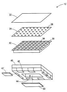
Figure 2 depicts the various layers which make up each floor
tile 12. The layers of the tiles consist of a surface layer
22, contact layer 24, sensor layer 32 and tile base 40.
Preferably, the floor tiles 12 have an area of two feet by
two feet and a thickness of two centimetres or less but more
generally any suitable dimensions can be employed. The
surface layer 22 is the upper surface of the tile with which
an individual's feet may contact. An alternative embodiment
of the invention would allow the floor tiles 12 to be
assembled without the surface layer 22 and a sheet of
flooring to be laid over the entire surface of all of the
floor tiles 12 of the floor surface. However, the preferred
embodiment of this invention provides complete individual
floor tiles 12 with the individual surface layer 22. The
material used for the surface layer 22 must readily flex
when stepped on but must spring back to its original shape
when weight is removed from the layer. The preferred
material identified for this aspect of the invention is
styrene butadiene rubber which is also known as synthetic
rubber. This material flexes and quickly returns to its
original shape when repeatedly loaded by footprints. The
material used for the contact surface also preferably allows
for the application of labelling, is not damaged by
cleaning, is wear-resistant, slip-resistant and comfortable
to the sense of touch.
CA 02428340 2003-05-09
79031-7
7
The next layer is the contact layer 24 which has a plurality
of dimples 26 defined therein which are used to form
contacts. Means other than dimples may also be used to form
the contacts. The dimples 26 are preferably on a grid of
128 by 128 resulting in a total number of dimples of 16,384
dimples 26 per each floor tile 12. The dimples 26 are shown
in further detail in cross-section in Figure 3A. Figure 3A
shows that each dimple 26 has vertically angled sides 30 and
a contact area 28. Preferably, the contact layer 24 is
comprised of thermal formable foam compound and in
particular polyolefin which is known for sub-flooring
applications. The contact areas 28 are formed on the bottom
side of the contact layer 24. Preferably, the contact areas
28 comprise resistive paint, which is sprayed onto the
dimples though a screen such that the contact areas 28 are
electrically isolated from each other. In some embodiments,
the conductive paint on the contact layer has an effective
resistance of 22 kohms. In an alternative embodiment, the
contact areas 28 have minimal resistance and separate
resistors are provided on the contact layer 24 or the sensor
layer 32. Preferably, all resistance values are equal.
Referring now to Figure 3C, below the contact layer 24 is
the sensor layer 32 which comprises four quarter contact
panel printed circuit boards (QCP boards) 96 (Figure 5 and
Figure 6) having at least two layers shown schematically in
Figure 3C as a unitary board. In combination, the four QCP
boards 96 provide columns of conductors 34 extending from
one edge of the floor tile 12 to an opposite edge. Rows of
conductors 36 extend perpendicularly to the columns of
conductors 34. Columns of conductors 34 and rows of
conductors 36 are formed on separate layers of the QCP
boards 96 such that they are normally electrically isolated.
CA 02428340 2003-05-09
79031-7
8
Figures 3B and 3C show a partial schematic plan view of the
contact layer 24 and sensor layer 32. Contact points 39 for
columns of conductors 34 and contact points 38 for rows of
conductors 36 are exposed on the upper surface of the sensor
layer 32 adjacent the overlapping points of the columns of
conductors 36 and rows of conductors 34. The dimples 26
each overlay an adjacent pair of the contact points 38, 39.
The last layer of the floor tile 12 is the tile base 40.
The tile base 40 contains a cavity 44 for receiving a
central processing unit printed circuit board (CPU board) 53
for each floor tile 12. Each of the four QCP boards 96
interconnects one quadrant of the sensor layer to the CPU
board 53. The electrical operation of the system is
described in more detail below. The tile base 40 also
contains slots 42 for receiving connectors 47 (one shown).
The connectors 47 preferably both mechanically and
electrically interconnect the floor tiles 12. In one
embodiment the connectors 47 are rectangular and are placed
on the floor surface first with the floor tiles 12 fitting
over and mating with the connectors 47.
The four layers depicted in Figure 2, namely the surface
layer 22, the contact layer 24, the sensor layer 32 and the
tile base 40 are connected as follows. The four QCP boards
which make up the sensor layer 32 are screwed to the tile
base 40. The contact layer 24 is glued to the sensor layer
32 and the surface layer 22 is glued to the contact layer
24.
In operation, when a footstep load is put on the surface
layer 22, this load is transmitted to the contact layer 24.
When the dimples 26 are depressed, the vertically angled
sides 30 of the dimples 26 collapse under the load bringing
CA 02428340 2003-05-09
' 79031-7
9
the contact areas 28 into electrical contact with
corresponding pairs of contact points 38, 39. The contact
area 28 creates an electrical connection between the pair of
contact points 38, 39 which underlie the dimple 26 thereby
connecting the conductor column 34 to the conductor row 36.
When the load is removed, the dimples 26 spring back to
their former shape releasing the connection between the pair
of contact points 38, 39.
The making and removal of connections by the dimples 26 and
the pairs of contact points 38, 39 are used to determine
where and how a footstep falls on the floor tiles 12. In
order to determine which pairs of contact points 38, 39 have
been electrically connected by the dimples 26, it is
necessary for the CPU board 53 to continually scan the
contact points 38 and the contact points 39 to determine
where a connection has been made. In one embodiment, the
CPU board 53 scans all the contact points sixty times per
second and transmits this contact information back to the
Central Processing Computer 16 every cycle. The dimples 26
have each been given a resistive aspect.
Figures 4A, 4B and 4C depict schematically how the resistive
aspect of each dimple 26 acts to allow the detection of
which dimples 26 are depressed. Figure 4A depicts five
exemplary rows of conductors 36, identified as conductor row
36A to 36E. Each row has a pull down resistor 37,
identified as pull down resistor 37A to 37E. Also depicted
in Figure 4A are five exemplary columns of conductors 34,
identified as 34A to 34E. Twenty-five dimples 26 which
interconnect pairs of contact points 38,39 (not shown), are
identified as 26AA to 26EE. The resistive value of each
dimple 26 is preferably the same as the resistive value of
the pull down resistors 37. In a particular example, the
CA 02428340 2003-05-09
79031-7
resistance might be 22kohms, with 64 columns and 64 rows of
conductors on each QCP board.
The process of detecting which dimples 26 are depressed is
conducted by setting each conductor column 34A to 34E to a
5 high voltage in turn and then measuring the voltage of each
conductor row 36A to 36E in turn. Thus, conductor column 34A
is first set to a high voltage Vx, for example 5V, and
conductor columns 34B to 34E and conductor rows 36A to 36E
are pulled low to voltage VL, for example Ov. The voltage of
10 each conductor row 36A to 36E is then measured. Next
conductor column 34B is set to a high voltage and conductor
columns 34A, 34C to 34E and conductor rows 36A to 36E are
pulled low. The voltage of each conductor row 36A to 36E is
again measured. The same process is repeated for the
remainder of the conductor columns 34C to 34E. The
measurement of each conductor row 36 against each conductor
column 34 constitutes one complete scanning cycle which is
again repeated. Each scanning cycle will provide a map of
where a foot is positioned on the floor tile 12 as a
function of time. The values of the voltages measured on
the conductor rows collectively allow a determination of
exactly which dimples are pressed. This is because, due to
the resistances of the dimples and the pull down resistors
on the rows, a different circuit forms for any given set of
dimple depressions.
Figure 4A depicts an exemplary footstep 39. The footstep 39
depresses dimples 26BB, 26BC, 26CB, 26CC, 26CD, 26DC and
26DD. Figure 4B depicts the resulting circuit diagram
showing the interconnections between rows and columns. All
of the rows are pulled low to voltage VL through respective
pull down resistors. All but one of the columns are also
CA 02428340 2003-05-09
79031-7
11
pulled low. The scanning process detects the depression of
the dimples as follows:
a) Conductor column 34A is set to high VH and the remaining
conductor columns and rows are pulled low. The voltage
of each conductor row 36A to 36E is measured. Since
none of the dimples 26 of conductor column 34A are
depressed, all the conductor rows 36A to 36E measure
low voltage.
b) Conductor column 34B is then set high and the remaining
conductor columns and rows are pulled low. The voltage
of conductor row 36A is measured low since dimple 26BA
is not depressed.
The circuit which exists when conductor column 34B is
connected to VH, and conductor row 36B is measured, is
shown in Figure 4C. The voltage of conductor row 36B
will not measure low. The dimple 26BB connects
conductor column 34B to conductor row 36B. Conductor
row 36B is in turn connected to conductor column 34C by
dimple 26CB. Conductor column 34C is, as noted above,
pulled low and acts in the same way as the pull down
resistor 37B. Thus the voltage on conductor row 36B
sees the resistance of dimple 26BB in series with the
resistances of dimple 26CB and pull down resistor 37B
in parallel. More generally, the row will see the
resistance of the vertical column's dimple, in series
with a parallel combination of all dimple resistances
which are connected in the row, and the pull down
resister.
The voltage of conductor row 36C is similarly affected.
The voltage on conductor row 36C sees the resistance of
dimple 26BC in series with the resistances of dimples
CA 02428340 2003-05-09
79031-7
12
26CC and 26DC and pull down resistor 37C which are in
parallel.
The voltage of conductor rows 36D and 36E are measured
low since dimples 26BD and 26BE are not depressed.
c) Conductor column 34C is next set high and the remaining
conductor columns and rows are pulled low. The
voltages of conductor rows 36A and 36E are again
measured low since dimples 26CA and 26CE are not
depressed.
The voltage of conductor row 36B will not measure low.
The dimple 26CB connects conductor column 34C to
conductor row 36B. Conductor row 36B is in turn
connected to conductor column 34B by dimple 26BB. The
voltage on conductor row 36B sees the resistance of
dimple 26CB in series with the resistances of dimple
26BB and pull down resistor 37B in parallel.
The voltage of conductor row 36C and 36D are similarly
affected. The voltage on conductor row 36C sees the
resistance of dimple 26CC in series with the
resistances of dimples 26BC and 26DC and pull down
resistor 37C which are in parallel. The voltage on
conductor row 36D sees the resistance of dimple 26CD in
series with the resistances of dimple 26DD and pull
down resistor 37D which are in parallel.
d) Conductor column 34D is next set high and the remaining
conductor columns and rows are pulled low. The voltage
of conductor rows 36A, 36B and 36E are measured low
since dimples 26DA, 26DB and 26DE are not depressed.
The voltage of conductor row 36C will not measure low.
The dimple 26DC connects conductor column 34D to
CA 02428340 2003-05-09
' 79031-7
13
conductor row 36C. Conductor row 36C is in turn
connected to conductor columns 34B and 34C by dimples
26BC and 26CC, respectively. The voltage on conductor
row 36C sees the resistance of dimple 26DC in series
with the resistances of dimples 26BC and 26CC and pull
down resistor 37C which are in parallel.
The voltage of conductor row 36D is similarly affected.
The voltage on conductor row 36D sees the resistance of
dimple 26DD in series with the resistances of dimple
26CD and pull down resistor 37D which are in parallel.
e) All conductor rows 36A to 36E measure a low voltage
when conductor column 34E is set high since none of
dimples 26EA to 26EE are depressed.
The benefit of resistive values is that a depressed dimple
does not affect the voltage reading on other rows as they
would without the resistive values. That is, the dimples
that connect a row being measured to a column that is being
pulled low simply pull the row to ground through another
route. This configuration ensures that depressed dimples in
the non-scanned column do not affect, or "bleed", to
neighbouring lines - the only time a non-zero voltage will
occur on a given row is under the following condition: the
dimple positioned at the intersection of the scanning column
and the particular row is depressed - other depressed
dimples in the same row simply change the voltage level.
The measured voltage is significant in the system. This is
because each row could have a different voltage, each
indicating how many of the dimples are depressed. In a
preferred embodiment, look-up tables are used by the CPU
boards 53 to determine, based on the measured voltages,
which switches are closed. In a given row with N dimples
CA 02428340 2003-05-09
79031-7
14
depressed, there could be the column's dimple resistance RD
in series with a parallel combination of N-1 dimple
resistances and the row pull down resistance. If all of the
values are equal to a value R, then this equals to R in
series with a parallel combination of N resistors R. The
voltage measured at the row is then:
R
yL + N ~VH VL )
R+RlN
V
If VL is zero, this simplifies to ~N +1). This will be the
voltage measured on any row connected to a column which is
high.
The highest load on a column of conductors 34 or a row of
conductors 36 will occur when all the pairs of contact
points 38, 39 are connected by depressed dimples 26. In
such a case, for each quarter of a floor tile 12, which is
monitored by a QCP board 96, 64 switches will be connected,
i.e. 64 pairs of contact points 38, 39 will be electrically
connected. In a preferred embodiment, the high voltage used
is five volts giving a voltage on a row, with all pairs of
contract points 38, 39 connected, of 77 mV (i.e. 5V/(64+1)).
Therefore, to detect the connection of each pair of contact
points 38, 39 in a given row of conductors 36, for a given
scanned column the voltage must be 77mV or larger. A
voltage near ground indicates that the pair of contact
points 38, 39 are not connected by the corresponding contact
area 28. Note that when the pair of contact points 38, 39
are not connected, the voltage on the corresponding row will
not be exactly ground because the columns of conductors 34
cannot be pulled completely to ground.
CA 02428340 2003-05-09
79031-7
To compare the measured voltages to the lookup table, each
row of conductors 36, in one example, is connected to an
analogue-to-digital converter (ADC). To facilitate that,
analogue multiplexers are used to selectively connect each
5 row to the ADC in turn. The microcontroller reads the ADC
for each row and detects if the reading is above a threshold
of approx. 50 mV - this helps the system work properly in
electrically-noisy environments. This allows a
determination of the number N associated with the voltage,
10 this being the number of dimples depressed. This
information for a given combination with measurements for
preceding unconnected columns allows a determination of
where in the row the N dimples are depressed. In another
embodiment, no lookup table is employed, and if the voltage
15 measured for a given row/column combination is larger than a
given threshold, then a decision is made that the dimple was
depressed. This requires analysis of the voltage of every
row/column to determine the shape of the footprint.
The electronic portion of the floor tile 12 will now be
described with reference to the block diagrams of Figures 5
and 6. The electronic portion of the floor monitoring
system 10 is comprised of 5 printed circuit boards (PCBs),
plus the connectors, and a power supply. The five PCBs are
comprised of one CPU board 53 plus four identical QCP
boards, 96. The CPU board 53 is mounted in the centre of
the tile under the four QCP boards 96 in the cavity 44 of
the tile base 40. The QCP boards 96 are preferably
connected to the CPU board 53 through a 44-pin connector at
one corner of the QCP boards 96. Each QCP board 96 is
rotated by 0, 90, 180, or 270 degrees depending on which
quadrant of the tile it occupies. A description of the
functions of each board follows. It will be understood that
the elements and their features defined below are directed
CA 02428340 2003-05-09
79031-7
16
to one embodiment. Equivalents can be substituted without
deviating from the invention.
The CPU board 53 contains the following subsystems shown
schematically in Figure 6:
a) A microcontroller 80 - The microcontroller 80 contains a
microchip PIC-series device and associated circuitry. The
PIC-series device contains CPU, static RAM, non-volatile
program data, high-speed communication ports, a plurality
of input/output ports, and several other internal
peripherals. The microcontroller 80 will control all
functions of the tile and communicate with the central
processing computer 16 though the RS-485 interface 82 via
the connector 64.
b) A crystal oscillation circuit 84 - The crystal oscillation
circuit 84 provides a stable oscillator for the
microcontroller 80 to ensure stable high-speed operation.
The speed of oscillation is adjustable by simply changing
the values of the components.
c) A power conversion circuit 86 - The power conversion
circuit 86 is based on a switching power supply controller
plus support circuitry. The power conversion circuit 86
provides power for all electronic components of the CPU
board 53 and the four QCP boards 96 via the connector 64.
It preferably provides up to lA of 5V DC power. It
operates with an input voltage preferably from 8 to 30
volts, allowing a wide range of power supplies to be
used. The wide input voltage range also provides correct
operation due to voltage drops at the end of a 100-piece
tile system. A single floor tile 12 preferably requires
only 300 mA of 5V power - the remainder can be used for
the doorway sensor 20 or other external device.
CA 02428340 2003-05-09
79031-7
17
d) A programming port 88 - The programming port 88 allows the
operating firmware of the microcontroller 80 to be
updated, providing support both for development as well as
production upgrades.
e) An automated test connector 90 - The automated test
connector 90 will preferably allow almost complete
automated testing of an assembled CPU board 53. Automated
tests will include power supply tests with varying input
voltages, CPU operation, RS-485 communication, simulation
of QCP connections for full system tests, and others.
This port can also be used for system testing and
verification of a completed tile, either during
manufacturing or after installation.
f) The RS-485 interface 82 - The RS-485 interface 82
subsystem is a single integrated circuit that provides all
required RS-485 functionality. It is connected to a bi-
directional communication port on the microcontroller 80
and to the RS-485 data bus connection 66 on one QCP board
96 via the connector 64.
g) Status LEDs 92 - The two status LEDs 92 can be used for
test and development purposes, as well as for diagnostic
tests of an installed floor tile 12.
Each QCP board 96 acts in parallel with the others. Each
QCP board 96 contains the following subsystems shown in the
block diagram of Figure 5:
a) The pairs of contact points 38, 39 - Each QCP board 96
contains a grid of preferably 64 X 64 pairs of contact
points 38, 39 for a total of 16384 pairs of contact points
38, 39 on each floor tile 12. They are preferably equi-
spaced at 0.1875 inches apart.
CA 02428340 2003-05-09
79031-7
18
b) Row line drivers 52 - The row line drivers 52 enable,
preferably, one row of conductors 36 at a time by setting
the voltage high, preferably to 5V. This setting
instruction is co-ordinated one row at a time by the
microcontroller 80.
c) Analogue column switches 54 - The analogue column switches
54 connect to each conductor in the columns of conductors
34 and switch each conductor into the analogue-to-digital
converter 56, under the microcontroller 80 control. This
setting instruction is co-ordinated one column at a time
by the microcontroller 80.
d) Row buffer drivers 58 and column buffer drivers 59 - The
row buffer drivers 58 and the column buffer drivers 59 are
used to ensure that the microcontroller's 80 outputs can
effectively drive all required devices on all 4 QCP boards
96. The row buffer drivers 58 and the column buffer
drivers 59 store the commands from the microcontroller 80
and feed them through to the row line drivers 52 and the
analogue column switches 54 leaving the microcontroller 80
free to control other QCP boards 96.
e) Pull-down resistors 60 on each column of conductors 34 are
also used to bias the voltage into the analogue column
switches 54.
f) The Analogue-to-digital converter 56 - the analogue-to-
digital converter 56 is a four channel device. Each
channel is used to read 64 column voltages in sequence.
It is preferably an 8-bit device with a conversion speed
of 1 megasample per second. The voltages are measured by
the analogue-to-digital converter 56 for each pair of
contact points 38, 39 and are transmitted back to the
microcontroller 80 via the connector 64.
CA 02428340 2003-05-09
79031-7
19
g) A voltage reference 62 - The voltage reference 62 uses an
accurate and stable 2.5V voltage reference with output
circuitry to bring the reference voltage down to 0.5V.
This reference voltage is fed into the analogue-to-digital
converter 56.
h) A connector 64 - The Connector 64 is a 44-pin connector
and connects the row buffers 58 and the column buffers 59
and the analogue-to-digital converter 56 to the
microcontroller 80. It also connects the CPU board 53 to
a power supply port-in 68, the RS-485 data bus connection
66, the doorway sensor interface 74 and the tile-to-tile
connection 72. When not connected to the CPU board 53 it
can be used for automated tests during manufacture, as
well as in-field diagnostics.
i) The power supply port-in 68 and the power supply port-out
69 - The power supply port-in 68 is a 2-pin port which
allows DC voltage up to 28V to be brought into the floor
tile 12, passed into the power conversion circuit 86 on
the CPU board 53, via the connector 64, where it is passed
out to the other QCP boards 96 and then passed out of the
power supply port-out 69 on another QCP board to the next
floor tile 12 in the sequence.
j) An RS-485 data bus connection 66 - The RS-485 data bus
connection 66 is a 2-pin port which provides the
connection to the RS-485 bus back to the RS-485 interface
82 on the CPU board 53 via the connector 64.
k) A tile-to-tile ID connection 72 - The tile-to-tile ID
connection 72 is a 2-pin port which connects the tile
identification pins to the neighbouring tiles. These
connections are fed to the CPU board 53 via the connector
CA 02428340 2003-05-09
79031-7
64. Every tile has a tile-to-tile connection to its
nearest neighbours.
1) A doorway sensor interface 74 - The doorway sensor
interface 74 is a 4-pin connector which provides a
5 connection mechanism to the external doorway sensor 20.
It contains a 5V power supply pin, ground, and bi-
directional serial communication pins. The doorway sensor
interface 74 connects the doorway sensor 20 to the
microcontroller 80 via the connector 64.
10 The floor tiles 12 are connected to each other by the
connectors 47. The connectors 47 connect the floor tiles 12
mechanically and provide the electronic wires to connect the
power supply ports 68, RS-485 bus connection 66 and tile-to-
tile connection 72 on adjacent tiles. One of the connectors
15 47 is also used to connect the doorway sensor 20 to the
doorway sensor interface 74. The connectors 47 may be
either 2 or 4 pin devices. Each connector assembly is made
from one PCB with several spring contacts. They are
positioned in place during floor tile 12 installation.
20 The power supply preferably provides 24V DC power at up to 8
amps to power up to 100 tiles. It is a stand-alone system
whose input connects to utility power and whose output
connects to a first floor tile 12.
The bracelet system to be used is comparable but a
simplified version of the system is described in Applicant's
co-pending Canadian Patent Application No. 2,324,967. The
bracelet 18 is a simple device generating a radio frequency
identification (RF ID) signal at short range. The RF ID is
detected by the doorway sensor, transmitted to the CPU board
53 in one of the floor tiles 12 and then back to the central
procession computer 16. The'bracelet system could
CA 02428340 2003-05-09
79031-7
21
alternatively us a swipe card system with a card reader.
Swipe cards would have particular use in security
applications where the floor monitoring system 10 could be
used to verify the identity of the individual using the
swipe card.
In operation, the floor monitoring system 10 operates as
follows. The floor tiles 12 are assembled into a floor
surface. As noted above, the floor tiles 12 can be
completely assembled or can be lacking a surface layer which
is assembled when the floor itself is assembled. The floor
tiles 12 are interconnected by the connectors 47. The
spacing of the connectors 47 is preferably different on
different edges of the floor tiles 12 to ensure that the
floor tiles 12 can only be connected in a correct
orientation. Terminating connectors can also be installed
at the edges of the floor system where no further floor
tiles 12 will be connected. The floor tiles 12 are
connected in turn to a Central Processing Computer. The
power supply is also connected to the floor tiles 12 with a
redundant connection. The doorway sensor interface 74
provides a 5V power supply pin for the doorway sensor 20.
Each floor tile 12 is connected to its nearest neighbour and
knows the unique identification of its nearest neighbour.
Upon power up, the central processing computer 16 polls all
the floor tiles 12 to determine its nearest neighbour and
maps their spatial location based upon their unique
identification .
The CPU board 53 in each floor tile 12 scans the pairs of
contacts 38, 39 sixty times per second to locate closed
contacts caused by footsteps compressing the dimples. The
extent of the footstep on each floor tile 12 is measured by
CA 02428340 2003-05-09
79031-7
22
the closed contacts and this information is transmitted back
to the central processing computer 16.
The central processing computer 16 maintains a database of
the footstep history of each individual who wears a bracelet
18. The central processing computer 16 is equipped to
calculate numerous features from the data received including
the cadence of the subject's gait, the time cycle of every
stride, the foot contact for each foot, the foot contact
mirror for one foot compared to the other foot, the foot
volume, the time of initial contact for each step, etc. The
doorway sensor 20 is connected to the CPU board 53 of one of
the floor tiles 12 and the CPU board 53 transmits the
doorway sensor 20 information to the central processing
computer 16. When a subject enters a room the door sensor
20 will sense the identification of the individual from the
bracelet 18 and this will be transmitted to the central
processing computer 16. At the same time, data regarding
the individual's footsteps is recorded from the floor tiles
12. This is done by the central processing computer 16,
continually polling the CPU board 53 in each of the floor
tiles 12 sixty times per second to ascertain contact
information. Preferably, the floor tiles 12 will transmit
an indication whether there is a change in status or not and
only floor tiles 12 on which there has been a change will
have their data supplied to the central processing computer
16. Multiple individuals can be tracked by the system using
the footstep information from each tile and the RF ID from
each bracelet when received by the doorway sensor 20
provided that the frequencies of their bracelets do not
overlap. The central processing computer 16 is equipped to
handle multiple transmissions.
CA 02428340 2003-05-09
79031-7
23
The above description of a preferred embodiment should not
be interpreted in any limiting manner since variations and
refinements can be made without departing from the spirit of
the invention. The scope of the invention is defined by the
appended claims and their equivalents.