Note: Descriptions are shown in the official language in which they were submitted.
CA 02428401 2003-05-09
A~HESIVE °1°YE LE~ LEA~ F APIE
BACKGROUND ~F THE INVENTION
1. Field of the Invention:
The present invention relates to an adhesive type LED frame and particularly
to a LED lead frame mounted to a circuit by means of adhesion.
2. Description of Related Art:
The LED (Light Emitting Diode) has been used as a light emitting component
for years and it is the reason why the LED is adopted in many light devices
such as a
car light, a traffic indicating baton and illumination device that the LED is
small sized
and less power consumption being needed. Hence, for the product deign, the LED
plays an indispensable role. The principle for operating the LED is a solid
crystal or
chip A is passed through with positive and negative currents so as to emit
light.
Mostly, the arrangement for the LED is in that the solid crystal or chip A is
located at a
led frame, which can extend outward a contact pole, and is packaged to form a
lead
frame with the solid crystal or chip A. Then, the lead frame is mounted to a
circuit
board for connecting the circuit thereon to form a close circuit. Accordingly,
the lead
frame design is a subject of research and development pursued by manufactures
and
also a subject of improvement to be performed by the manufactures. Currently,
the
surface melting technology (SMT) is getting popular being adopted for joining
electronic components and the conventional way of the LED lead frame being
mounted to a circuit board with insertion is needed to improve substantially.
SUMMARY ~F THE 1NVENTI~N
A primary object of the present invention is to provide an aclhesive type LED
lead frame, which includes a crystal base, a positive pole plate, a base joint
and a flat
joint. The crystal base is a conductive solid base and has a base part at the
center
CA 02428401 2003-05-09
2
thereof with a locating recess with a lower thin adhesive part at tvvo
opposite sides
thereof respectively. The positive pole plate is disposed at a lateral side of
the crystal
base with a flat joining part parallel to the adhesive parts, having a
connecting part
with a sense of direction corresponding the base part. The base joint and the
flat joint
are disposed between the crystal base and the positive pole plate and provide
a very
thin thickness respectively. The base joint is removed before a solid crystal
or a chip
being placed in the base part and connecting wires thereof being packaged.
Also, the
flat joint is removed after the packaging job so as to constitute two poles
adhered to a
circuit board.
BRIEF DESCRIPTION OF THE DRA11~INGS
The present invention can be more fully understood by reference to the
following description and accompanying drawings, in which:
Fig. 1 is a perspective view of an adhesive type LED lead frame according to
the present invention in a first embodiment thereof;
Fig. 2 is a perspective view of an adhesive type LED lead frame according to
the present invention in a second embodiment thereof;
Fig. 3 is sectional view illustrating the adhesive type LED lead frame of the
present invention being joined to a circuit after being packaged;
Fig. 4 is a perspective view illustrating the adhesive type LED lead frame of
the
present invention after being packaged; and
Fig. 5 is a perspective view of an adhesive type LED lead frame according the
present invention in a third embodiment thereof.
DETAILED DESCRIPTION OF THE PREFERRED EMBODIMENT
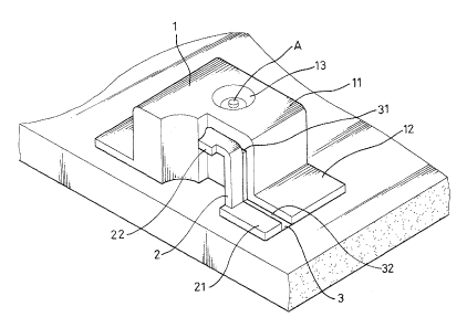
Referring to Fig. 1, basically, an adhesive type LED lead frame according to
CA 02428401 2003-05-09
3
the present invention includes a crystal base 1, a positive pole plate 2 and a
joint 3,
which is between the crystal base 1 and the positive pose plate.
iNherein, the crystal base 1 is a solid base as a negative pole and it is made
of
conductive material. The crystal base 1 at the center thereof has a seat part
11 with
an elevation higher than rest part thereof and at two opposite sides thereof
has a tow
adhesive part 12 respectively with a flat bottom and an elevation lower than
the seat
part 11. The adhesive part 12 can be adhered to a printed circuit board during
the
crystal base 1 being attached to the circuit board. The base part 11 is
thicker than the
melt part 12 to facilitate heat dissipation and there is a locating recess 13
at the top of
the base part 11 for receiving a solid crystal or a chip A.
The positive pole plate 2 is disposed at a lateral side of the crystal base 1
and
also made of the same material as the crystal base 1. The positive pole 2 has
a
shape with a sense of direction corresponding to the crystal base 1 with a
flat joining
part 21 horizontally disposed for being adhered to the circuit board and a
connecting
part 22 extending upward and making a bend near the locating recess 13. The
positive pole plate 2 is used as a positive pole white in use.
In fact, the crystal base 1 can be integrally formed with the positive pole
plate 2
by way of pressing, wax free casting, etching, powder metallurgy, die casting,
extrusion forming, forging, stamping and etc. Hence, in order to facilitate
fabrication,
the base joint 3 is formed with a thinner thickness between the crystal base 1
and the
base part 11. That is, the base joint 31 is between the connecting part 22 and
the
base part 11 and a fiat joint 32 is between the adhesive part 12 and the flat
joining
part 21 so that an integral piece can be constituted before being worked.
While the preceding LED lead frame of the present invention is in use, the
base joint 31 is removed by way of such as being cut off after the solid
crystal or chip
A being placed in the locating recess and connected to a wire B and then it is
CA 02428401 2003-05-09
packaged such that the base part 11 at the top thereof is joined to the top of
the
connecting part 22 to form a state of firmness as shown in Fig. 3. Next, the
flat joint
32 is removed to result in the positive plate 2 is separate from the crystal
base 1
completely. In this way, it is not possible to occur the phenomenon of short
circuit. Fig.
4 shows a perspective view after package.
As the foregoing, the lead frame of the present invention can be adhered to
the
circuit board to constitute a state of close circuit so that a trouble
resulting from
conventional pin insertion can be avoided.
In case of two or more solid crystals or chips, with reference to Fig. 2, the
crystal base 1 at another lateral sides provides a second positive pole plate
4 at a
side and a third positive pole plate 5 at another side so as fio be opposite
to each
other with the locating recess 13 as a center thereof. ~y the same token, the
sec~nd
and the third positive pole plates 4, 5 can be integrally formed with the
crystal base 1
and have a thinner lower joint respectively. Then, the second and the third
positive
pole plates 4, 5 are removed sequentially before and after packaging. In this
way, it is
formed a configuration of three positive poles being disposed at both sides of
the
negative pole crystal base 1 so as to be used in case of two or more solid
crystals or
chips.
With reference to Fig. 5, the third embodiment of the present invention is
illustrated. The crystal base 1 at another lateral sides provides a second
positive pole
plate 4 at a side and a third positive pole plate 5 at another side so as to
be opposite
to each other with the locating recess 13 as a center thereof. By the same
token, the
second and the third positive pole plates 4, 5 can be integrally formed with
the crystal
base 1 and have a thinner lower joint respectively. Then, the second and the
third
positive pole plates 4, 5 are removed sequentially before and after packaging.
In this
way, it is formed a configuration of three positive poles being disposed at
both sides
of the negative pole crystal base 1 so as to be used in case of two or more
solid
CA 02428401 2003-05-09
crystals or chips. Wherein, the first positive pole plate 2 is disposed at a
lateral side of
the crystal base 1 with the same material as the crystal base 1 and has a
shape with
a sense of direction corresponding to the crystal base 1. Thus, the first
positive pole
plate 2 has a horizontal flat joining part 21 adhered to the circuit board and
a
5 connecting part 22 extending upward and near the locating reces:~ 13. The
second
positive pole plate 4 and the third positive pole plate 5 are disposed at
another lateral
side of the crystal base 1 and is made with the same material as the crystal
base 1
with the shape and the sense thereof corresponding to the crystal base 1 so
that a flat
joining part 41, 51 is provided (not shown respectively for being adhered to
the circuit
IO board with a connecting part 42, 52 extending upward near the locating
recess 13
respectively. Wherein, the first, second and third positive pole plates 2, 4,
5 hive the
same thickness as the crystal base 1 and are used as a positive pole
respectively in
practice.
In case of the preceding embodiment of the present inveni:ion is in use, the
base joint 3 is removed by way of such as being cut off after the solid
crystal or chip A
being placed in the locating recess and connected to a wire B and then it is
packaged
such that the positive plate 2 is separate from the crystal base 1 completely.
In this
way, it is not possible to occur the phenomenon of short circuit. Fig. 5 shows
a
perspective view after package.
It is appreciated that the adhesive type LE~ lead frame according to the
present invention can be made with performing to prevent inconvenience from
stamping bends done with conventional art and avoid defective products so as
to
provide an advantage of consistent quality and dimensions. Fuirthermore, it
can
enhance effects of conductivity and heat dissipation due to the crystal base 1
being
solid so as to increase the stability of light emitting device.
While the invention has been described with reference to a preferred
embodiment thereof, it is to be understood that modifications or variations
may be
CA 02428401 2003-05-09
easily made without departing from the spirit of this invention, which is
defined by the
appended claims.