Note: Descriptions are shown in the official language in which they were submitted.
CA 02428412 2007-10-29
TELECOMMUNICATIONS JACK SUBASSEMBLY
Field of the Invention
The present invention relates generally to cross-connect assemblies
and, in particular, to jack assemblies for digital cross-connect systems.
Background of the Invention
A digital cross-connect system (DSX) provides a location for
interconnecting two digital transmission paths. The apparatus for a DSX is
located
in one or more frames, or bays, usually in a telephone central office. The DSX
apparatus also provides jack access to the transmission path.
DSX 'are well known in the art e.a
jacks ( b., see U.S. Patent
Nos. 6,116,961; 5,393,249; 5,145,416; and 4,840,568 that are assigned to ADC
Teleconvnunications, Inc.). A typical jack includes a plurality of bores
(i.e., poits)
sized for receiving tip-and-ring plugs. Spring contacts are provided adjacent
to the
bores for contacting the tip-and-ring plugs. In use, DSX jacks are typically
electrically connected to digital transmission lines, and are also
electrically
connected to a plurality of wire termination members used to cross-connect the
jacks. By inserting plugs within the bores of the jacks, signals transmitted
through
the jacks can be interrupted or monitored.
Sumniaryo of the Invention
One aspect of the present invention relates to a telecommunications
apparatus comprising:
A. a dielectric insert body;
B. a plurality of jacks fastened to the insert body, each of the jacks
including:
i) a jack body defining first, second and third ports positioned such
that the second port is generally between the first and third ports;
ii) a first set of spring contacts positioned adjacent the first port;
iii) a second set of spring contacts positioned adjacent the second
port;
iv) a third set of spring contacts positioned adjacent the third port;
C. each of the jacks being secured to the insert body by a single fastener,
the single fasteners being positioned between the second and third ports of
1
CA 02428412 2007-10-29
each of the jacks, each single fastener being electrically connected to its
corresponding jack body, wherein electrically conductive reinforcing members
are positioned between the insert body and retaining portions of the single
fasteners, and wherein the electrically conductive reinforcing members are
electrically connected together such that all of the jack bodies can be
commonly
grounded.
Another aspect of the present invention relates to a telecommunications
apparatus comprising:
A. a dielectric insert body;
B. a plurality of jacks fastened to the insert body, each of the jacks
including:
i) a jack body defining first, second and third ports positioned such
that the second port is generally between the first and third ports;
ii) a first set of spring contacts positioned adjacent the first port;
iii) a second set of spring contacts positioned adjacent the second
port;
iv) a third set of spring contacts positioned adjacent the third port; and
C. each of the jacks being secured to the insert body by at least a first
fastener wherein the first fastener is electrically connected to its
corresponding
jack body, wherein electrically conductive reinforcing members are positioned
between the insert body and retaining portions of the first fasteners, and
wherein
the electrically conductive reinforcing members are electrically connected
together such that all of the jack bodies can be commonly grounded.
A variety of advantages of the invention will be set forth in part in the
description that follows, and in part will be apparent from the description,
or may
be learned by practicing the invention. It is to be understood that both the
foregoing general description and the following detailed description are
exemplary and explanatory only and are not restrictive of the invention as
claimed.
Yet another aspect of the invention concerns a telecommunications
apparatus comprising:
A. a chassis having oppositely positioned first and second sides;
2
CA 02428412 2007-10-29
B. a plurality of signal lamps positioned at-the first side of the chassis;
C. an IN/OUT panel including an array of IN and OUT connection locations
positioned at the second side of the chassis;
D. a cross-connect panel including an array of cross-connect connection
locations positioned at the second side of the chassis;
E. an insert body connected to the first side of the chassis;
F. a plurality of jacks fastened to the insert body, each of the jacks
including:
i) a jack body defining an IN port, an OUT port and a MONITOR port;
ii) a first set of spring contacts positioned adjacent the IN port;
iii) a second set of spring contacts positioned adjacent OUT port;
iv) a third set of spring contacts positioned adjacent the MONITOR
port; and
v) a lamp switch for activating a corresponding one of the signal
lamps when a plug is inserted in the MONITOR port;
G. the first sets of spring contacts being electrically connected to the cross-
connect panel and the IN/OUT panel;
H. the second sets of spring contacts being electrically connected to the
cross-connect panel and the IN/OUT panel; and
1. the third sets of spring contacts being electrically connected to
corresponding ones of the second sets of spring contacts such that signals
transmitted through the second sets of spring contacts can be monitored by
inserting plugs in the MONITOR ports; and
J. each of the jacks being secured to the insert body by a single fastener,
the single fasteners being positioned between the second and third ports of
each of the jacks.
Still another aspect of the invention concerns a telecommunications
apparatus comprising:
A. a dielectric insert body including a front side and a back side, the
dielectric insert body having a jack mount portion and a lamp mount portion,
the
jack mount portion and the lamp mount portion being unitarily formed as a
single
piece part; the jack mount portion comprising a plurality of columns, each
2a
CA 02428412 2007-10-29
column including a first opening, a second opening, and a third opening; the
lamp mount portion comprising a plurality of lamp openings;
B. a plurality of jacks individually fastened to the back side of the insert
body
at the jack mount portion, each of the jacks including:
i) a jack body defining first, second and third ports positioned such
that the second port is generally between the first and third ports, each of
the
first, second and third ports defined by first, second and third sleeves, the
first,
second and third sleeves being sized for receipt by the first, second and
third
openings of the insert body respectively;
ii) a first set of spring contacts positioned adjacent the first port;
iii) a second set of spring contacts positioned adjacent the second
port; iv) a third set of spring contacts positioned adjacent the third port;
and
C. a plurality of signal lamps mounted at the lamp openings of the lamp
mount portion of the insert body;
D. a plurality of fasteners, each fastener accessible from the front side of
the
dielectric insert body to removeably fasten the jacks to the back side of the
dielectric insert body.
Yet another aspect of the invention concerns a telecommunications
apparatus comprising:
A. a dielectric insert body including a front side and a back side, the
dielectric insert body having a jack mount portion and an lamp mount portion,
the lamp mount portion being connected directly to the jack mount portion such
that no gaps are provided between the jack mount portion and the lamp mount
portion; the jack mount portion comprising a plurality of columns of openings,
each column including a first opening, a second opening, and a third opening;
the lamp mount portion comprising a plurality of lamp openings;
B. a plurality of jacks, each jack fastened to the back side of the insert
body
at the jack mount portion, each of the jacks including:
i) a jack body defining first, second and third ports positioned such
that:
a) the second port is generally between the first and third ports;
2b
CA 02428412 2007-10-29
b) the first port is defined by a first sleeve of the jack body, the
first sleeve being sized for receipt by one of the first openings;
c) the second port is defined by a second sleeve of the jack
body, the second sleeve being sized for receipt by one of the second openings;
d) the third port is defined by a third sleeve of the jack body,
the third sleeve being sized for receipt by one of the third openings;
ii) a first set of spring contacts positioned adjacent the first port;
iii) a second set of spring contacts positioned adjacent the second
port;
iv) a third set of spring contacts positioned adjacent the third port; and
C. a plurality of signal lamps mounted at the lamp openings of the lamp
mount portion of the insert body;
D. a plurality of fasteners, each fastener accessible from the front side of
the
dielectric insert body to removeably fasten the jacks to the back side of the
dielectric insert body.
Brief Description of the Drawings
The accompanying drawings, which are incorporated in and
constitute a part of the description, illustrate several aspects of the
invention and
together with the description, serve to explain the principles of the
invention. A
brief description of the drawings is as follows:
Fig. I is a front, perspective view of a loaded DSX chassis
constructed in accordance with the principles of the present invention;
Fig. 2 is a rear, perspective view of the chassis of Fig. 1;
Fig. 3 is a rear, elevational view of the chassis of Fig. 1;
Fig. 4 is a side, elevational view of the chassis of Fig. 1;
Fig. 5 is a cross-sectional view of the chassis of Fig. 1 taken along a
vertical cross-sectional cutting plane;
Fig. 6 is a front, perspective view of a jack insert subassembly
constructed in accordance with the principles of the present invention;
Fig. 7 is a rear, perspective view of the jack insert subassembly of
Fig. 6;
Fig. S is a front, elevational view of the jaclc insert subassembly of
Fig. 6;
2c
CA 02428412 2007-10-29
Fig. 9 is a top, plan view of the jack insert subassembly of Fig. 6;
Fig. 10 is a cross-sectional view taken along section line 10-10 of
Fig. 9;
Fig. 11 is an exemplary wiring schematic for one of the jacks of the
chassis of Fig. 1;
2d
CA 02428412 2003-05-09
WO 02/39549 PCT/US01/46092
Fig. 12 illustrates a portion of the jack insert subassembly with the
LED spring contacts exploded for clarity;
Fig. 13 illustrates a jack constructed in accordance with the principles
of the present invention;
Fig. 14 shows the jack of Fig. 13 with a plug inserted in the monitor
port and a lamp switch of the jack oriented in a closed position;
Fig. 15 illustrates a second jack constructed in accordance with the
principles of the present invention;
Fig. 16 illustrates a third jack constructed in accordance with the
principles of the present invention;
Fig. 17 illustrates a fourth jack constructed in accordance with the
principles of the present invention;
Fig. 18 illustrates a fifth jack constructed in accordance with the
principles of the present invention;
Fig. 19 illustrates a sixth jack constructed in accordance with the
principles of the present invention; and
Fig. 20 illustrates a seventh jack constructed in accordance with the
principles of the present invention.
Detailed Description
Reference will now be made in detail to exemplary aspects of the
present invention which are illustrated in the accompanying drawings. Wherever
possible, the same reference numbers will be used throughout the drawings to
refer
to the same or like parts.
I. DSX CHASSIS
Figs. 1-5 illustrate a DSX chassis 20 (i.e., a box, module or housing)
constructed in accordance with the principles of the present invention. The
chassis'
20 includes a front side 22 (shown in Fig. 1) positioned opposite from a rear
side 24
(shown in Fig. 2). Ports for receiving tip-and-ring plugs 26 are provided at
the front
side 22 of the chassis. The ports are arranged in upper and lower arrays 27
and 29.
Each of the arrays 27 and 29 includes a horizontal row of IN ports 28, a
horizontal
row of OUT ports 30 and a horizontal row of MONITOR ports 32. Additionally, a
horizontal row of LED ports 34 is provided above each of the upper and lower
arrays 27 and 29. The LED ports 34 are configured for receiving light
sources/lamps such as light emitting diodes 36(shown in Fig. 6). The chassis
20 also
includes front flanges 37 for mounting the chassis in a bay of a
telecommunications
rack or frame.
3
CA 02428412 2003-05-09
WO 02/39549 PCT/US01/46092
As shown in Fig. 2, the chassis 20 further includes a X-CONN panel
38 (i.e., a cross-connect panel) and an IN/OUT pane140. The X-CONN pane138
and the IN/OUT pane140 are located at the rear side 24 of the chassis 20 and
are
staggered or offset relative to one another. The X-CONN pane138 includes
multiple
arrays of cross-connect locations. By way of non-limiting example, the cross-
coimect locations are provided by wire termination members (i.e., wire wrap
pins
39) that project outwardly from the rear side 24 of the chassis 20. However,
it will
be appreciated that other types of contacts or connectors can also provide the
connection locations.
As best shown in Fig. 3, the connection locations provided at the X-
CONN pane138 include tracer lamp (TL) connection locations, tip normal-out (TN-
OUT) connection locations, ring normal-out (RN-OUT) connection locations, tip
normal-in (TN-IN) connection locations and ring normal-in (RN-IN) connection
locations. As used herein, the term "panel" will be understood to mean any
type of
structure at which connection locations can be provided.
Still referring to Fig. 3, the IN/OUT pane140 includes a plurality of
arrays of IN/OUT connection locations. While any type of known electrical
connector can provide the connection locations, the connection locations are
shown
as being provided by wire termination members in the form of wire wrap pins
39.
The arrays of IN/OUT connection locations provided at the IN/OUT pane140
include tip-out (T-OUT) connection locations, ring-out (R-OUT) connection
locations, tip-in (T-IN) connection locations and ring-in (R-IN) connections
locations. Also provided at the rear side 24 of the chassis 20 is a
power/voltage
connection location 42, chassis ground connection location 44, battery ground
connection location 46 and a shield ground connection location 48.
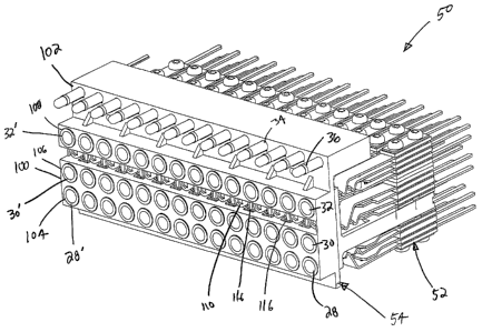
II. JACK INSERT SUBASSEMBLY
Referring back to Fig. 1, each of the upper and lower arrays 27 and
29 of ports is formed by three separate jack insert subassemblies 50 that are
mounted
in the chassis 20. Preferably, the jack insert subassemblies 50 are connected
to the
chassis 20 by conventional techniques such as fasteners. In Fig. 1 the
fasteners are
covered by a rectangular fascia. Figs. 6-10 show one of the jack insert
subassemblies 50 in isolation from the chassis. The depicted jack insert
subassembly 50 includes fourteen separate DSX jacks 52 secured to a common
jack
insert body 54. Preferably, the jack insert body 54 is made of a dielectric
material
such as plastic.
4
CA 02428412 2003-05-09
WO 02/39549 PCT/US01/46092
i. Representative Jack Configuration
Fig. 10 is a cross-sectional view through one of the jacks 52 of the
jack insert subassembly 50 depicted in Figs. 6-9. Jack 52 includes a frame 56
preferably made of a conductive material (e.g., a metal such as die cast
zinc). The
frame 56 includes a forward face 58 and a rearwardly extending spring mount
60.
The forward face 58 includes a monitor sleeve 32' defining MONITOR port 32, an
out sleeve 30' defining OUT port 30 and an in sleeve 28' defiriing IN port 28.
A
stack of contact springs is secured to the spring mount 60 of the frame 56 by
two
fasteners 62 (e.g., bolts, pins or screws). As is conventionally known in the
art, the
stacked springs are preferably separated by dielectric spacers 64. Dielectric
spacers
66 and 68 are also provided for isolating the fasteners 62 from the springs.
The
fasteners 62 are preferably in electrical contact with the frame 56 (e.g., at
the region
the fasteners 62 pass through the spring mount 60). A grounding spring 70 is
electrically connected to the fasteners 62 to provide a connection location
for
grounding the frame 56 to the shield ground 48 of the chassis 20.
The stack of contact springs includes a first set of springs positioned
adjacent the IN port 28, a second set of springs positioned adjacent the OUT
port 30,
and a third set of springs positioned adjacent the MONITOR port 32. The first
set of
springs includes an in ring spring 72, a corresponding in ring normal spring
74, an in
tip spring 76 and a corresponding in tip normal spring 78. The second set of
spring
contacts include an out ring spring 80, a corresponding out ring normal spring
82, an
out tip spring 84 and a corresponding out tip normal spring 86. The third set
of
spring contacts includes a monitor ring spring 88 and a monitor tip spring 90.
Each
of the springs has rear wire wrap portions 91 for allowing the springs to be
connected to corresponding connection locations at the cross-connect pane138
or the
IN/OUT panel 40 of the chassis 20.
A lamp switch 92 is positioned between the second and third sets of
spring contacts (i.e., the lamp switch 92 is positioned between spring
contacts 80-84
corresponding to the OUT port 30 and spring contacts 88, 90 corresponding to
the
MONITOR port 32). When the chassis 20 is wired, the lamp switch 92 is
preferably
electrically connected to LED 36 such that when the lamp switch 92 is closed,
LED
36 is activated (i.e., illuminated or caused to flash).
The lamp switch 92 is preferably caused to close when a plug is
inserted within the MONITOR port 32. In the embodiment of Fig. 10, the lamp
switch 92 includes first and second contact springs 94 and 96. The second
contact
spring 96 is preferably bent or otlierwise provided with a bias (See Fig. 14
where the
bend of the spring 96 is visible) that inherently urges the second contact
spring 96
toward the closed position. As shown in Figs. 10 and 13, the second contact
spring
5
CA 02428412 2003-05-09
WO 02/39549 PCT/US01/46092
96 is held in an open position by a dielectric spacer 98 mounted on the
monitor tip
spring 90. Preferably, the monitor tip spring 90 balances/counteracts the bias
of the
second contact spring 96 and prevents the second contact spring 96 from
contacting
the first contact spring 94. However, when a plug is inserted in the monitor
port 32
as shown in Fig. 14, the monitor tip spring 90 is forced upwardly by the plug
thereby
displacing the dielectric spacer 98 from the second contact spring 96. With
the
dielectric spacer 98 displaced, the natural bias of the second contact spring
96 causes
the second contact spring 96 to move into contact with the first contact
spring 94
thereby closing the lamp switch 92 and illuminating the LED 36.
It is noted that in a typical prior art jack such as the one disclosed in
U.S. Patent No. 5,145,416, the lamp switch is provided above the monitor tip
and
ring springs. In contrast, the lamp switch 92 of the present invention is
positioned
below the monitor springs 88 and 90 at a location between the monitor springs
88
and 90 and the springs 80-86 corresponding to the OUT port 30. By placing the
lamp switch 92 at such a position, it is possible to reduce the height or
profile of the
jack 52 as compared to the prior art. This reduction in height assists in
increasing
the circuit density of the chassis 20.
ii. Jack Insert Body Configuration
Referring back to Fig. 6, the jack insert body 54 of the jack insert
subassembly 50 includes a jack mount portion 100 and an LED mount portion 102.
The jack mount portion 100 and the LED mount portion 102 are preferably formed
as a single, unitary piece. For example, the portions 100 and 102 can be
molded as a
one-piece plastic part. In the preferred embodiment, no fasteners for
connecting the
insert body 54 to the chassis are provided in the region between the two
portions 100
and 102. Further, in the preferred embodiment, no gap or spacing is provided
between the two portions 100 and 102.
The jack mount portion 100 includes an array of openings for
receiving the monitor sleeves 32', the out sleeves 30' and the in sleeves 28'
of the
jacks 52. For example, the jack mount portion 100 includes a first horizontal
row of
openings 104 for receiving the in sleeves 28', a second horizontal row of
openings
106 for receiving the out sleeve 30', and a third horizontal row of openings
108 for
receiving the monitor sleeves 32'. The LED mount portion 102 defines a
horizontal
row of the LED ports 34 that are sized for receiving the light emitting diodes
36. By
making the jack mount portion 100 and the LED mount portion 102 a single
unitary
piece, it has been determined that the overall height of the structure can be
reduced
thereby helping to maximize the circuit density of the chassis 20.
6
CA 02428412 2003-05-09
WO 02/39549 PCT/US01/46092
Referring to Figs. 6, 8 and 10, each of the jacks 52 is secured to the
jack insert body 54 by a single fastener 110 (e.g., a screw or bolt).
Preferably, the
fastener 110 is made of an electrically conductive material (e.g., a metal
such as
zinc-plated steel). As shown in Fig. 10, the fastener 110 extends through an
opening
112 defined by the jack insert 54 and connects with the frame 56 of the jack
52 (e.g.,
the fastener is shown threaded into the frame 56). It is preferred for the
fastener 110
to be located between the MONITOR port 32 and the OUT port 30. By using a
single fastener positioned at a central location of the jack 52, it is
possible to reduce
the overall height of the jack insert subassembly 50 as coinpared to prior art
subassemblies that have fasteners adjacent the top and bottom of the jack.
Referring to Fig. 10, a reinforcing member 114 is preferably
positioned between the head of the fastener 110 and the jack insert 54. The
reinforcing member 114 essentially functions as a washer-type structure. If
the
reinforcing member 114 is made of an electrically conductive material,
conductive
linking members 116 (best shown in Figs. 6 and 8) can be used to electrically
couple
all of the reinforcing members 114 of the jack insert subassembly 50. By
electrically linking the reinforcing members 114 together, all of the jack
frames 56
mounted on the jack insert body 54 can be commonly grounded to the chassis
shield
ground through only one of the ground springs 70 of the 14 jacks. Further, the
linking members 116 can facilitate assembly of the jack insert subassembly 50
by
allowing all of the reinforcing members 114 to be simultaneously mounted in
the
jack insert body 54.
iii. LED Mounting Configuration
Referring again to Fig. 10, the LED 36 includes a main body 118 on
which a lens 120 is mounted. A dielectric spacer/extension 122 projects
outwardly
from the back end of the main body 118. Electrical leads 124 also project
outwardly
from the rear end of the main body 118. The leads 124 are separated, and
electrically isolated by the spacer 122. Preferably, the spacer 122 provides
spacing
between the leads 124 that is substantially less than a diameter of the main
body 118
of the LED 36. This reduction in spacing between the leads 124 assists in
minimizing the height of the LED mount portion 102 of the jack insert 54.
Referring to Figs. 7, 10 and 12, the LED mount portion 102 of the
jack insert body 54 defines upper spring mounting slots 126 and lower spring
mounting slots 128. Upper conductors 130 are mounted in the upper slots 126,
and
electrically connect with the upper leads 124 of the LEDs 36. Lower conductors
132
are mounted in the lower slots 128 and electrically contact the lower leads
124 of the
LEDs 36. The conductors 130 and 132 include barbs or tabs 134 that embed in
the
7
CA 02428412 2003-05-09
WO 02/39549 PCT/US01/46092
material forming the LED mount portion 102 of the jack insert body 54 to
prevent
the conductors 130 and 132 from dislodging from the slots 126 and 128.
Preferably,
the conductors 130 and 132 are mounted in the slots 126 and 128 in a manner in
accordance with the teaching of U.S. Patent No. 4,870,753, that is hereby
incorporated by reference.
The upper conductors 130 include base portions 136 that are firmly
secured in the upper slots 126, and spring portions 138 having base ends
connected
to the base portions 136. From their base- ends, the spring portions 138
extend in a
forward direction within the LED mount portion 102. Free ends of the spring
portions 138 are biased into contact with the upper leads 124 of the LEDs 36.
The lower conductors 132 include base portions 139 that are firmly
secured in the lower slots 128. The lower conductors 132 also include spring
portions 140 that extend from the base portions 139 in a rearward direction
and are
biased into contact with the lower leads 124 of the LEDs 36. Thus, the spring
portions 138 of the upper conductors 130 extend in an opposite direction as
compared to the spring portions 140 of the lower conductors 132.
The lower conductors 132 also include connection members 142
sized to be received in a quick-connect style electric connector. The
connection
members 142 include offset portions 143 that project perpendicularly outwardly
from the base portions 139, and contact portions 145 that project
perpendicularly
from the offset portions 143. As shown in the Fig 12, the contact portions 145
are
generally parallel with respect to the base portions 139. Preferably, each of
the
connection members 142 is positioned in alignment with a corresponding one of
the
spring portions 140. Referring to Fig. 7, when the lower conductors 132 are
mounted in the insert body 54, the connection members 142 are positioned
within
vertical gaps 144 defined by the LED mount portion 102 of the jack insert body
54.
Preferably, the lower conductors 132 are electrically tied together to
form a strip as shown in Fig. 12. In use, the lower conductors 132 are
preferably
connected to a common power/voltage source. The raised connection members 142
facilitate connecting the lower springs 132 to the power source by providing
connection locations for connecting a wire to the electrically linked
conductors 132.
For example, by inserting a quick connect over one of the various connection
members 142, the entire strip of lower conductors 132 can be quickly wired to
a
power source. Additionally, the raised connection members 142 allow the lower
conductors 132 of the various jack insert subassemblies 50 to be easily
electrically
connected together (e.g., by s single jumper between adjacent jack
subassemblies
50). To facilitate inserting a quick connector over the connection members
142,
portions of the LED mount portion 102 can be cut-away to provide additional
8
CA 02428412 2003-05-09
WO 02/39549 PCT/US01/46092
clearance. For exainple, portions of the LED mount portion 102 can be cut away
adjacent the second connecting members 142 corresponding to the second and
thirteenth jacks of the subassembly.
Unlike the lower conductors 132, the upper conductors 130 are
preferably not electrically interconnected with one another. In use, each of
the
springs 130 includes a wire wrap member 152 for allowing each upper conductor
130 to be electrically connected to its corresponding lamp switch 92. When the
lamp switch 92 is closed, the corresponding upper conductor 130 is
electrically
connected to ground thereby causing power to be supplied to the LED 36 such
that
the LED 36 is lighted.
III. EXEMPLARY WIRING CONFIGURATION FOR CHASSIS
Fig. 11 shows an exemplary wiring schematic for one of the jacks 52
within the chassis 20. As shown in Fig. 11, the in spring contacts 72 and 76
are
wired to the T-IN and R-IN connection locations at the IN/OUT pane140, and the
in
normal spring contact 74 and 78 are wired to the TN-IN and RN-IN connection
locations at the X-CONN panel 38. Similarly, the out spring contacts 80 and 84
are
wired to the T-OUT and R-OUT connection locations of the IN/OUT panel, and the
out normal springs 82 and 86 are wired to the TN-OUT and RN-OUT connection
locations of the X-CONN panel 38. Further, the monitor ring spring 88 is
electrically connected to the out ring spring 80, and the monitor tip spring
90 is
electrically connected to the out tip spring 84. Moreover, the first contact
spring 94
of the lamp switch 92 is electrically connected to the battery ground and the
second
contact spring 96 of the lamp switch 92 is electrically connected to a tracer
lamp
connection location TL at the cross-connect panel 38, and to the LED 36 which
is
connected to the power source. Furthermore, the grounding spring 70 is
electrically
connected to the shield ground 48 of the chassis 20.
In use, cross-connection of a signal from another jack enters the
chassis 20 as an IN signal through connection locations TN-IN and RN-IN of the
X-
CONN pane138. With no plugs inserted within the IN port 28, the IN signal is
output from the chassis 20 at the T-IN and R-IN connection locations of the
IN/OUT
pane140.
By inserting a plug within the IN port 28, the IN signal from a cross-
connected jack can be interrupted and a signal from the inserted plug can be
outputted at points T-IN, R-IN of the IN/OUT pane140. Similarly, by inserting
a
plug within the OUT port 30, an OUT signal from contact points T-OUT and R-
OUT of the IN/OUT panel 40 may be outputted to the tip-and-ring contacts of
the
plug inserted within the OUT port 30.
9
CA 02428412 2003-05-09
WO 02/39549 PCT/US01/46092
Frequently, it is desirable to be able to monitor OUT signals arriving
through the T-OUT and R-OUT contacts of the IN/OUT pane140 without
interrupting the OUT signals. To accomplish this, a plug is inserted into the
MONITOR port 32. On this occurrence, the plug taps into the OUT signals being
transmitted through out springs 80-86. Additionally, when the plug is inserted
into
the MONITOR port 32, the second contact spring 96 of the lamp switch 92 is
allowed to flex upwardly to close the lamp switch 92. With the lamp switch 92
closed, power is provided to the LED 36. It will be appreciated that the LED
36 can
include an integrated circuit chip for controlling flashing of the LED 36 as
is
conventionally known in the art. In addition to activating the LED 36, the
closure of
the lamp switch 92 also grounds the tracer lamp line TL causing illumination
of the
LED of a jack to which the present jack is cross-connected.
IV. ALTERNATE JACK CONFIGURATIONS
Fig. 15 illustrates a second jack 152 having the same configuration as
the jack 52 except that dielectric spacer 98 secured to monitor tip spring 90
has been
arranged to pass through an opening 103 defined by first contact spring 94 of
lamp
switch 92. Similar to the jack 52, the lamp switch 92 is normally closed. It
will be
understood that the phrase "normally closed" means that the switch will move
to a
closed position unless an additional structure (e.g., spacer 98) is used to
push or hold
the switch open. When no plug is inserted within MONITOR port 32, spacer 98
prevents the second contact spring 96 from engaging the first contact spring
94. By
contrast, when a plug is inserted within the MONITOR port 32, monitor tip
spring
90 is displaced upwardly such that dielectric spacer 98 also is moved
upwardly.
With the dielectric spacer 98 displaced upwardly, the self-bias of the second
contact
spring 96 brings the second contact spring 96 into contact with the first
contact
spring 94 thereby closing the lamp switch 92.
Fig. 16 illustrates a third jack 252 constructed in accordance with the
principles of the present invention. The jack 252 has the same construction as
the
jack 52, except that dielectric spacer 98 has been mounted on second contact
spring
96 as compared to monitor tip spring 90.
Fig. 17 illustrates a fourth jack 352 constructed in accordance with
the principles of the prevent invention. The jack 352 has the same structure
as the
jack 52 except that dielectric spacer 98 has been shortened and an end portion
97 of
second contact spring 96 of lamp switch 92 has been modified to traverse the
distance between second contact spring 96 and spacer 98. For example, the end
portion 97 is shown including an upwardly extending portion 99 that extends
upwardly past the upper spring 94 of the lamp switch 92, and a platform 101
for
CA 02428412 2003-05-09
WO 02/39549 PCT/US01/46092
supporting the spacer 98. Similar to the previous embodiments, second contact
spring 96 is normally biased toward the closed position.
Fig. 18 illustrates a fifth jack 452 constructed in accordance with the
principles of the present invention. The jack 452 has the same construction as
the
jack 52 except that lamp switch 92 is a normally open switch (i.e., the switch
remains open unless an additional structure is used to force the switch
closed).
Instead, in this embodiment, the monitor tip spring 90 positively moves the
second
contact spring 96 through the use of a link 99 providing a connection between
the
monitor tip spring 90 and the second contact spring 96. When no plug is
inserted in
the MONITOR port 30, the lamp switch 92 is open as shown in Fig. 18. By
contrast, when a plug is inserted in MONITOR port 32, the monitor tip spring
90 is
forced upwardly by the plug causing the link 99 to pull the second contact
spring 96
into contact with the first contact spring 94. In this manner, the lamp switch
92 is
positively closed when a plug is inserted in the MONITOR port 32.
Fig. 19 is a sixth jack 552 constructed in accordance with the
principles of the present invention. The jack 552 has a similar construction
to the
jack 52 except the lamp switch 92 is normally open. Further, the jack 552
includes a
dielectric ramp 105 that projects forwardly from the first contact spring 94
to a
location directly below the contact region of the monitor tip spring 90. When
no
plug is inserted in the MONITOR port 32, the lamp switch 92 is open. By
contrast,
when a plug is inserted in the MONITOR port 32, the plug engages the rainp
member 105 and forces the ramp member 105 downwardly causing the first contact
spring 94 to be positively forced downwardly into contact with contact spring
96.
Fig. 20 illustrates a seventh jack 652 constructed in accordance with
the principles of the present invention. The jack 652 has a similar
configuration as
the jack 52 except that the lamp switch 92 is a norinally open switch. Similar
to the
embodiment of Fig. 19, the jack 652 includes a dielectric ramp 107 connected
to the
first contact spring 94 of the lamp switch 92. The ramp 107 has an angled
surface
positioned directly beneath the contact region of the monitor tip spring 90.
When no
plug is inserted in the MONITOR port 32, the lamp switch 92 is open as shown
in
Fig. 20. By contrast, when a plug is inserted within the MONITOR port 32, the
plug
engages the inclined ramp surface of the ramp 107 causing the first contact
spring 94
to be forced downwardly into contact with the second contact spring 96.
Having described preferred aspects and embodiments of the present
invention, modifications and equivalents of the disclosed concepts may readily
occur
to one skilled in the art. However, it is intended that such modifications and
equivalents be included within the scope of the claims which are appended
hereto.
11