Note: Descriptions are shown in the official language in which they were submitted.
CA 02429184 2007-06-22
WO 02/41451 PCT/US01/41908
1
RADIO FREQUENCY ISOLATION CARD
Field of Invention
This invention relates to antennas for communicating electromagnetic signals
and, more particularly, to improving sensitivity of a dual polarized antenna
by
increasing the isolation characteristic of the antenna.
Background of the Invention
Many types of antennas are in wide use today throughout the communications
industry. The antenna has become an especially critical component for an
effective
wireless communication system due to recent technology advancements in areas
such
as Personal Communications Services (PCS) and cellular mobile radiotelephone
(CMR) service. One antenna type that has advantageous features for use in the
cellular telecommunications industry today is the dual polarized antenna which
uses a
dipole radiator having two radiating sub-elements that are polarity specific
to transmit
and receive signals at two different polarizations. This type antenna is
becoming more
prevalent in the wireless communications industry due to the polarization
diversity
properties that are inherent in the antenna that are used to increase the
antenna's
capacity and to mitigate the deleterious effects of fading and cancellation
that often
result from today's complex propagation environments.
Dual polarized antennas are usually designed in the form of an array antenna
and have a distribution network associated with each of the two sub-elements
of the
dipole. A dual polarized antenna is characterized by having two antenna
connection
tenninals or ports for communicating signals to the antenna that are to be
tran.smitted,
and for outputting signals from the antenna that have been received. Thus the
connection ports serve as both input ports and as output ports at any time, or
CA 02429184 2003-05-14
WO 02/41451 PCT/US01/44908
2
concurrently, depending on the antenna's transmit or receive mode of
operation.
An undesirable leakage signal can appear at one of these ports as a result of
a
sigiial present at the opposite port and part of that signal being
electrically coupled,
undesirably so, to the opposing port. A leakage signal can also be produced by
self-
induced coupling when a signal propagates through a power divider and feed
network.
The measuring of leakage signals is illustrated in the conventional art of
Figure 1. A main transmission signal al can be inputted at port 35. This
transmission
signal al is propagated by the antenna elements 11 coupled to port 35 when
these
antenna elements 11 are operating in a transmit mode. An undesirable leakage
signal
bl can be measured at port 35 as a result of the transmission signal al
exciting
portions of the feed network such as distribution network 15.
In another example, the undesirable leakage signal b1 can be measured at port
35 when a transmission signal a2 is inputted at port 40. The transmission
signal a2
can excite portions of the feed network such as distribution network 17 which
in turn,
can excite antenna elements 11, 12 or distribution network 15 or both. It is
noted that
other leakage signals (not shown) may be measured at port 40 which are caused
by
transmission signal a2 itself or signals inputted at port 35.
A dual polarized antenna's performance in terms of it transmitting the
inputted signal with low antenna loss of the signal, or of it receiving a
signal and have
low antenna loss at the antenna's output received signal, can be measured in
large part
by the signals' electrical isolation between the antenna's two connection
ports, i.e.,
the port-to-port isolation at the connectors or the minimizing of the leakage
signal bl.
Dual polarized antennas can also have radiation isolations defined in the far-
field of
the antenna which differ from port-to-port isolations defined at the antenna
connectors. The focus of this invention is not on far-field isolation, but
rather with
port-to-port isolations at connector terminals of a dual polarized antenna.
While a dual polarized antenna can be formed using a single radiating
element, the more common structure is an antenna having an array of dual
polarized
radiating elements 10. In practice, both the transmit and receive functions
often occur
simultaneously and the transmit and received signals may also be at the same
frequency. So there can be a significant amount of electrical wave activity
taking
CA 02429184 2003-05-14
WO 02/41451 PCT/US01/44908
3
place at the antenna connectors, or ports, sometimes also referred to as
signal
suanming points.
The significant amount of electrical wave activity during simultaneous
transmission and reception of RF signals can be explained as follows. Poor
receive
sensitivity, and poor radiated output, often results due to degraded internal
antenna
loss when part of one of the signals at one input port (port one) leaks or is
otherwise
coupled as a leakage signal to the other port (port two). Such leakage or
undesired
coupling of a signal from one port to the other adversely combines with the
signal at
the other port to diminish the strength of both signals and hence reduce the
effectiveness of the antenna. When port-to-port isolation is minimal, i.e.,
leakage is
maximum, the antenna system will perform poorly in the receive mode in that
the
reception of incoming signals will be limited only to the strongest incoming
signals
and lack the sensitivity to pick up faint signals due to the presence of
leakage signals
interfering with the weaker desired signals. In the transmit mode, the antenna
performs poorly due to leakage signals detracting from the strength of the
radiated
signals.
Dual polarized antenna system performance is often dictated by the isolation
characteristic of the system and the minimizing or elimination of leakage
signals.
Conventional Isolation Techniques
One known technique for minimizing this leakage signal problem is by
incorporating proper impedance matching within the distribution networks of
the two
respective signals. Impedance mismatch can cause leakage signals to occur and
degrade the port-to-port isolation if (1) a cross-coupling mechanism is
present within
the distribution network or in the radiating elements, or if (2) reflecting
features are
present beyond the radiating elements. Impedance matching minimizes the amount
of
impedance mismatch that a signal experiences when passing through a
distribution
network, thereby increasing the port-to-port isolation.
In general, when impedance mismatches are present, part of a signal is
reflected back and not passed through the area of impedance mismatch. In a
dual
polarized antenna system, the reflected signal can result in a leakage signal
at the
CA 02429184 2003-05-14
WO 02/41451 PCT/US01/44908
4
opposite port or the same port and it can cause a significant degradation in
the overall
isolation characteristic and performance of the antenna system. While
impedance
matching helps to increase port-to-port isolation, it falls short of achieving
the high
degree of isolation that is now required in the wireless communications
industry.
Another technique for increasing the isolation characteristic is to space the
individual radiating elements of the array sufficiently apart. However, the
physical
area and dimensional constraints placed on the antenna designs of today for
use in
cellular base station towers generally render the physical separation
technique
impractical in all but a few instances.
Another technique for improving an antenna's isolation characteristic is to
place a physical wall between each of the radiating elements. Still another is
to
modify the ground plane 30 of the antenna system so that the ground plane 30
associated with each port is separated by either a physical space or a non-
conductive
obstruction that serves to alleviate possible leakage between the two signals
otherwise
caused by coupling due to the two ports sharing a common ground plane 30.
These
techniques can help in increments, but do not solve the magnitude of the
signal
leakage problem.
Still another conventional technique for improving the isolation
characteristic
of an antenna is to use a feedback element to provide a feedback signal to
pairs of
radiators in the antenna array. The feedback element can be in the form of a
conductive strip placed on top of a foam bar positioned between radiators.
While the
conductors, according to this technique, can increase the isolation
characteristic, the
foam bars that support the conductive strips have mechanical properties that
are not
conducive to the operating environment of the antenna. For example, the foam
bars
are typically made of non-conducting, polyethylene foam or plastic. Such
materials
are usually bulky and are difficult to accurately position between antenna
elements.
Additionally, these support blocks have coefficients of thermal expansion that
are typically not conducive to extreme temperature fluctuations in the outside
environment in which the antenna functions, and they readily expand and
contract
depending on temperature and humidity. In addition to the problems with
thermal
expansion, the support blocks are also not conducive for rapid and precise
CA 02429184 2003-05-14
WO 02/41451 PCT/US01/44908
manufacturing. Furthermore, these types of support blocks do not provide for
accurate
placement of the conductive strips or feedback elements on the distribution
network
board.
Another problem with this conventional type feedback element is that the
5 element is typically "floating" above its respective ground plane. That is,
it is not
connected to the ground plane or "grounded". Such an ungrounded feedback
system is
susceptible to electrostatic charging. The electrostatic charging of these
type
conductive elements may attract lightning or currents that are formed from
lightning.
Consequently, there is a need in the art for a method and system that
facilitates
the design of a dual polarized antenna system with a high degree of isolation
between
two respective antenna connection ports that more thoroughly cancels out any
port-to-
port leakage signals and at the same time, is conducive to high speed
manufacturing
and a high degree of accurate repeatability. There is also a need in the art
for an
antenna isolation method and system that can withstand extreme operating
environments as a cellular base station antenna is subjected to, and one that
is also
designed to eliminate any potential problems that are a result from lightning
or fizrther
leakage from electric charge build-up.
Summary of the Present Invention
The present invention is useful for improving the performance of an antenna
by increasing the port-to-port isolation characteristic of the antenna as
measured at the
port connectors. In general, the present invention achieves this improvement
in
sensitivity by using a feedback system comprising one or more feedback
elements for
generating a feedback signal in response to a transmitted signal output by
each
radiator of the dual polarized antenna. This feedback signal is received by
each
radiator, also described as a radiating element, and combined with any leakage
signal
present at the output port of the antenna. Because the feedback signal and the
leakage
signal are set to the same frequency and are approximately 180 degrees out of
phase,
this signal summing operation serves to cancel both signals at the output
port, thereby
improving the port-to-port isolation characteristic of the antenna.
Each feedback element can comprise a photo-etched metal strip supported by
CA 02429184 2003-05-14
WO 02/41451 PCT/US01/44908
6
a dielectric card made from printed circuit board material. Such feedback
elements
can provide a high degree of repeatability and reliability in that the
manufacturing of
such feedback elements can be precisely controlled. For example, the size,
shape, and
location of the feedbaclc elements on the dielectric supports can be
manufactured by
using photo etching and milling processes. Such feedback elements are
conducive for
high volume production environments while maintaining high quality standards.
The
manufactnring processes for such feedback elements provide the advantage of
small
tolerances.
Another important feature of the present invention is the high degree of
control over the material properties of the feedback element support
structure. Each
feedback element support structure is typically an insulative material that
has
electrical and mechanical properties that are conducive to extreme operating
environments of antenna arrays. For example, such feedback element support
structures can be selected to provide appropriate dielectric constants
(relative
permeability), lost tangent (conductivity), and coefficient of thermal
expansion in
order to optimize the isolation between respective antenna elements in an
antenna
array.
The characteristics of the feedback signal, including amplitude and phase, can
be adjusted by varying the position of the feedback element relative to the
radiating
element thereby affecting the amount of coupling therebetween and, hence, the
amount of port-to-port isolation. The feedback signal can be further adjusted
by
placing additional feedback elements into the dual polarized antenna system
until a
specific amount of feedback coupling is produced so to enable the cancellation
of any
leakage signals passing from port 1 to port 2.
For yet another aspect of the present invention, the feedback elements can
comprise etched metal strips disposed upon a planar dielectric support and
fiirther
comprising grounding elements connecting the etched metal strips to the
network
ground plane of an antenna array. In one exemplary embodiment, the ground
element
can comprise a meander line that connects the respective etched metal strip to
the
ground plan of a beam forming the network. In another exemplary embodiment,
the
grounding element can comprise the rectilinear etched metal strip of an
appropriate
CA 02429184 2003-05-14
WO 02/41451 PCT/US01/44908
7
width.
It is further noted that the feedback elements may be positioned in a variety
of
configurations with equal success, such as non-uniform feedback element
spacing
(non-symmetrical patterns), and tilted feedback elements (introducing a
rotational
angle). It is fiuther noted that the conductive element may be in varying
forms or
shapes, for example, the elements may be in the form of strips as well as
circular
patches.
In one exemplary embodiment, the feedback elements can be combined with
dual polarized antenna radiators. In such an exemplary embodiment, the
feedback
elements may improve the isolation characteristic of signals between two
different
polarizations.
In an alternate exemplary embodiment, the feedback elements can be
combined with multiple band radiating antenna elements. In this way, signals
between different operating frequencies can be isolated from one another.
In view of the foregoing, it will be readily appreciated that the present
invention provides for the design and tuning method of a dual polarized
antenna
system or a multiple band antenna system having a high port-to-port isolation
cllaracteristic thereby overcoming the sensitivity problems associated with
prior
antenna designs. Other features and advantages of the present invention will
become
apparent upon reading the following specification, when taken in conjunction
with the
drawings and the appended claims.
Brief Description of Drawings
Figure 1 is a block diagram illustrating some of the core components of a
conventional dual polarized array antenna, showing the radiator sub-elements,
the
feed networks, the two connector ports of the antenna system, and signals
depicted at
both ports.
Figure 2 is an illustration showing an elevational view of the construction of
an exemplary embodiment of the present invention, showing the isolation card
with
its feedback elements.
Figure 3 is an illustration showing a longitudinal side view of the exemplary
CA 02429184 2003-05-14
WO 02/41451 PCT/US01/44908
8
embodiment shown in Figure 2 and the relative positions of the isolation cards
with
the radiating elements of the antenna.
Figure 4 is an end side view of the antenna shown in Figures 2 a.nd 3
depicting
the relative dimension of the feedback element and a dipole radiator.
Figure 5 is an illustration showing an isometric view of the exemplary
embodiment shown in Figures 2 and 3.
Figure 6 is a side view of the antenna systein shown in Figures 2 and 3.
Figure 7 is a bottom view of a part of the antenna system according to one
exemplary embodiment that shows a locating aperture for the support structure
of a
feedback element.
Figure 8 is an isometric view of an enlarged part of the antenna system
according to another exemplary embodiment that shows multiple slots for the
location
of the support structures of the feedback elements.
Figure 9 is another isometric view of an antenna illustrating the positioning
of
a feedback element provided with the first exemplary grounding elenzent.
Figure 10 is another isometric view of an antenna illustrating the positioning
of feedback element provided with the second exemplary type of grounding
element.
Figure 11 is an illustration showing an elevational view of the construction
of
alternate exemplary embodiment of the present invention where isolation cards
are
positioned between multiple band radiators.
Figure 12 is another isometric view illustrating multiple feedback elements
provided on an isolation card.
Figure 13 is a functional block diagram illustrating various orientations of
isolation cards relative to radiating antenna elements.
Detailed Description of Exemplary Embodiments
The isolation card of the present invention can solve the aforementioned
problems of leakage signals in, especially, a dual polarized antenna and is
usefitl for
enliancing antenna performance for wireless communication applications, such
as
base station cellular telephone service.
Turning now to the drawings, in which like reference numerals refer to like
CA 02429184 2003-05-14
WO 02/41451 PCT/US01/44908
9
elements, Figure 1 is a diagram that illustrates the basic components of a
conventional
dual polarized antenna 5. Input/output ports 35 and 40 are the connection
ports, or
antenna terminals, for inputting and/or receiving signals 20. Each port is
connected to
its respective distribution network 15, 17 that communicates the signal to one
of the
two differently polarized sub-elements 11 and 12 in a dual polarized radiator
of the
antenna. In one exemplary embodiment, the dual polarized radiator comprises a
crossed dipole 10. Signals of ports 35 and 40 communicate with a four-element
array
made of dipole radiator elements 10, although it is understood that there can
be any
number of radiators making up the antenna array.
Basic to antenna operation is the principal of reciprocity. An antenna
operates
with reciprocity in that the antenna can be used to either transmit or receive
signals, to
transmit and receive signals at the same time, and to even transmit and
receive signals
concurrently at the same frequency. It is understood, therefore, that the
invention
described is applicable to an antenna operating in either a transmit or
receive mode or,
as is more normally the case at a cellular antenna base station, operating in
both
modes simultaneously. The invention operates basically the same way regardless
of
whether the antenna is transmitting or receiving dual polarized signals at its
radiating
elements 10.
For simplicity in the description that follows, the antenna system is
described
generally as operating in a transmit mode. The isolation card 45 of the
invention, like
the dual polarized antenna of one exemplary embodiment, operates basically the
same,
way regardless of whether the antenna is transmitting or receiving dual
polarized
signals at its radiating elements 10. The depiction of Figure 1 thus also
shows the
overall antenna as transmitting or receiving signals 20.
Also for the purpose of illustrating the present invention, the preferred
embodiment is described in terms of its application to an antenna having dual
polarized, dipole radiating elements 10, with it understood that use of the
invention is
not limited to this type of antenna.
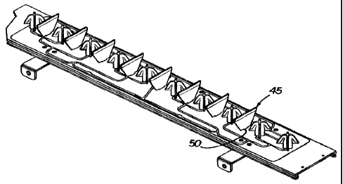
Figure 2 is an illustration showing an elevational view of one exemplary
embodiment depicting the isolation cards 45 of the invention installed in a
dual
polarized antenna 5 formed by ten dipole radiator elements 10 in a single
column
CA 02429184 2003-05-14
WO 02/41451 PCT/US01/44908
array. The isolation cards 45 are positioned along a vertical plane of the
antenna as
viewed normal to the longitudinal plane of the antenna. The antenna 5 shown is
for
communicating electromagnetic signals with high frequency spectrums associated
with conventional wireless communication systems.
5 The antenna 5, which can transmit and receive electromagnetic signals, can
comprise radiating elements 10, a ground plane 30, and distribution feed
networks 15,
17 associated with each of the respective sub-elements 11, 12 of the radiating
elements 10. The antenna 5 further comprises a printed circuit board (PCB) 26,
two
terminal antenna connection ports 35 and 40 for inputting and receiving dual
10 polarized signals, and the isolation card feedback system comprising
isolation cards
45 spaced between the radiating elements 10.
The feedback system comprising the isolation cards 45 provides for the
electrical coupling of feedback signals to and from the radiating elements 10
in a
manner to cancel out undesired leakage signals, thereby facilitating
improvement of
the antenna's isolation characteristic.
Each crossed dipole radiator 10 in the array comprises two dipole sub-
elements 11 and 12 (Figs. 1 and 5) that provide for the dual polarization
characteristic
in both the transmit and receive modes. Dipole sub-element 11 of each crossed
dipole
radiator 10 is linked together to all otlier like dipole sub-elements 11, and
correspondingly, dipole sub-element 12 of each crossed dipole is linked
together to all
other like dipole sub-elements 12, and connect to the two respective
distribution
networks 15, 17 to correspond with the dual polarized signal (either transmit
or
receive) present at antenna ports 35, 40, respectively (Figs. 1 and 2).
The dual polarized radiating elements 10 are each aligned in a slant (45
degrees) configuration relative to the array (longitudinal axis), so to
achieve the best
balance in the element pattern symmetry in the presence of the mutual coupling
between the elements. Distribution networks 15, 17 each include a beam forming
networlc (BFN) 20, 22 respectively that incorporates a power divider network
25, 27
respectively for facilitating array excitation (Fig. 2).
In combination with the radiating elements 10, a conductive surface operative
as a radio-electric ground plane 30 (Fig. 2) supports the generation of
substantially
CA 02429184 2003-05-14
WO 02/41451 PCT/US01/44908
11
rotationally symmetric patterns over a wide field of view for the antenna. The
ground
plane 30 is positioned underneath and adjacent to the distribution networks
15, 17 and
over which the radiating elements 10 are coupled relative thereto. Fig. 3 also
shows
the isolation cards 45 are operatively positioned within the dual polarized
antenna
system relative to the radiating elements 10 so to achieve the desired amount
of
coupling between the radiating elements 10 and the feedback elements 55.
Referring now to Fig. 5, each feedback element 55 can comprise a photo-
etched metal strip supported by a planar dielectric support 65 made from
printed
circuit board material. The feedback element 55 on each isolation card 45 can
comprise a single conductive strip. Alternatively, it can comprise spaced-
apart, photo-
etched conductive strips, with many different spacing configurations, with
equal
success in achieving the improved port-to-port isolation characteristic for
the antenna.
Such feedback elements 55 can provide a high degree of repeatability and
reliability in that the manufacturing of such feedback elements 55 can be
precisely
controlled. For example, the size, shape and location of the feedback elements
55 on
the dielectric support can be manufactured by using photo etching and milling
processes. Such feedback elements 55 are conducive for high volume production
environments while maintaining high quality standards. The manufacturing
processes
for such feedback elements 55 provide the advantage of small tolerances.
Figures 3 and 4 also show that the isolation cards 45 are distributed in a
consistent fashion with one card 45 positioned between every two radiating
elements
10, aligned along a perpendicular to the center line 13 (Fig. 2) of the
antenna 5, and
positioned relatively midway between any two adjacent radiators 10. That is,
the
distance X (Fig. 3) between a respective radiator 10 and an isolation card 45
is
maximized such that each isolation card 45 is as far away from an adjacent
pair of
radiating elements 10 as possible. With such an arrangement, the possibility
of the
isolation cards 45 distorting the impedance of the radiating elements 10 is
substantially eliminated.
Because of the midway positioning of the isolation cards 45, it follows that
the
relative spacing S 1 between respective cards 45 is substantially equal to the
spacing
S2 between respective radiating elements 10 when the radiating elements 10 are
CA 02429184 2003-05-14
WO 02/41451 PCT/US01/44908
12
positioned in a uniform manner. In this exemplary embodiment, the spacing S2
between the radiating elements 10 is approximately three-quarters (3/4) of the
operating wavelength. Accordingly, the corresponding spacing S1 of the
isolation
cards 45 is also approximately three quarters (3/4) of the operating
wavelength.
However, other spacings can be used based on the coupling desired and
variations
from the three quarter wavelength used in the preferred embodiment are within
the
scope of the invention. In other words, uniform and non-uniform spacing
between
respective isolation cards 45 themselves or spacing between isolation cards 45
and
antenna elements 10 can be employed without departing from the scope and
spirit of
the present invention.
One important feature of the present invention is the high degree of control
over the material properties of the feedback element support structure. Each
isolation
card support structure is typically an insulative material that has electrical
and
mechanical properties that are amenable to extreme operating environments of
antenna arrays. For example, such support structure can be selected to provide
appropriate dielectric constants (relative permeability), lost tangent
(conductivity) and
coefficient of thermal expansion in order to optimize the isolation between
respective
antenna elements in an antenna array.
Referring back to Fig. 5, the isolation card 45 is made of a dielectric
material
that forms a planar dielectric support 65 with a narrow bottom end 70 for
connecting
to the printed circuit board (PCB). The dielectric material of the isolation
card 45 can
comprise one of many low-loss dielectric materials used in radio circuitry. In
the
preferred embodiment, it is made from a material known in the art as MC3D (a
mediunl frequency dielectric laminate manufactured by Gill Technologies). MC3D
is
a relatively low-loss material and is fairly inexpensive. The dielectric
constant of
MC3D is approximately 3.86. However, the present invention is not limited to
this
dielectric constant and this particular dielectric material. Other dielectric
constants
can fall generally within the range of 2.0 to 6Ø The dielectric support used
has a
dissipation factor of 0.019. However, other low-loss type dielectric materials
with
different dissipation factors are not beyond the scope of the present
invention.
CA 02429184 2003-05-14
WO 02/41451 PCT/US01/44908
13
The isolation card 45 used in this exemplary embodiment has a thickness of 31
mils. However, other thicknesses can also be used. The narrow portion 70 is
typically
a function of the size of the aperture 50 in the printed circuit board. At its
opposite
end, the isolation card 45 has a wide portion 80 that is typically a function
of the
length L (Fig. 5) of the feedback element 55. However other shapes, different
from
that shown in Figure 5, can be selected depending upon ease of manufacturing
as well
as efficient and economic use of the dielectric material that forms the
isolation card
45. For example, to minimize the amount of dielectric material used, the
support
could be formed as a "T" shape. The shape should be chosen to maximize
mechanical
rigidity of the isolation card 45 while minimizing unnecessary excess
dielectric
material that does not contribute to the card's mechanical rigidity or
strength.
The feedback element 55 on the isolation card 45 is positioned near the top
thereof and, in the preferred embodiment comprises a conductive strip running
parallel to the PCB 26 as illustrated in Fig. 5. The conductive strip can be
electro-
deposited or rolled copper. In one exemplary embodiment, the conductive strip
is
photo-etched (by use of photolithography) on the dielectric material. This
method is
very conducive to high speed, high volume, and precision controlled
manufacturing
capabilities. The feedback elements 55 may also be attached to the dielectric
material
of the isolation card 45 by soldering them to metal pads etched onto the
isolation card
45, or by using an adhesive.
Referring now to Figure 6, Length L of the conductive strip is three-fifths
(3/5) of the operating wavelength. However, the present invention is not
limited to
this resonant length. The length of the conductive strip can be approximately
0.4 to
0.6 wavelength in this embodiment. As a general rule of thumb, the length of
the
conductive strip is typically an unequal number of half wavelengths.
The height H of the conductive strip is illustrated in Figure 6 relative to
the
antenna's ground plane 30, and is approximately equal to the height of the
radiating
element 10. That is, the conductive strip can be aligned in a parallel manner
with its
adjacent radiating elements 10. However, this exemplary height parameter can
be
changed to optimize the degree of coupling depending upon the particular
application
at hand.
CA 02429184 2003-05-14
WO 02/41451 PCT/US01/44908
14
The width W of the conductive strip (Fig. 5) can be adjusted or tuned to
various widths. This width W is typically chosen to provide sufficient
operating
iinpedance bandwidth that is similar to that of the radiating elements 10. The
resonant
length of the conductive strip can vary as the width of the conductive strip
is adjusted.
In other words, the conductive strip feedback element 55 can be made of
various
widths and lengths to provide the required resonance effect depending upon the
frequencies involved and the specific application at hand. It is further noted
that the
width directly affects the amount of coupling that can be achieved by each
feedback
element 55 and, thus, the width (like the length) may vary from one
application to
another depending on the amount of required coupling.
Connection of the isolation card 45 to the PCB is usually completed with the
use of an aperature in the PCB 26 as shown in Figure 5. Aperture 50 receives
the
bottom portion 70 of the isolation card 45 to allow the card to be precisely
positioned
between respective pairs of radiating elements 10.
Referring to Figure 7, a connector 110 is positioned in the aperture and
penetrates through the PCB and contains openings 112 for making electrical
connections to the ground plane 30, if desired. Apertures 50 in combination
with the
connectors 110 provide for rapid and consistent placement of the isolation
cards 45
between the radiating elements 10. Additional mounting options are possible
using the
apertures to increase the mechanical rigidity of the isolation cards 45 such
as, for
example, by adding "kick stands" to the support structure.
Further details of the connector forming the aperture 50 are illustrated in
Figure 7 showing a bottom view of the aperture connector. Connector mechanisms
100, such as solder pads, are placed on one side of the connector to give
additional
mechanical stability to the isolation card 45. In this exemplary embodiment,
the
connector mechanisms 100 do not provide any electric purpose. On the opposing
side
of the connector there are additional connecting mechanisms 110 that comprise
the
electrical connections via plated thru-holes.
Figure 8 illustrates an alternate embodiment showing additional apertures 50
with connecting mechanisms 110 that can be incorporated into the PCB 26 for
alternative antenna configurations utilizing the isolation cards 45 with the
same type
CA 02429184 2003-05-14
WO 02/41451 PCT/US01/44908
of feed network. The additional slots 50 allow for precise positioning of the
isolation
cards 45. The apertures 50 can be formed by lrnown milling processes.
Turning now to the functioning of the isolation card 45, the isolation card 45
is
set at a position relative to adjacent dipoles to generate feedback signals
via the
5 resonating feedback elements 55 on each isolation card 45 to cancel leakage
signals
present at antenna connection ports 35, 40. A feedback signal can be generated
by a
feedback element 55 resonating in response to the first polarized signal at
the dipole
sub-element 11. This feedback signal can then be coupled back into the second
polarized signal at sub-element 12 on the same dipole radiator. The feedback
signal
10 can cancel the leakage signal because the feedback signal is identical in
frequency and
is 180 degrees out-of-phase from the source signal.
Similarly, another feedback signal can be generated by a feedback element 55
resonating in response to a second polarized signal produced at the dipole sub-
element
12. This feedback signal can be coupled back into the first polarized signal
at sub-
15 element 11.
To obtain a complete cancellation of a leakage signal, the feedback signal
usually must have an amplitude equal to the amplitude of the respective
leakage
signal. The exact positioning of the feedback elements 55 can be empirically
determined and is often a function of the feedback elements 55 receiving
electromagnetic signals of a certain amplitude or strength from those
transmitted (or
received) by the radiating elements 10.
Einpirical measurements can be conducted to determine the proper number of
isolation cards 45 and the proper orientation of each relative to the
radiators 10, to
obtain a feedback signal having the appropriate amplitude so as to achieve the
complete cancellation of a leakage signal at either of the antenna's two
connection
ports. By "tuning" the antenna with the appropriate amount of coupling, a
feedback
signal having the correct amplitude will be produced which, in turn, will
result in the
desired amount of isolation being achieved within the antenna system.
This tuning is a function of the feedback element 55 design on the isolation
card 45 and the height and spacing of the card relative to adjacent radiators.
Ultimately, the actual spacing and configuration of the feedback elements 55
will
CA 02429184 2003-05-14
WO 02/41451 PCT/US01/44908
16
depend upon the particular application at hand to generate a strength or
amplitude of
feedback signal needed to cancel out any leakage signals at ports 35, 40.
Each feedback signal contributes to the generation of an aggregate feedback
signal having the desired amplitude and phase characteristics. Thus, when the
two
feedback signals sum with the leakage signal at either antenna connector ports
35, 40,
the leakage signals are canceled by the 180 degree phase difference of the
feedback
signals.
An alternate embodiment of the isolation card 45' is illustrated in Figure 9,
where a different feedback element 55' includes a grounding element 90A. The
grounding element 90A can be formed as a high impedance meandering line that
gives a direct current (DC) connection between feedback element 55' and the
ground
plane 30.
This grounding element 90A is basically a wire with very high inductance, and
in this embodiment it has a width of approximately 10 mils. The width is
typically
chosen so that it is not difficult to etch on the dielectric support 65. The
thickness of
the grounding element 90A as well as the conductive strip 60 is approximately
1.5
mils. However, other thickness of this material may be used and still remain
within
the scope of the invention.
The function of grounding element 90A is to drain any charges that may build
up on the conductive strip 60 during operation of the antenna system. This
insures that
the conductive strip is at the same voltage potential as the ground plane 30
in order to
reduce the possibility of the conductive strip being charged and attracting
lightning.
Therefore, the grounding element 90A is designed to only transmit, short to
ground,
DC currents and not RF currents.
As a third embodiment, Figure 10 illustrates another type feedback element
55"'. This element 55"' comprises a conductive strip grounding element 90B
with a
design that can more readily support induced currents as a result of
unbalanced dipole
balun radiation. This grounding element design gives greater protection
against
lightning, and it also has more of an RF impact than the meandering line type
90A in
Figure 9.
CA 02429184 2003-05-14
WO 02/41451 PCT/US01/44908
17
In each of the embodiments, the feedback element 55 may be disposed on both
sides of the isolation card 45, as depicted by the functional block in Fig. 8.
The
feedback element 55 may be left floating, or grounded to the network ground
plane 30
through plated th.ru-holes as illustrated in Figure 10.
In summary, the isolation card 45 employs materials with well-defined
electrical parameters that remain constant in typical antenna array operating
environments, and allows use of feedback elements 55 that are conducive to
high
speed, high volume, and precision-controlled manufacturing capabilities.
Manufacturing of the isolation card 45, and particularly the feedback element
55 on
the card, are highly repeatable and their designs allow for easy control and
design
flexibility in the shape of the feedback signal path by microstrip or other
conductive
path design created on the dielectric support with a high precision that is
possible
with etching processes.
The feedback elements 55 are typically used on base station, dual-pole slant
+I- 45 degree antennas for wireless communications operating at frequency
ranges of
2.4 Gigahertz (GHz). They typically provide a port-to-port isolation greater
than 30
decibels. It is noted that while the isolation characteristics of the
radiating elements 10
improved by one or two decibels compared to the conventional feedback elements
that employ conductors on Styrofoam blocks, the far field antenna radiation
patterns
were also cleaner or more well-behaved than those produced by feedback
elements
disposed on Styrofoam blocks. It is an added benefit that the feedback
elements 55,
while substantially reducing near field cross coupling to improve the
isolation in a
dual polarized antenna, they also improve the antenna's far field radiation
characteristics.
The location of the isolation card 45 can be precisely controlled by apertures
50 that are disposed in the PCB 26. The dielectric support 65 for each
feedback
element 45 may or may not include "kick stands" for additional mechanical
support.
Additional apertures 50 can be incorporated into the printed circuit board
material 26
for alternative antenna configurations using the same beam forming network.
Referring now to Figure 11, this figure illustrates another exemplary
operating
enviromnent for the inventive isolation card 45. In this exemplary embodiment,
CA 02429184 2003-05-14
WO 02/41451 PCT/US01/44908
18
isolation cards 45 are positioned between multiple band radiators 10' of
antenna
system 1100. Further, in this exemplary embodiment, multiple isolation cards
45 can
be stacked upon one another in order to provide enhanced leakage signal
reduction
and increased isolation between ports of the antenna system. In this
particular and
exemplary embodiment, one set of isolation cards 45 is oriented in a parallel
manner
with a central axis 13 wliile another set of isolation cards 45 is
perpendicularly
oriented with the central axis 13.
The radiators 10' can comprise patch antenna elements that can operate in
multiple frequency bands. However, as noted above the present invention is not
limited to one type of antenna element. Therefore, other types of radiating
elements
are not beyond the scope of the present invention. Other radiating antenna
elements
include, but are not limited to, monopole, microstrip, slot, and other like
radiators.
With the isolation cards 45, RF signals between multiple frequency bands can
be
isolated from one another similar to the dual polarization antenna system
illustrated in
Figure 2.
Referring now to Figure 12, this figure illustrates another isometric view of
multiple feedback elements 55 provided on an isolation card 45. Specifically,
an
isolation card 55 can further comprise multiple feedback elements 55 that can
be
placed proximate to one another to provide additional feedback signals.
Referring to Figure 13, this Figure illlustrates a top view or an elevational
view of the antenna elements 10 and isolation cards 45. The arrow labeled "A"
indicates that each isolation card 45 can be rotated to a desired angle that
maximizes
the cancellation of any leakage signals that may be sent to a port. A group of
antenna
elements 10 could have RF Isolation cards 45 oriented at various angles to
maximize
cancellation of any leakage signals that are generated between antenna
elements of an
element array.
Although the embodiments of the present invention have been described with
particularity to several different feedback mechanisms in conjunction with
dual
polarized radiator antennas and multiple band radiator antennas, the present
invention
can be equally applied to other types of antennas.
CA 02429184 2003-05-14
WO 02/41451 PCT/US01/44908
19
While the invention has been described in its exemplary forms, it should be
understood that the present disclosure has been made only by way of example
and that
numerous changes in the details of construction and the combination and
arrangement
of parts may be resorted to without departing from the spirit and scope of the
invention. Accordingly, the scope of the present invention is defined by the
appended
claims rather than the foregoing description.