Note: Descriptions are shown in the official language in which they were submitted.
CA 02429778 2003-05-23
Optical Module
B ACKGROUND OF THE INVENTION
1. Field of the Invention
This invention relates to an optical link module, by which an optical signal
is
transmitted and/or received.
2. Related Prior Art
:1n optical link module has an optical transmitting sub-assembly (TOSA)
that converts an electrical signal to an optical signal, and an optical
receiving
sub-assembly (ROSA) that converts the optical signal to the electrical signal.
1 o These TOSA and ROSA are enclosed within a housing so as connected to a
wiring
substrate. Such optical link module has been disclosed in the USP 6,074,228.
The TOSA, the ROS A and the wiring substrate are arranged and fixed
within the housing. In the link module with a pluggable function, the accurate
position of the wiring substrate is required to connect the board with
external
terminals. When the wiring substrate is rigidly fixed within the housing to
secure
the positional accuracy, a residual stress due to a difference of the thermal
expansion coefficient of assemblies is accumulated in the portion where the
TOSA
and the ROSA are fixed to the wiring substrate, which causes a deformation and
a
deterioration of a reliability of the module.
2 o SUMMARY OF THE INVENTION
The present invention is to solve the problem that the residual stress is
accumulated in the connection portion of the TOSA/R,OSA to the wiring
substrate,
thereby enhancing the operational stability.
CA 02429778 2003-05-23
An optical module according to the present invention comprises an
optical sub-assembly, a wiring substrate, a housing having a front space, a
rear
space and a stopper provided between the front space and the rear space, and a
holder for holding the wiring substrate. The wiring substrate mounts
electrical
parts thereon and is electrically connected to the optical sub-assembly. The
front
apace of the housing encloses the optical sub-assembly and the rear space
thereof
encloses the wiring substrate. The front space, the stopper and the rear space
are
arranged along a hypothetical axis in this order. The holder has a resilient
portion
f«r pressing the substrate toward the front space so as to butt the wiring
substrate
against the stopper.
In the present optical module, the wiring substrate is held by holder and
pressed against the stopper of the housing by the resilient portion of the
holder.
Therefore, the position of the wiring substrate along the hypothetical axis is
accurately decided without firmly fining the substrate to the housing. This
configuration enables to compensate the difference of the thermal expansion
between the wiring substrate and the housing, which prevents the accumulation
of the residual stress and enhances the reliability of the module.
The wiring substrate of the present invention preferably has a first pox-tion
with a first width, a second portion with a second width greater than the
first
width, and a taper provided between the first portion and the second portion.
The
holder preferably comprises a base with an opening through which the first
portion of the wiring substrate is inserted, and the resilient portion
disposed so as
t.o sandwich the opening. These configuration of the wiring substrate and the
CA 02429778 2003-05-23
3
holder enables to hold the wiring substrate by inserting the first portion
thereof
through the opening and to position the wiring substrate without firmly fixing
to
the housing by pressing it toward the front space along the hypothetical axis.
In the present invention, the holder preferably comprises latches and the
housing preferably comprises a pair of side wall having a latch for hooking
the
latch of the holder. By hooking mechanism between latches, the wiring
substrate
can be fried to the housing.
In the optical module according to the present invention, the side wall
preferuhly has a groove extending along the hypothetical axis for guiding the
wiring substrate. This groove makes it simple to enclose the wiring substrate
into
the housing by guiding the substrate along the groove. Further, the groove
preferably has at least a pair of inner wall and an elastic piece for pressing
the
wiring substrate against one of the inner wall of the groove. This
configuration
may position the wiring substrate along a direction normal to the hypothetical
axis without firmly fixing to the housing.
In the optical module according to the present invention, the optical sub-
assembly preferably comprises a first portion having a first diameter, a
second
portion having a second diameter smaller than the first diameter, and a step
for
connecting the first portion to the second portion. Further, the housing
preferably
2 o has an optical receptacle next to the front space along the hypothetical
axis and a
partition with a hole piercing from the front space to the optical receptacle.
The
optical sub-assembly is preferably arranged so that the second portion thereof
is
inserted in the hole and the step butts against the partition. This
configuration
CA 02429778 2003-05-23
4
enables t;o position the sub-assembly along the hypothetical axis.
In the optical module according to the present invention, the optical sub-
assembly preferably has a plurality of lead terminals for electrically
connecting
the ub-assembly to the wiring substrate. The lead terminals preferably
sandwich
the wiring substrate and have a resilient characteristic. This configuration
enhances not only the productivity of the module but also the reliability of
the
module.
In the optical module according to the present invention, the optical sub-
a~aemlaly may be a transmitting optical sub-assembly (TOSA) or a receiving
optical sub-assembly (ROSA). Further, the optical module of the present
invention
can contain the TOSA and the ROSA.
BRIEF DESCRIPTION OF THE DRAWINGS
Figure 1 is an exploded view illustrating the optical module of the present
znventzon;
Figure 2 is a bottom perspective view of the optical module;
Figure 3 is an upper perspective view of the optical module;
Figure 4A and figure 4B show a configuration of the holder;
Figure 5 illustrates the position of the respective elements comprising the
optical module; and
2 o Figure 6 illustrates a configuration when the optical module is installed
on
an ext.crn u1 board containing a host connector.
DEVILED DESCRIPTION OF THE EMBODIMENT
The preferred embodiments of the present invention will be described. In the
CA 02429778 2003-05-23
drawings, Elements identical to each other will be referred to with numerals
identical t.o each other without overlapping explanations.
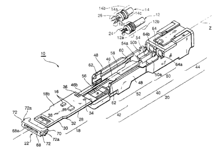
h'igure 1 is a perspective view from the bottom side of an optical link module
1() according to the present embodiment. The link module 10 has a transmitting
optical sub-assembly (TOSA) 12, a receiving optical sub-assembly (ROSA) 14, a
wiring substrate on which a plural electrical parts are mounted, a holder 22
for
securing the wiring substrate, and a housing 20 for enclosing the TOSA, the
ROSA and the wiring substrate therein.
The transmitting optical sub-assembly 12 comprises a first portion 12a with
l0 a tubular shape for enclosing a light-emitting device, such as a laser
diode, and a
second portion 12b with a tubular shape. The second portion 12b contains a
ferrule through which a tip of an optical fiber is inserted and a sleeve for
holding
the ferrule. An outer diameter of the first portion is greater than that of
the
second portion, whereby a step 12c is formed at the boundary between two
portions. Three lead terminals 24 are extended from the first portion. These
lead
terminals correspond to a signal with a normal phase, a signal with a reverse
phase, and a signal of an optical monitor.
'fhe receiving optical sub-assembly 14 comprises a first portion 14a with a
tubular shape for enclosing a light-receiving device, such as a photo diode,
and a
2 0 second portion 14b with a tubular shape. Similarly to the TOSA, the second
portion 14b contains a ferrule through which a tip of an optical fiber is
inserted
and a sleeve for holding the ferrule. An outer diameter of the first portion
14a is
greater than that of the second portion 14b, whereby a step 14c forms the
CA 02429778 2003-05-23
6
boundary between two portions. Five lead terminals 26 are extended from the
first portion of the ROSA. These lead terminals correspond to a signal with a
normal phase, a signal with a reverse phase, a bias supply for the photo
diode, a
power supply and a ground, respectively.
The wiring substrate 18 is a printed-circuit board made of multi-layered
resin material and has a substantially rectangular shape. Portions of both
sides
are cut, thereby forming a first portion 28 with a first width, a second
portion 30
with a second width narrower than the first width, and taper 32 therebetween.
Some electrical parts 16, such as an IC for driving the light-emitting device
in the
to TOSA 12 and another IC for processing signals received by the light-
receiving
device in the ROSA 14, are mounted on the both surfaces of the wiring
substrate.
A region near the front edge of the wiring substrate provides a terminal 34
for the TOSA 12 and plural terminals 36 for the ROSA, similarly, the front
surface
of the wiring substrate provides plural terminals for the TOSA 12 and also for
the
ROSA 14. These terminals provided in the front edge of the front surface are
not
shown in .Fig. 1.
A rear edge of both surfaces of the wiring substrate provides plural terminals
38 for contacting to an electrical connector 92 shown in Fig. 6. These
terminals
correspond ground terminals, power supply terminals, and signal terminals.
The housing 20 comprises a body 40, a connector cover 42 for covering the
electrical connector 92 in Fig. 6, and an optical receptacle 44 for receiving
an
optlc~il connector. The body 40, the connector cover 42 and the receptacle 44
are
arranged along the hypothetical Z-axis.
CA 02429778 2003-05-23
The body 40 has an upper wall 46 and a pair of side walls 48. These walls are
arranged along the Z-direction and forms a space surrounded therewith. The
front
space 5() encloses the TOSA 12 and the ROSA 14 therein, while the rear space
52
sets the wiring substrate 18. The front space 50 comprises of a TOSA mounting
apace 50a and a ROSA mounting space 50b by a partition 54 extending along the
Z-direction. The stopper 54a, which butts against the wiring substrate 28 and
prevents the substrate 28 from shaking, is provided at the end of the
partition.
As shown in Fig. 3, the upper wall 46 of the body 40 comprises a front wall
4fa, a rear wall 46b and a rib 46c connecting the front wall 46a to the real
wall
4fib. Thee front wall 46a configures the front space 50, and the inner surface
thereof supports the TOSA and the ROSA. On the other hand, the rear wall 46b
configures the rear space 52 and connects to the connector cover 42. An
opening is
formed in the center of the rear wall 46b, within which an elastic sheet 56 is
attached and held by the rear edge of the opening.
A yoove 58 for guiding the wiring substrate 18 is formed in the inner surface
of the side wall 48. The front edge of the groove 58 provides an elastic piece
60,
which is capable to bend up and down as the wiring substrate 18 is inserted in
the
groove. Further, a latch 62 is formed in the inner surface close to the rear
edge of
the side wall 48 to hold the holder 22. The respective grooves have at least a
pair
of inner surface, one of which is pressed against the wiring substrate.
'fhe optical receptacle 44 is separated from the front space 50 by the
partition wall 64 orthogonal to the Z-direction. The receptacle has a pair of
openings 66a, 66b for mating an optical connector 94 provided in the tip of
the
CA 02429778 2003-05-23
8
optical fiber as illustrated in Fig. 6. The pair of openings 66a, 66b
corresponds to
the TOS:A mounting space and the ROSA mounting space, respectively. The
opening E~6a is connected to the TOSA mounting space 50a by a hole 64a
provided
in the partition wall, while the opening 66b is connected to the ROSA mounting
space 50b by a hole 64b.
The holder 22 includes a base portion 68, a resilient portion 70 and a side
portion 72. The base portion has an opening 68a through which the second
portion
of the wiring substrate 18 is inserted. The resilient portion 70 builds up
from the
base portion and surrounds the opening. The side portion builds up from the
l0 resilient portion 70 and has a latch 72a in an outer surface thereof. The
holder 22
is hooked to the housing 20 by the latch 72a with the other latch 62 provided
in
the inner surface of the side wall 48. The hooking mechanism of the holder 22
to
the housing 20 is performed by the pair of latch formed in the respective
inner
surface of the side wall and the corresponding latch provided in the holder
22.
The TOSA 12 is placed in the TOSA mounting space 52a as the second
portion thereof is inserted into the hole 64a provided in the partition 64 as
shown
in Fig. 4. 'The position of the TOSA 12 along the z-direction is decided by
the
configuration that the step 12c of the TOSA butts against the partition 64.
Similarly, the ROSA 14 is placed in the ROSA mounting space 52b in the housing
20 as the second portion thereof is inserted into the hole 64b. The position
of the
ftOSA 14 along the z-direction is decided by the configuration that the step
14c of
the ROSA 14 butts against the partition 64.
The wir ing substrate 18 is enclosed in the rear space 52 of the housing 22.
CA 02429778 2003-05-23
9
The subar.rate, which is guided from the side of the connector cover 42 and
toward
the front edge thereof by the pair of the groove 58 in the side wall 48, butts
against
the stopper 54a of the partition 54. The wiring substrate 18 is secured by the
holder 22 as the second portion 30 thereof with relatively narrower width is
inserted into the opening 68a and the taper 32 is pressed against the
resilient
portion 'l0 of the holder 22. The latch 72a provided in the both side of the
holder
22 are hooked with the corresponding latch 62 provided in the inner surface of
the
aide wall 48 of the housing. The wiring substrate 18 is pressed downward by
the
elastic: piece 60, while the front edge thereof butt against the stopper 54a
of the
1 o partition 54, whereby the position of the substrate 18 along the z-
direction is
defined. Moreover, the wiring substrate is pressed downward by the elastic
sheet
5E~ provided in the rear wall 46 and the pair of the elastic piece 60
respectively
provided in the front edge of the groove 58, whereby the substrate 18 is
pressed
against the one of the inner surface of the groove 48, as shown in Fig. 6.
The TOSA 12 is arranged as three lead terminals 24 thereof sandwiches the
wiring substrate 18 from the both surfaces, and the ROSA 14 is arranged as
five
lead terminals 26 thereof sandwiches the substrate 18. These lead terminals
24,
26 are fixed to respective terminals 34, 36 on the wiring substrate 18. The
lead
terminals 24, 26 preferably has a resilient characteristic to contact firmly
to the
2 o tE'T1x11Ilals 34, 36, thereby enhancing the productivity of the module.
Since the wiring substrate 18 is secured under the upper wall 46 with a room
th~neto, as illustrated in Fig. 6, it is able to install electrical parts in
both surfaces
thereof, which realizes the high density assembly. The rear edge of the wiring
CA 02429778 2003-05-23
aubatrate 18 projects from the rear space 52 and extends to the connector
cover
4,~.
This optical link module is installed in the external board 90 where the host
conne<aor 92 is provided. The host connector 92 has a receptacle 92a for
mating
5 with the wiring substrate 18. Within the receptacle 92 of the host
connector, plural
lead tcrrrainals 92b are provided for electrically connecting to the terminals
38 on
the wiring substrate 18. When the link module 10 is installed in the external
board 90, the host connector 92 is enclosed with the connector cover 42 of the
hou sing 20 and the receptacle 92a thereof mates with the rear edge of the
wiring
to substrate 18. This makes electrical contact between the terminals 38 on the
substrate' 18 and the corresponding lead terminals 92b within the receptacle
92a.
When the link module 10 is to be released, the rear edge of the wiring
substrate is
pulled out from the receptacle 92a. Thus, the optical link module 10 according
to
the present embodiment has terminals to be electrically connected to the lead
terminals ~~2b of the host connector in the rear edge portion of the wiring
substrate, thus realizing a hot-pluggable arrangement.
The optical link module 10 according to the present invention, the holder 22
aecurcs the wiring substrate 18 as the second portion 30 thereof with a
relatively
narrow er width is inserted into the opening 68a of the holder 22 that is
arranged
2 o by latching mechanism provided between the holder 22 and the housing 20.
The
tajper 32 of the wiring substrate 18 is pressed against the resilient portion
70 of
the holder. The elastic force of the resilient portion 70 presses forward the
wiring
aubstraite 18, whereby the front edge ofthe board 18 butt against the stopper
54a
CA 02429778 2003-05-23
11
c>f the partition 54. Therefore, the holder 22 accurately places the wiring
substrate
18 within the housing 20 without firmly fixing thereto, which relaxes the
difference of the thermal expansion co-efficient between the board 18 and the
housing 20. In beneral, the thermal expansion co-efficient of the resin
material
that comprises of the housing 20 is about 20 ppm/'~, while that of the wiring
substrate is about 10 ppm/'~. By deforming the resilient portion 70 of the
holder
that presses the taper 32 of the wiring substrate along the z-direction, the
difference of the thermal expansion between the parts are compensated. This
configuration enables to release residual stress accumulated in the coupling
portion of the substrate 18 to the lead terminals 24,26, to maintain the
stable
operation, and to enhance the reliability of the module 10.
The link module 10 of the present embodiment has the groove 58 extending
along the z-direction in the inner surface of both side walls 48. This enables
to
guide the wiring substrate 18 into the housing 20 by sliding the substrate 18
within the groove 58. Further, the module 10 has the elastic piece 60 and the
elastic sheet 56 that press the wiring substrate downward. This enables to
enhance the accuracy of the position of the board 18 in a direction normal to
the
G-dll'ect1011.
The positions of the TOSA 12 and the ROSA of the present embodiment are
defined by the arrangement that the second portions 12b, 14b thereof are
inserted
into tho holes 64a, 64b provided in the partition 64 and the respective steps
12c,
14c alre butt to the partition. Further, by closing the first portions of the
TOSA and
t.hc~ RO;~f1 to the rear edge of the partition 54, the length of the lead
terminals can
CA 02429778 2003-05-23
12
be shorten, which decreases the parasitic inductance inherently provided in
the
lead terminal, thereby enhancing the high frequency performance of the module
1(). In the module of the present embodiment, the TOSA and the ROSA are
contacted to the wiring substrate 18 as the plural lead terminals 24, 26
sandwich
the wiring substrate 18, which enables to enhance the productivity of the
module
l.O.
From the invention thus described, it will be obvious that the invention and
its application may be varied in many ways. For example, the embodiment
dcacrihed above has both the TOSA and the ROSA. However, the present
1 o invention may be applicable for the module having only the TOSA or the
ROSA.