Note: Descriptions are shown in the official language in which they were submitted.
CA 02429785 2003-05-23
BALLAST WITH ADAPTIVE END-OF-LAMP-LIFE PROTECTION
Field of the Invention
The present invention relates to the general subject of circuits for
powering discharge lamps. More particularly, the present invention relates to
a
ballast with adaptive end-of-lamp-life protection.
Background of the Invention
In electronic ballasts with a half-bridge type inverter and a direct-coupled
output, it is common for a direct current (DC) blocking capacitor to be
coupled
in series with the lamp. During normal operation of the lamp, the voltage
across
the DC blocking capacitor (VBLOCK) is equal to approximately one-half of the
DC rail voltage (VDC) that is supplied to the inverter. As the lamp approaches
the end of its normal operating life, VBLOCK will tend to depart from its
normal
value of about VDC/2. Thus, a number of existing end-of-lamp-life protection
circuits monitor VBLOCK as a reliable indicator of imminent lamp failure. A
number of these circuits consider a lamp to be in a failure mode when VBLOCK
departs from its normal value by more than a predetermined threshold amount.
In order to adequately protect the ballast from damage and avoid any
possible overheating of the lamp sockets (the latter being a primary concern
with
small diameter lamps, such as T5 lamps), it is highly desirable that the
predetermined threshold amount be suitably small in relation to the normal
value
Of VBLOCK= As an example, in a ballast with VDC = 450 volts, the normal value
of VBLOCK is about VDC/2 = 225 volts. A typical protection circuit will
consider
the lamp to be in the failure mode if VBLOCK departs from its normal value of
225
volts by as little as 10 volts (i.e., 4%) in either direction; that is, the
lamp is
considered to be in the failure mode if VBLOCK either exceeds 235 volts or
falls
below 215 volts. In existing protection circuits, these minimum (i.e., 215
volts)
and maximum (i.e., 235 volts) values are "designed in"; that is, they are
specified on an a priori basis, regardless of the actual value of VBLOCK
during
normal operation.
CA 02429785 2010-10-14
2
The problem with setting such a tight band of detection (e.g., 4%) on an a
priori
basis is that the tolerances of certain components in the ballast render such
an approach
unreliable at best. First, VBLOCK is generally monitored via a resistive
voltage-divider network
that is coupled in parallel with the DC blocking capacitor. The tolerances of
the voltage-
divider resistors are a first source of possible error. Secondly, the
protection circuit itself
generally includes a digital control circuit or microcontroller in which the
supply voltage
(Vc) can vary by as much as 5%. This introduces another possible source of
detection error.
Additionally, small differences in the dead-time and/or duty cycle at which
the inverter
switches are driven will cause VBLOCK to differ at least somewhat from its
ideal normal value
of VpC/2. Also, VDC itself has an associated tolerance (e.g., typically on the
order of about
2% or so). Finally, each of the aforementioned sources of possible error is
temperature-
dependent to some extent, and may thus be aggravated by the often considerable
changes in
temperature that occur during operation of the ballast.
In order to avoid the detection problems arising from component tolerances,
one
would have to set a band of detection that is considerably less tight than in
the above example.
For instance, the band of detection would have to be increased to 20 volts
(rather than 10
volts). Unfortunately, such "opening up" of the band of detection degrades the
quality of
protection afforded by the protection circuit, and may not even be an option
for ballasts that
operate certain types of lamps.
What is needed, therefore, is a ballast with an end-of-lamp-life protection
circuit that
is capable of providing a tight band of detection and that is relatively
insensitive to component
tolerances and other sources of detection error. Such a ballast would
represent a considerable
advance over the prior art.
Summary of the Invention
According to an aspect of the present invention there is provided a ballast
for
powering at least one gas discharge lamp, comprising: a pair of input
connections adapted to
receive a source of alternating current; first and second output connections
adapted for
connection to the gas discharge lamp; an inverter operably coupled between the
input
connections and the first output connection, the inverter including an
inverter drive circuit for
providing inverter switching at a predetermined operating frequency, the
inverter drive circuit
having a protection input and being operable, in response to application of a
fault signal at the
protection input, to take protective action; a direct current (DC) blocking
capacitor coupled
between the second output connection and circuit ground; a control circuit
having a control
input operably coupled to the DC blocking capacitor, and a control output
coupled to the
CA 02429785 2010-10-14
2a
protection input of the inverter drive circuit, wherein the control circuit is
operable: (i)
following initial application of power to the ballast, to measure the voltage
across the DC
blocking capacitor and to store that voltage as a reference value; and (ii)
following each
subsequent application of power to the ballast: (a) to monitor the voltage
across the DC
blocking capacitor; and (b) in response to the voltage across the DC blocking
capacitor
departing from the reference value by more than a predetermined threshold
amount, to
provide the fault signal at the control output.
CA 02429785 2003-05-23
3
Brief Description of the Drawings
FIG. 1 describes a ballast with an end-of-lamp-life protection circuit, in
accordance with a preferred embodiment of the present invention.
FIG. 2 is a flowchart describing the operation of the control circuit in the
ballast described in FIG. 1, in accordance with a preferred embodiment of the
present invention.
FIG. 3 is a flowchart further describing the operation of the control
circuit in the ballast described in FIG. 1, in accordance with a preferred
embodiment of the present invention.
Detailed Description of the Preferred Embodiments
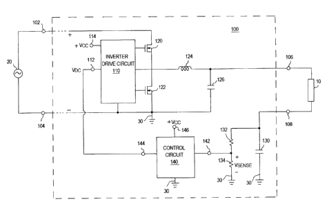
A ballast 100 for powering at least one gas discharge lamp 10 is
described in FIG. 1. Ballast 100 comprises a pair of input connections
102,104,
first and second output connection 106,108, an inverter 110,120,122 with a
series-resonant output circuit 124,126, a direct current (DC) blocking
capacitor
130, and a control circuit 140.
Input connections 102,104 are adapted to receive a source of alternating
current, such as 277 volts (rms) at 60 hertz. Output connections 106,108 are
adapted for connection to gas discharge lamp 10. Direct current (DC) blocking
capacitor 130 is coupled between second output connection 108 and circuit
ground 30.
Inverter 110,120,122 is operably coupled between input connections
102,104 and first output connection 106, and includes an inverter drive
circuit
110 for providing switching of inverter transistors 120,122 at a predetermined
operating frequency. Inverter drive circuit 110 has a supply input 114 for
receiving operating power (+Vcc), and a protection input 112. In response to
application of a fault signal at protection input 112, inverter drive circuit
110
takes protective action (e.g., terminating inverter switching or operating the
inverter at a frequency that is substantially higher than the predetermined
CA 02429785 2003-05-23
4
operating frequency) so as to prevent any damage to the inverter and the lamp
sockets.
Control circuit 140 has a supply input 146 for receiving operating power
(+VCC), a control input 142 that is operably coupled to DC blocking capacitor
130, and a control output 144 that is coupled to the protection input 112 of
inverter drive circuit 110. Control circuit 140 is preferably implemented via
a
suitable programmable microcontroller that is programmed to operate in the
following manner. Following initial application of power to ballast 100,
control
circuit 140 measures the voltage across DC blocking capacitor 130 and stores
that voltage as a reference value. Following each subsequent application of
power to ballast 100, control circuit 140 monitors the voltage across DC
blocking capacitor 130. If the measured voltage across DC blocking capacitor
130 departs from the stored reference value by more than a predetermined
threshold amount (e.g., 10 volts), control circuit 140 provides the fault
signal at
control output 144 (and, therefore, at protection input 112).
Because the actual voltage across DC blocking capacitor 130 is a rather
high value (e.g., 225 volts), it is impractical to monitor or measure that
voltage
directly. Toward this end, ballast 100 further includes a resistive voltage-
divider network comprising a first resistor 132 and a second resistor 134.
First
resistor 132 is coupled between second output connection 108 and control input
142 of control circuit 140. Second resistor 134 is coupled between control
input
142 and circuit ground 30. The voltage across second resistor 134 (e.g., 2.25
volts or so under normal operation) is a scaled down version of the voltage
across DC blocking capacitor 130. During operation, the voltage VSENSE across
second resistor 134 is monitored and measured in lieu of the actual voltage
across DC blocking capacitor 130. Of course, the predetermined threshold
amount is scaled down by the same factor (i.e., 0.1 volts instead of 10
volts). As
an example, if the actual voltage across DC blocking capacitor 130 is normally
225 volts, resistors 132,134 can be selected such that the corresponding
voltage
VSENSE across resistor 134 is 2.25 volts. Correspondingly, if the allowable
variation in the voltage across DC blocking capacitor 130 is 10 volts, then
VTHRESH should be set at 0.1 volts.
CA 02429785 2003-05-23
Preferably, the reference value is measured and stored with a resistive
load (e.g., 800 ohms) coupled between output connections 106,108. This has
the advantage of ensuring that the reference value is devoid of any asymmetry
attributable to the load, and can be performed as part of the functional
testing
5 process during manufacture of the ballast. While it is possible to measure
the
reference value with an actual lamp (i.e., a lamp that is known to be good)
coupled between output connections 106,108, this is not preferred because
there
is usually no guarantee that the lamp will not be in an end-of-life condition
at
that time.
Because the reference value is determined by an actual measurement
rather than on an a priori basis, ballast 100 and control circuit 140 provide
an
adaptive scheme that allows for a tight band of fault detection that is devoid
of
any errors due to component tolerances.
Flowcharts that describe the preferred operation of ballast 100 and
control circuit 140 are given in FIGs. 2 and 3.
FIG. 2 describes a preferred routine 200 by which the reference value
VREF of the voltage across DC blocking capacitor 130 is measured and stored.
At step 202, the ballast output is connected to a resistive load. At step 202,
AC
power is applied to the ballast. After waiting for a first predetermined
period of
time t1 (step 206) in order to allow the ballast to achieve stable operation,
the
voltage VSENSE across the lower divider resistor (i.e., resistor 134 in FIG.
1) is
measured. At step 210, the reference voltage VREF is set equal to the measured
value of VSENSE, and stored accordingly.
FIG. 3 describes a preferred routine 300 by which the voltage across DC
blocking capacitor 130 is monitored for an end-of-lamp-life condition. At step
302, the ballast output is connected to a lamp load. At step 302, AC power is
applied to the ballast. After waiting for a second predetermined period of
time
t2 (step 306) in order to allow the ballast to ignite the lamp and achieve
stable
operation, the voltage VSENSE across the lower divider resistor (i.e.,
resistor 134
in FIG. 1) is measured. At step 310, the measured value of VSENSE is compared
with VREF and the predetermined threshold voltage V'rHRESH= As long as VSENSE
is within the limits assigned for normal operation, no protective action will
be
CA 02429785 2003-05-23
6
taken and VSENSE will continue to be monitored. If, on the other hand, VSENSE
either exceeds VREF + VTHJ SH or falls below Vp;F - VTHRESH, then appropriate
protective action that consists of either shutting down the inverter or
shifting the
inverter to a low power mode (i.e., operating the inverter at a frequency that
is
substantially higher than the normal operating frequency) will be taken at
step
312.
Although the present invention has been described with reference to
certain preferred embodiments, numerous modifications and variations can be
made by those skilled in the art without departing from the novel spirit and
scope of this invention. For example, the principles of the present invention
are
equally applicable to those ballasts wherein the DC blocking capacitor is not
necessarily ground-referenced as in FIG. 1 (e.g., ballasts in which the DC
blocking capacitor is coupled between resonant inductor 124 and first output
connection 106).
What is claimed is: