Note: Descriptions are shown in the official language in which they were submitted.
CA 02429789 2010-11-25
1
DIMMING CONTROL SYSTEM FOR ELECTRONIC BALLASTS
Field of the Invention
The present invention relates to the general subject of circuits for powering
discharge lamps. More particularly, the present invention relates to a dimming
control
system for electronic ballasts.
Background of the Invention
Conventional dimming ballasts for gas discharge lamps include low voltage
dimming circuitry that is intended to work in conjunction with an external
dimming
controller. The external dimming controller is connected to special inputs on
the ballast via
dedicated low voltage control wiring that, for safety reasons, cannot be
routed in the same
conduit as the AC power wiring. The external dimming controller is usually
very expensive.
Moreover, installation of low voltage control wiring is quite labor-intensive
(and thus
costly), especially in "retrofit" applications. Because of these
disadvantages, considerable
efforts have been directed to developing control circuits that can be inserted
in series with
the AC line, between the AC source and the ballast(s), thereby avoiding the
need for
additional dimming control wires. The resulting approaches are sometimes
broadly referred
to as "line control" dimming.
A number of line control dimming approaches exist in the prior art. One known
type
of line control dimming approach involves introducing a notch (i.e., dead-
time) into each
and every cycle of the AC voltage waveform at or near its zero crossings. This
approach
requires a switching device, such as a triac, in order to create the notch.
Inside of the
ballast(s), a control circuit measures the time duration of the notch and
generates a
corresponding dimming control signal for varying the light level produced by
the ballast. In
practice, these approaches have a number of drawbacks in cost and performance.
A
significant amount of power is dissipated in the switching device,
particularly when
multiple ballasts are to be controlled. Further, the method itself distorts
the line current,
resulting in poor power factor and high harmonic distortion, and sometimes
produces
excessive electromagnetic interference. Additionally, the control circuitry
tends to be quite
complex and expensive.
An attractive alternative approach that avoids the aforementioned drawbacks is
described in US 6,727,662 and CA 2,399,777, both entitled "Dimming Control
System for
Electronic Ballasts" and assigned to the same assignee as the present
invention. The
CA 02429789 2010-11-25
2
circuitry detailed therein employs a wall-switch assembly comprising two
switches and two
diodes, and sends a dimming command by removing one or more positive half-
cycles
(corresponding to a "dim" command) or negative half-cycles (corresponding to a
"brighten"
command) from the AC voltage supplied to the ballast. While this approach has
a number of
substantial benefits over prior systems, it is not ideally suited for those
ballasts that include
a boost converter front-end. More specifically, because the ballasts receive
only one half of
the AC line cycle during a light level change, the boost converter may
undesirably fall out
of regulation during those times. In order prevent this problem, one would
have to design
the boost converter to remain in regulation down to very low levels of AC line
voltage (e.g.,
down to about 66% of the nominal AC line voltage), which would add significant
cost to
the ballasts.
What is needed, therefore, is a structurally efficient and cost-effective
dimming
control system that avoids any need for additional dimming control wires, but
that does so
without introducing undesirable levels of steady-state power dissipation, line
current
distortion, and electromagnetic interference, and without requiring that the
ballasts remain
in regulation down to very low levels of AC line voltage. A need also exists
for a dimming
control system that is structurally efficient and cost-effective. A dimming
control system
with these features would represent a significant advance over the prior art.
Summary of the Invention
In accordance with one aspect of the present invention, there is provided an
arrangement, comprising: a first circuit having a first end and a second end,
wherein the first
end is coupled to a hot lead of a source of alternating current (AC) voltage,
the first circuit
being operable to receive a first user command and a second user command, and
to provide:
(i) in the absence of a user command, a normal operating mode wherein the
first end is
electrically shorted to the second end; (ii) in response to the first user
command, a brighten
mode wherein a portion of positive-going current is prevented from flowing
from the first
end to the second end; and (iii) in response to the second user command, a dim
mode
wherein a portion of negative-going current is prevented from flowing from the
first end to
the second end; and a second circuit coupled to the second end of the first
circuit and a
neutral lead of the source of AC voltage, the second circuit having an output
adapted for
connection to inverter circuitry within an electronic dimming ballast operable
to set an
illumination level of a lamp in dependence on a dimming control signal, the
second circuit
CA 02429789 2010-11-25
2a
being operable to provide the dimming control signal at its output in
dependence on the user
commands received by the first circuit. The first circuit may provide: (i) in
the absence of a
user command, a normal operating mode wherein the first end is electrically
shorted to the
second end; (ii) in response to the first user command, a brighten mode
wherein a portion of
positive-going current is prevented from flowing from the first end to the
second end and
wherein the entirety of the negative-going current is allowed to flow from the
first end to
the second end; and (iii) in response to the second user command, a dim mode
wherein a
portion of negative-going current is prevented from flowing from the first end
to the second
end and wherein the entirety of the positive-going current is allowed to flow
from the first
end to the second end. The first circuit may be further operable to provide an
output voltage
between the second end and the neutral lead of the AC voltage source, the
output voltage
being a substantially sinusoidal signal having a positive half-cycle and a
negative half-cycle,
wherein: (i) in response to the first user command, an initial portion of the
positive half-
cycle is truncated and the negative half-cycle is passed through untruncated;
and (ii) in
response to the second user command, an initial portion of the negative half-
cycle is
truncated and the positive half-cycle is passed through untruncated.
CA 02429789 2003-05-23
3
Brief Description of the Drawings
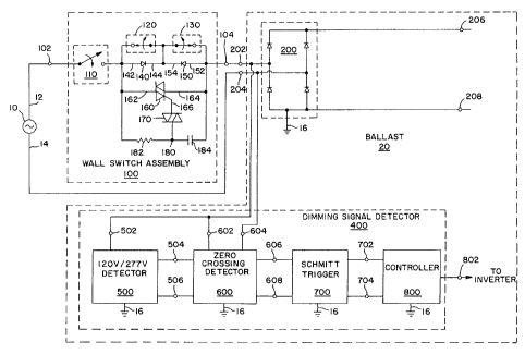
FIG. 1 describes a dimming control system that includes a wall switch
assembly and a ballast having a dimming signal detector circuit, in accordance
with a preferred embodiment of the present invention.
FIG. 2 describes the AC voltage provided to the ballast under different
conditions during the operation of the wall switch assembly illustrated in
FIG. 1.
FIG. 3 describes a 120V/277V detector circuit that is part of the
dimming signal detector circuit illustrated in FIG. 1, in accordance with a
preferred embodiment of the present invention.
FIG. 4 describes a zero crossing detector circuit that is part of the
dimming signal detector circuit illustrated in FIG. 1, in accordance with a
preferred embodiment of the present invention.
FIG. 5 describes a Schmitt trigger circuit that is part of the dimming
signal detector circuit illustrated in FIG. 1, in accordance with a preferred
embodiment of the present invention.
FIG. 6 describes a controller circuit that is part of the dimming signal
detector circuit illustrated in FIG. 1, in accordance with a preferred
embodiment
of the present invention.
CA 02429789 2003-05-23
4
Detailed Description of the Preferred Embodiments
In a preferred embodiment of the present invention, as described in FIG.
1, a dimming control system comprises a wall switch assembly 100 and at least
one electronic ballast 20 that includes a full-wave diode bridge 200 and a
dimming signal detector 400. Wall switch assembly 100 has a first end 102 and
a second end 104. Wall switch assembly 100 is intended for connection in
series with a conventional alternating current (AC) source 10 (e.g., 120 volts
at
60 hertz) having a hot lead 12 and a neutral lead 14. First end 102 is coupled
to
the hot lead 12 of AC source 10. Second end 104 is coupled to a first input
terminal 202 of ballast 20. A second input terminal 204 of ballast 20 is
coupled
to the neutral lead 14 of AC source 10. The ground reference for the circuitry
in
ballast 20 is designated as ground 16.
Dimming signal detector 400 is coupled to the first and second input
terminals 202,204 of ballast 20, and includes an output 802 for connection to
the
ballast inverter (not shown). Dimming signal detector 400 is itself situated
within ballast 20. Wall switch assembly 100 is intended to be situated
external
to the ballast(s), and preferably within an electrical switchbox. If multiple
dimming ballasts are involved, each ballast will have its own dimming signal
detector 400. On the other hand, only one wall switch assembly 100 is required
even if multiple ballasts are involved.
Wall switch assembly 100 includes a first switch 120, a second switch
130, a first diode 140, a second diode 150, a controllable bi-directional
conductive device 160, a voltage-triggered device 170, a triggering resistor
182,
and a triggering capacitor 184. Wall switch assembly 100 may also include a
conventional on-off switch 110 for controlling application of AC power to at
least one ballast connected downstream from wall switch assembly 100. First
diode 140 has an anode 142 and a cathode 144; anode 142 is coupled to first
end
102 via on-off switch 110. Second diode 150 has an anode 152 and a cathode
154; anode 152 is coupled to second end 104, and cathode 154 is coupled to
cathode 144 of diode 140. Switch 120 is coupled in parallel with diode 140,
while switch 130 is coupled in parallel with diode 150. Controllable bi-
CA 02429789 2003-05-23
directional device 160 is preferably implemented as a triac having conduction
terminals 162,164 and a gate terminal 166. Conduction terminal 162 is coupled
to the anode 142 of first diode 140. Conduction terminal 164 is coupled to the
anode 152 of second diode 150. Voltage triggered device 170 is preferably
5 implemented as a diac that is coupled between a node 180 and the gate
terminal
166 of triac 160. Triggering resistor 182 is coupled between the anode 142 of
first diode 140 and node 180. Triggering capacitor 184 is coupled between node
180 and the anode 152 of second diode 150.
Switches 120,130 are preferably implemented as single-pole single-
throw (SPST) switches that are normally closed and that will remain open for
only as long as they are depressed by a user. Moreover, it is desirable that
switches 120,130 be mechanically "ganged" so as to preclude the possibility of
both switches being open at the same time. Preferably, switches 120,130 share
a
single three-position control lever with an up-down action wherein an up
motion
would open switch 120, a down motion would open switch 130, and both
switches 120,130 would be closed at rest. For example, switches 120,130 may
be realized via an "up arrow / down arrow" rocker type arrangement, where
switch 120 is opened while the "up arrow" is depressed, switch 130 is opened
while the "down arrow" is depressed, and both switches 120,130 are closed in
the absence of any depression by a user.
During operation, when on-off switch 110 is in the on position, wall
switch assembly 100 behaves as follows, with reference to FIGs. 1 and 2.
When both switches 120,130 are closed, diodes 140,150 are each
bypassed by their respective switch, so first end 102 is simply shorted to
second
end 104. Thus, both the positive and the negative half cycles of the voltage
from AC source 10 are allowed to pass through unaltered, and the voltage
between ballast input terminals 202,204 (referred to as V202,204 in FIG. 2) is
a
normal sinusoidal AC voltage.
When switch 120 is open and switch 130 is closed, positive-going
current is allowed to proceed (from left to right) into first end 102, through
diode 140, through switch 130 (bypassing diode 150, which blocks positive-
going current), and out of second end 104. Thus, the positive half-cycle of
the
CA 02429789 2003-05-23
6
AC line voltage is allowed to pass through unaltered. The negative half-cycle
of
the AC voltage passes through via triac 160 (bypassing diode 140, which blocks
negative-going current), but in a truncated manner. More specifically, the
leading edge of the negative half-cycle (i.e., the portion between tl and t2
in FIG.
2) will be blocked by triac 160. At time t1, triac 160 is off and will remain
off
until such time as sufficient voltage develops across capacitor 184 in order
to
trigger diac 170 and turn on triac 160. Between ti and t2, the voltage across
capacitor 184 increases as the AC line voltage becomes increasingly negative.
At time t2, the voltage across capacitor 184 reaches a level high enough
(i.e., the
breakover voltage of diac 170) to trigger diac 170 and turn on triac 160.
Thus,
with switch 120 open and switch 130 closed, the voltage provided by wall
switch assembly 100 to ballast input terminals 202,204 is a substantially
sinusoidal AC voltage in which the positive half-cycle is unaltered and the
leading edge of the negative half-cycle is truncated.
When switch 120 is closed and switch 130 is open, negative-going
current is allowed to proceed (from right to left) into second end 104,
through
diode 150, through switch 120 (thus bypassing diode 140, which blocks
negative-going current), and out of first end 102. Thus, the negative half-
cycle
of the AC line voltage is allowed to pass through unaltered. The positive half-
cycle of the AC voltage passes through via triac 160 (bypassing diode 150,
which blocks positive-going current), but in a truncated manner. More
specifically, the leading edge of the positive half-cycle (i.e., the portion
between
t3 and t4 in FIG. 2) will be blocked by triac 160. At time t3, triac 160 is
off and
will remain off until such time as sufficient voltage is applied to gate
terminal
166 in order to turn the device on. Between t3 and t4, the voltage across
capacitor 184 increases as the AC line voltage becomes increasingly positive.
At time t4, the voltage across capacitor 184 reaches a level high enough
(i.e., the
breakover voltage of diac 170) to trigger diac 170 and turn on triac 160.
Thus,
with switch 120 closed and switch 130 open, the voltage provided by wall
switch assembly 100 to ballast input terminals 202,204 is a substantially
sinusoidal AC voltage in which the leading edge of the positive half-cycle is
truncated and the negative half-cycle is unaltered.
CA 02429789 2003-05-23
7
Preferably, the time periods ti to t2 and t3 to t4 are selected to be quite
short in comparison with the duration of one half-cycle of the AC line
voltage,
so as to preclude any negative effects regarding the line regulation of the
boost
converter in ballast 20. The duration of the time periods ti to t2 and t3 to
t4 is
determined by the breakover voltage of diac 170, the values of resistor 182
and
capacitor 184, and the magnitude of the AC line voltage.
Preferably, dimming signal detector 400 treats a depression of switch
130 (i.e., truncated positive half-cycle) as a "brighten" command and responds
by increasing the level or duty cycle of its output voltage (i.e., the voltage
at
output 802) during the time that switch 130 remains depressed. Conversely, a
depression of switch 120 (i.e., truncated negative half-cycle) is treated as a
"dim" command, to which dimming signal detector 400 responds by decreasing
the level or duty cycle of its output voltage. Alternatively, dimming signal
detector 400 may be designed so that the aforementioned logic convention is
reversed; that is, dimming signal detector 400 may be designed such that
truncation of the positive half-cycle is treated as a "dim" command, while
truncation of the negative half-cycle treated as a "brighten" command.
In contrast with prior art "line control" dimming approaches, such as
those that employ a triac in series with the AC source, wall switch assembly
100
introduces no line-conducted electromagnetic interference (EMI) or distortion
in
the AC line current during normal operation (i.e., when switches 120,130 are
closed). Moreover, wall switch assembly 100 dissipates no power during
normal operation because the AC current drawn by any ballast(s) connected
downstream flows through switches 120,130 rather than diodes 140,150. On the
other hand, when one of the switches 120,130 is opened in order to send a
"dim"
or "brighten" signal, a small amount of power will be dissipated in one of the
diodes 140,150 and in triac 160, but only for as long as the switch remains
depressed. The required power rating of the diodes and the triac is dictated
by
the power that will be drawn by the ballast(s) connected downstream.
CA 02429789 2003-05-23
8
Referring again to FIG. 1, in a preferred embodiment of the present
invention, dimming signal detector 400 includes a 120V/277V detector circuit
500, a zero crossing detector circuit 600, a Schmitt trigger circuit 700, and
a
controller circuit 800. 120V/277 V detector 500 includes an input 502 coupled
to either input terminal 202,204 of ballast 20, and a pair of outputs 504,506
coupled to zero crossing detector 600. The function of 120V/277V detector
circuit is to ensure that zero crossing detector 600 deals with essentially
the
same voltage levels, regardless of the actual AC line voltage. Zero crossing
detector 600 includes a first input 602, a second input 604, and a pair of
outputs
606,608. First input 602 is coupled to the first input terminal 202 of ballast
20.
Second input 204 is coupled to the second input terminal 204 of ballast 20.
Outputs 606,608 are coupled to Schmitt trigger 700. The function of zero
crossing detector 600 is to detect the presence of a "dim" or "brighten"
command, and to adjust the duty cycles of the signals at outputs 626,656
accordingly. Schmitt trigger 700 includes a pair of outputs 702,704 coupled to
controller 800. The function of Schmitt trigger is to receive the variable
duty
DC signals provided by zero crossing detector 600 and provide digitized output
signals (i.e., corresponding to a logic "1" or logic "0") to controller 800.
Controller 800 has an output 802. The function of controller is to provide a
variable signal at output 802 wherein, preferably, the duty cycle of the
signal is
increased in response to a "brighten" command and decreased in response to a
"dim" command. Preferred structures for 120V/277V detector 500, zero
crossing detector 600, Schmitt trigger 700, and controller 800 are described
herein with reference FIGs. 3-6.
As alluded to previously, output 802 is intended for connection to the
ballast inverter. The voltage level or the duty cycle of the signal provided
at
output 802 is varied in dependence on the signals provided by wall switch
assembly 100, and can be used to control the inverter operating frequency or
duty cycle, and hence the amount of current provided to the lamp(s), in any of
a
number of ways that are well-known to those skilled in the art. An example of
a ballast that provides dimming through control of the inverter operating
CA 02429789 2010-11-25
9
frequency is disclosed in U.S. Pat. No. 5,457,360.
Preferably, dimming signal detector 400 provides a low voltage, variable duty
cycle
voltage signal at output 802. As described herein with reference to controller
circuit 800 and
FIG. 8, the voltage signal at output 802 is a variable duty cycle squarewave
signal with a
peak value of about 5 volts, a minimum value of zero volts, and a duty cycle
that can be
varied (in dependence on the dimming commands from wall switch assembly 100)
between
about 4.44% (preferably, corresponding to an extreme "dim" setting) and about
95.6%
(preferably, corresponding to an extreme "brighten" setting).
Upon initial application of AC power to ballast 20, the duty cycle of the
signal at
output 802 will, preferably, be at its maximum value. When a "dim" command is
issued via
wall switch assembly 100 (i.e., when a truncated negative half-cycle is
detected), dimming
signal detector 400 will reduce the duty cycle by a small amount. As
successive "dim"
commands are sent, the duty cycle will be reduced by a small amount for each
truncated
negative half-cycle that is detected. If "dim" commands continue to be sent,
the duty cycle
will eventually reach its minimum value and will remain at that value until
such time as a
"brighten" command is sent. Similarly, upon receipt of a "brighten" command
(i.e.,
detection of a truncated positive half-cycle), dimming signal detector 400
will increase the
duty cycle by a small amount. As successive "brighten" commands are sent, the
duty cycle
will be increased by a small amount for each truncated positive half-cycle
that is detected. If
"brighten" commands continue to be sent, the duty cycle will eventually reach
its maximum
value and will remain at that value until such time as a "dim" command is
sent.
A preferred embodiment of dimming signal detector 400 is now explained with
reference to FIGS. 3-6 as follows.
Referring to FIG. 3, in a preferred embodiment of the present invention,
120V/277V
detector 500 has the following structure and operation. Resistors 510,512
function as a
voltage divider for providing a scaled-down version of the AC line voltage to
the positive
input 524 of comparator 520. Resistors 510,512 are sized such that, for an AC
line voltage
of 120 volts (rms), the voltage
CA 02429789 2003-05-23
provided to the positive input 524 of comparator 520 will be 4.5 volts.
Capacitor 514 serves as a filter capacitor for reducing the low frequency
ripple
that would otherwise be present in the voltage across resistor 512. Resistors
516,518 are sized so as to bias the inverting input 522 of comparator 520 at
6.0
5 volts when VCC is set at 14.0 volts. Resistors 530,532 serve as current-
limiting
resistors for limiting the current that is provided to the gates of
transistors
540,560 when the output 526 of comparator 520 goes high.
For an AC line voltage of 120 volts (rms), the voltage at positive input
524 (i.e., 4.5 volts) will be less than the voltage at negative input 522
(i.e., 6.0
10 volts), so the voltage at comparator output 526 will be zero and,
consequently,
transistors 540,560 will both be off.
For an AC line voltage of 277 volts (rms), the voltage at positive input
524 will be at about 10.4 volts, which is greater than the voltage at negative
input 522 (i.e., 6.0 volts). As a result, the voltage at comparator output 526
will
go high and turn on both transistors 540,560. With transistors 540 on,
resistor
550 is effectively placed in parallel with resistor 612 (see FIG. 4) in zero
crossing detector 600. With transistor 560 on, resistor 570 is effectively
placed
in parallel (via output 506) with resistor 642 (see FIG. 4) in zero crossing
detector 600. Consequently, and referring again to FIG. 4, the voltages that
are
provided to the positive inputs 624,654 of comparators 620,650 will be
proportionately scaled down when the AC line voltage is 277 volts rather than
120 volts. In this way, 120V/277V detector 500 ensures that the signals within
zero crossing detector 600 are essentially the same, regardless of whether the
AC line voltage is 120 volts or 277 volts.
Referring now to FIG. 4, in a preferred embodiment of the present
invention, zero crossing detector 500 has the following structure and
operation.
Resistors 610,612 function as a voltage divider for providing a scaled-down
version of the positive half-cycles (of the AC voltage supplied to the
ballast) to
the positive input 624 of comparator 620. As previously described with
reference to FIG. 3, when the AC line voltage is 277 volts (rms), 120V/277V
detector circuit 500 effectively places an additional resistance (i.e.,
resistor 550
in FIG. 3) in parallel with resistor 612 so as to further scale down the
voltage
CA 02429789 2003-05-23
11
provided to the positive input 624 of comparator 620. Similarly, resistors
640,642 function as a voltage divider for providing a scaled-down version of
the
negative half-cycles (of the AC voltage supplied to the ballast) to the
positive
input 654 of comparator 650. As previously described with reference to FIG. 3,
when the AC line voltage is 277 volts (rms), 120V/277V detector circuit 500
effectively places an additional resistance (i.e., resistor 570 in FIG. 4) in
parallel
with resistor 642 so as to further scale down the voltage provided to the
positive
input 654 of comparator 650.
During operation, the positive and negative half-cycles of the AC voltage
supplied to ballast 20 are compared with one volt reference voltages provided
at
the negative inputs 622,652 of comparators 620,650. The one volt reference
voltages are derived from Vcc through voltage dividers formed by resistors
616,618 and resistors 646,648. Alternatively, resistors 646,648 may be
omitted,
and the one volt reference voltage for comparator 650 can be provided simply
by connecting the negative input 652 of comparator 650 to the negative input
622 of comparator 620 (in which case resistors 616,618 provide the one volt
reference voltage for both comparators 620,650). Resistors 628,658 function as
pull-up resistors for biasing the outputs 626,656 of comparators 620,650.
The signals provided at the outputs 626,656 of comparators 620,650 are
approximately squarewave voltages with a duration that decreases if a
truncated
portion is present in the signals provided to positive inputs 624,654. More
specifically, if the positive half-cycle is not truncated, the signal at the
output
626 of comparator 620 will be a squarewave with the duration of the nonzero
portion equal to about 7.7 milliseconds; if, on the other hand, the positive
half-
cycle is truncated, the signal at the output of comparator 620 will be a
squarewave with the duration of the nonzero portion equal to less than 7.7
milliseconds. Along similar lines, if the negative half-cycle is not
truncated, the
signal at the output 656 of comparator 650 will be a squarewave with the
duration of the nonzero portion equal to about 7.7 milliseconds; if, on the
other
hand, the negative half-cycle is truncated, the signal at the output 656 of
comparator 650 will be a squarewave with the duration of the nonzero portion
equal to less than 7.7 milliseconds. In this way, zero crossing detector 600
CA 02429789 2003-05-23
12
provides outputs that indicate whether or not a "dim" or "brighten" signal has
been sent from wall switch assembly 100.
The outputs of comparators 620,650 are filtered through RC filters in
order to provide corresponding voltages at outputs 606,608. More specifically,
the output of comparator 620 is filtered through an RC filter formed by
resistor
630 and capacitor 632, while the output of comparator 650 is filtered through
an
RC filter formed by resistor 660 and capacitor 662. If a truncated positive
half-
cycle is detected, the voltage at output 606 will be correspondingly lower
than it
would be if no truncated positive half-cycle is detected. Similarly, if a
truncated
negative half-cycle is detected, the voltage at output 608 will be
correspondingly
lower than it would be if no truncated negative half-cycle is detected.
Referring now to FIG. 5, in a preferred embodiment of the present
invention, Schmitt trigger 700 has the following structure and operation.
Resistors 710,712 and resistors 740,742 serve as voltage dividers for
providing
appropriate reference voltages at the positive inputs 724,754 of comparators
720,750. Resistors 728,758 are pull-up resistors for appropriately biasing
outputs 726,756 of comparators 720,750. Resistors 730,760 provide positive
feedback from outputs 726,756 to positive inputs 724,754. Negative inputs
722,752 are coupled to corresponding outputs from zero crossing detector 600,
which was previously described with reference to FIG. 4. The outputs 726,756
of comparators 720,750 are coupled to outputs 702,704 of Schmitt trigger 700.
During operation, for both comparators 720,750, as long as the voltage
at the negative input (722 or 752) is greater than the reference voltage at
the
positive input (724 or 754), the output voltage at the comparator output (726
or
756) will be low. Once the voltage at the negative input becomes less than the
voltage at the positive input, the voltage at the comparator output will go
high.
Because positive feedback is provided (via resistors 730,760), when the
voltage
at the comparator output goes high, that causes the reference voltage at the
positive input to increase. Thus, as long as the ripple in the voltage at the
negative input is less than the change in the reference voltage, the output
voltage
will be stable.
CA 02429789 2003-05-23
13
Under normal operation, when neither a "dim" nor a "brighten"
command has been sent, the voltages at positive inputs 724,754 are less than
the
reference voltages at negative inputs 722,752. Consequently, the voltages at
comparator outputs 726,756 will be low. When a "brighten" command is sent,
the DC voltage provided at output 606 of zero crossing detector 600 will
decrease. Correspondingly, the voltage at negative input 722 of comparator 720
will decrease to a level that is less than the reference voltage at positive
input
724, causing the voltage at output 726 to go high. Once the "brighten"
command ceases to be sent, the voltage at output 726 will go back to being
low.
Along similar lines, when a "dim" command is sent, the DC voltage provided at
output 608 of zero crossing detector 600 will decrease. Correspondingly, the
voltage at negative input 752 of comparator 750 will decrease to a level that
is
less than the reference voltage at positive input 754, causing the voltage at
output 756 to go high. Once the "dim" command ceases to be sent, the voltage
at output 756 will go back to being low.
In this way, Schmitt trigger 700 provides digital output signals at outputs
702,704 that indicate whether or not a "dim" or "brighten" command has been
received.
Referring now to FIG. 6, in a preferred embodiment of the present
invention, controller 800 has the following structure and operation. Resistors
820,822,824,826 form a voltage divider from the outputs 702,704 of Schmitt
trigger 700 to the inputs 812,814 of microcontroller 810. Microcontroller 810
may be implemented using any of a number of suitable devices, such as the
PICI2C509A 8-bit CMOS microcontroller manufactured by Microchip
Technology Inc. Microcontroller 810 is configured to provide at output 816
(and, thus, at output 802) a variable duty cycle squarewave signal, wherein
the
duty cycle is adjusted in dependence on the signals provided to inputs
812,814.
Preferably, the duty cycle is variable between a minimum of about 4.44% and a
maximum of about 95.6%. It is further preferred that, upon initial application
of
power, the duty cycle will be set at its maximum value (which, in a preferred
arrangement, correspond to a maximum light output setting).
CA 02429789 2003-05-23
14
Input 812 is configured to serve as a "brighten" input, while input 814
serves as a "dim" input. During operation, when no "dim" or "brighten"
command has been sent, the signals at inputs 812,814 will both be a logic "0."
Under such a condition, the duty cycle of the signal at output 816 will remain
unchanged.
When a "dim" command is sent from wall switch assembly 100, the
signal at input 812 will be a logic "0" and the signal at input 814 will be a
logic
"1." Under this condition, microcontroller 810 will decrease the duty cycle of
the signal at output 816. If successive "dim" commands are received (e.g., if
switch 120 remains open for a sustained period of time, such as one second),
microcontroller 810 will continue to incrementally decrease the duty cycle all
the way down to the point of reaching the minimum duty cycle (e.g., 4.44%).
Once the minimum duty cycle is reached, any further "dim" commands will
have no effect on the duty cycle of the signal provided at output 802.
When a "brighten" command is sent from wall switch assembly 100, the
signal at input 812 will be a logic "1" and the signal at input 814 will be a
logic
"0." Correspondingly, microcontroller 810 will increase the duty cycle of the
signal at output 816. If successive "brighten" commands are received (e.g., id
switch 130 remains open for a sustained period of time, such as one second),
microcontroller 810 will continue to incrementally increase the duty cycle all
the
way up to the point of reaching the maximum duty cycle (e.g., 95.6%). Once
the maximum duty cycle is reached, any further "brighten" commands will have
no effect on the duty cycle of the signal provided at output 802.
As previously discussed with regard to wall switch assembly 100 (see
FIG. 1), it is preferred that switches 120,130 be "ganged" so as to preclude
the
possibility of both switches being open at the same time. Nevertheless, even
if
switches 120,130 were to be opened at the same time (i.e., if both a "dim" and
"brighten" command were sent at the same time), microcontroller 810 is
preferably configured to treat such a condition in the same manner as if
neither a
"dim" command nor a "brighten" command were sent. More specifically,
microcontroller 810 is preferably configured so as to treat the simultaneous
CA 02429789 2011-04-01
occurrence of a logic "1" at both inputs 812,814 in the same manner as the
simultaneous
occurrence of a logic "0" at both inputs 812,814.
In this way, wall switch assembly 100 and dimming signal detector 400 provide
a
variable duty cycle control voltage that can be provided to the ballast
inverter in order to
5 effect dimming of the lamp(s) connected to the ballast output.
While the preceding description has discussed "dim" and "brighten" commands
that
originate via user manipulation of switches 120,130 of wall switch assembly
100 (see FIG. 1),
it should be appreciated that dimming signal detector 400 is likewise capable
of receiving
those commands directly from the electric utility company. For instance, the
utility company
10 may itself implement a "load shedding" protocol wherein the utility company
provides a
"dim" command simply by truncating a predetermined number of negative half-
cycles of the
AC line voltage. Dimming signal detector 400 will detect the truncated
negative half-cycles
and adjust its output in the same manner as it does in response to a series of
"dim" commands
sent via the momentary opening of switch 120. At the end of the "load
shedding" period (e.g.,
15 once the power demand experienced by the electrical utility has decreased
sufficiently to
obviate the need for load shedding), the utility company may provide a
"brighten" command
simply by truncating a series of positive half-cycles of the AC line voltage.
Dimming signal
detector 400 will detect the truncated positive half-cycles and adjust its
output in the same
manner as it does in response to a series of "brighten" commands sent via the
momentary
opening of switch 120. Thus, in addition to the other benefits previously
discussed herein, the
present invention easily accommodates load shedding strategies.
Although the present invention has been described with reference to certain
preferred
embodiments, numerous modifications and variations can be made by those
skilled in the art
without departing from the scope of this invention.