Language selection

Search

Patent 2430326 Summary

Third-party information liability

Some of the information on this Web page has been provided by external sources. The Government of Canada is not responsible for the accuracy, reliability or currency of the information supplied by external sources. Users wishing to rely upon this information should consult directly with the source of the information. Content provided by external sources is not subject to official languages, privacy and accessibility requirements.

Claims and Abstract availability

Any discrepancies in the text and image of the Claims and Abstract are due to differing posting times. Text of the Claims and Abstract are posted:

  • At the time the application is open to public inspection;
  • At the time of issue of the patent (grant).
(12) Patent: (11) CA 2430326
(54) English Title: METHOD AND DEVICE FOR REGULATING THE POWER OF MILLIMETER WAVES FOR A V-BAND TR MODULE
(54) French Title: PROCEDE ET DISPOSITIF DE REGULATION DE PUISSANCE DES ONDES MILLIMETRIQUES POUR UN MODULE TR BANDE V
Status: Deemed expired
Bibliographic Data
(51) International Patent Classification (IPC):
  • H01P 1/22 (2006.01)
  • H03G 3/30 (2006.01)
(72) Inventors :
  • FILLEBOCK, MARION (Germany)
  • SCHROTH, JOERG (Germany)
(73) Owners :
  • EADS DEUTSCHLAND GMBH (Germany)
(71) Applicants :
  • EADS DEUTSCHLAND GMBH (Germany)
(74) Agent: ROBIC
(74) Associate agent:
(45) Issued: 2009-07-28
(86) PCT Filing Date: 2001-11-09
(87) Open to Public Inspection: 2002-06-13
Examination requested: 2004-09-02
Availability of licence: N/A
(25) Language of filing: English

Patent Cooperation Treaty (PCT): Yes
(86) PCT Filing Number: PCT/DE2001/004215
(87) International Publication Number: WO2002/047245
(85) National Entry: 2003-05-28

(30) Application Priority Data:
Application No. Country/Territory Date
100 60 332.7 Germany 2000-12-04

Abstracts

English Abstract


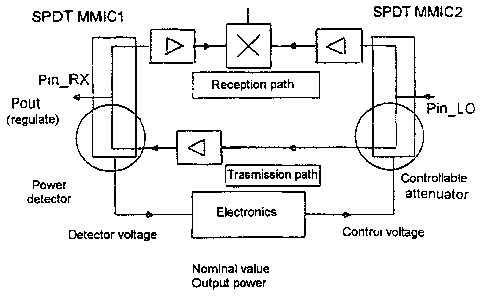
The invention relates to a method for regulating the power of millimetre waves
for a V-band TR module. According to said method, the power output is detected
and regulated at a constant level with a regulating electronics system, by
means of a damping member. The invention provides that for transmission, for
operation at a frequency in the 60 GHz range and higher, a first SPDT (single
pole double throw) MMIC switch is used as a regulated damping member and a
second SPDT MMIC switch which acts as a transmit-receive changeover switch is
used as a power output detector. For reception, both SPDTs are used as
switches. Overall, the power regulation for the entire TR module results in an
increase of the module yield through compensation of chip leakage and
temperature effects. The multiple use of the SPDT MMICs as switches, damping
member and power detector saves costs.


French Abstract

Dans un procédé de régulation de puissance des ondes millimétriques dans le cas d'un module TR bande V, on détecte la puissance de sortie et on la règle à un niveau constant par une électronique de réglage à l'aide d'un atténuateur. Selon l'invention, en mode émission à une fréquence d'au moins 60 GHz, on utilise un premier interrupteur unipolaire à deux directions (SPDT) MMIC comme atténuateur réglable et un deuxième interrupteur SPDT MMIC servant de commutateur émission-réception comme détecteur de puissance de sortie. En mode réception, on utilise les deux interrupteurs SPDT comme commutateurs. Globalement, le réglage de puissance de tout le module TR permet d'augmenter le rendement du module par compensation de la dispersion de la puce et d'obtenir des effets de température. L'utilisation multiple des interrupteurs SPDT MMIC comme commutateurs, atténuateurs et détecteurs de puissance permet de réduire les coûts.

Claims

Note: Claims are shown in the official language in which they were submitted.


6

WHAT IS CLAIMED IS:


1. Method to control the power of millimetric waves for a V-band TR module at
a
frequency in the range of 50 GHz and higher, the method comprising the acts of

separating the transmission and receiving path via two SPDT (single pole
double
throw) MMIC switches, for the transmission, the first SPDT MMIC switch as a
variable attenuator and the second SPDT MMIC switch as a detector for the
output
power; and by way of an electronic control circuit, the control of the output
power to a
defined level is achieved.


2. Device to control the power of millimetric waves for a V-band TR module at
a
frequency in the range of 50 GHz and higher, comprising: two SPDT (single pole

double throw) MMIC switches for separating the transmit and receive path;
wherein
for transmission, the first SPDT MMIC switch is used as a variable attenuator
and the
second SPDT MMIC switch is used as a detector for the output power, and an
electronic unit to control the output power; wherein in the case of the SPDT
MMIC
having two switch arms, on each switch arm, two parallel-connected diode
pairs,
respectively are connected between the RF line and ground, and wherein, in
operation as a power detector, one arm is blocked and the second arm is
switched
via a bias voltage of 0 V to conducting, and further wherein the RF power
flowing
through the latter arm is rectified at the diodes, and the measurable
rectified voltage
is used as a measurement for the transmitted power.


3. Device to control the power of millimetre waves for a V-band TR module at a

frequency in the range of 50 GHz and higher, comprising: two SPDT (single pole

double throw) MMIC switches for separating the transmit and receive path;
wherein
for transmission, the first SPDT MMIC switch is used as a variable attenuator
and the
second SPDT MMIC switch is used as a detector for the output power; and an
electronic unit to control the output power; wherein in the case of the SPDT
MMIC


7

having two switch arms, in switch mode, an input power at the IN port can
optionally
be switched to the O1 or O2 port, and wherein, in a mode as a variable
attenuator,
the O2 port is terminated in a reflection free manner and a variable
attenuation can
be set between the IN and O1 port by variation of the supply voltage.

Description

Note: Descriptions are shown in the official language in which they were submitted.


CA 02430326 2009-01-28
1

METHOD AND DEVICE FOR REGULATING THE POWER OF MILLIMETER
WAVES FOR A V-BAND TR MODULE

The invention relates to a method and a device for regulating the power of
millimetric
waves in a V-band TR module.

Particularly in mobile communications devices, the
output power should be as constant as possible, to be
precise irrespective of individual characteristics of
the components and appliances which are produced in
large quantities. Controllable attenuators are produced
on MMICs with PIN diodes or as MESFET switches for
frequencies below 50 GHz. Other power regulation
concepts for lower frequencies are also known from the
prior art. However, no V-band TR module with a
regulated output power is currently known. Furthermore,
no controllable attenuator for 60 GHz is currently
commercially available as an MMIC.
The individual adjustment of manufactured appliances is
highly costly; it would therefore be desirable to avoid
this by appropriate design. A further aim at the same
time is that as few additional components as possible
should be required since, on the one hand, they
themselves once again have individual scatters and, on
the other hand, result in costs.

The company United Monolithic Semiconductors S.A.S.,
91401 Orsay Cedex France offer a 50-60 GHz SPDT
(= Single Pole Double Throw) switch for communication
systems with the type designation "CHS2190a", which has


CA 02430326 2009-01-28
2

already been used as a transmission/reception
changeover switch in transmission/reception modules.
The aim of the invention is to use this or a
corresponding switch to provide power regulation with
said features.

According to one aspect of the invention, there is provided a method to
control the
power of millimetric waves for a V-band TR module at a frequency in the range
of 50
GHz and higher, the method comprising the acts of: separating the transmission
and
receiving path via two SPDT (single pole double throw) MMIC switches, for the
transmission, the first SPDT MMIC switch as a variable attenuator and the
second
SPDT MMIC switch as a detector for the output power; and by way of an
electronic
control circuit, the control of the output power to a defined level is
achieved.

Another aspect of the invention concerns a device to control the power of
millimetric
waves for a V-band TR module at a frequency in the range of 50 GHz and higher,
comprising: two SPDT (single pole double throw) MMIC switches for separating
the
transmit and receive path; wherein for transmission, the first SPDT MMIC
switch is
used as a variable attenuator and the second SPDT MMIC switch is used as a
detector for the output power, and an electronic unit to control the output
power;
wherein in the case of the SPDT MMIC having two switch arms, on each switch
arm,
two parallel-connected diode pairs, respectively are connected between the RF
line
and ground, and wherein, in operation as a power detector, one arm is blocked
and
the second arm is switched via a bias voltage of 0 V to conducting, and
further
wherein the RF power flowing through the latter arm is rectified at the
diodes, and the
measurable rectified voltage is used as a measurement for the transmitted
power.

Yet another aspect of the invention concerns a device to control the power of
millimetre waves for a V-band TR module at a frequency in the range of 50 GHz
and
higher, comprising: two SPDT (single pole double throw) MMIC switches for
separating the transmit and receive path; wherein for transmission, the first
SPDT


CA 02430326 2009-01-28
2a

MMIC switch is used as a variable attenuator and the second SPDT MMIC switch
is
used as a detector for the output power; and an electronic unit to control the
output
power; wherein in the case of the SPDT MMIC having two switch arms, in switch
mode, an input power at the IN port can optionally be switched to the 01 or 02
port,
and wherein, in a mode as a variable attenuator, the 02 port is terminated in
a
reflection free manner and a variable attenuation can be set between the IN
and 01
port by variation of the supply voltage.

The use of a SPDT MMIC as a controllable attenuator
makes it possible to set a desired transmission power
and to compensate for scatters between the chips. This
forms the core component for power regulation (control
element). The double function of the chip results in
considerable cost savings.

The use of the second SPDT MMIC as a power detector
also results in costs being saved, owing to the double
function.

Overall, the power regulation for the entire TR module
leads to an increase in the module yield by
compensation for scatters between chips and temperature
effects. The multiple use of the SPDT MMICs as
switches, as an attenuator and as a power detector
leads to the stated advantages.

Details of the invention can be found in the dependent
claims and in the description, in which one exemplary
embodiment is described with reference to the drawing,
in which:


CA 02430326 2009-01-28
2b

Figure 1 shows a block diagram of the transmission
power regulation according to the invention,
Figure 2 shows the layout and the pad designations for
the known SPDT MMIC,

Figure 3 shows the outline circuit diagram,

Figure 4 shows the external circuitry and the DC
supply,


CA 02430326 2003-05-28

WO 02/47245 - 3 - PCT/DE01/04215
Figure 5 shows the attenuation response as a function
of the monitor voltage,

Figure 6 shows the use of the SPDT MMIC as a detector,
and

Figure 7 shows the maximum available and regulated
transmission power.

According to the invention, the known MMIC may be
operated either as a Schottky diode switch of the SPDT
(Single Pole Double Throw) type or, by different supply
voltages, as a controllable attenuator. Figures 2 and 3
show the layout of the SPDT MMIC and an outline circuit
diagram. During switching operation, the input power of
the port IN is passed on either to the port 01 or 02.
For operation as a variable attenuator, the port 02 is
terminated without any reflection, and the switching
arm IN-02 is operated in the forward-biased direction.
A variable attenuation of between 3.5 and 25 dB can be
produced between the ports IN and 01, via the DC supply
voltage (see Figures 4 and 5).

Figure 4 shows the external circuitry and a DC supply.
The operating modes are as follows:

Switching operation:
Switching arm IN-01 in the ON state, switching arm IN-
02 in the OFF state:
Pads A1,A2: -2.5 V
Pads B1,B2: 12 mA
OFF-state: switching arm switched off
ON-state: switching arm switched on

The external supply voltage is provided via series
resistors of about 250 ohms in series with the pads
Al, A2, Bl, B2.


CA 02430326 2003-05-28

WO 02/47245 - 4 - PCT/DE01/04215
Detector operation:

Switching arm IN-O1 as a detector, switching arm IN-02
in the OFF state:
Pads A1,A2: 0 V, (1 kohm in series with pads)
Pads B1,B2: 12 mA

Operation as a variable attenuator:

Switching arm IN-Ol in the ON state (port 01 terminated
without any reflections),
Switching arm IN-02 in the attenuation mode:
Pads A1,A2: -2.5 V
Pads B1,B2: 0-12 mA (corresponds to 0-4 V across
the series resistance of 250 ohms)

Two diode pads 4/5 and 6/7 are connected between the RF
line and ground on each switching arm on the SPDT MMIC.
When the SPDT MMIC is being operated as a power
detector, one arm is switched off (for example IN-02),
while the second arm is switched on with a bias voltage
of 0 V. The RF power flowing through the ON arm is
rectified by the parallel-connected diodes. The control
voltage which can be measured on the pads Al and A2 is
a measure of the power flowing through, as is shown in
Figure 6. The control voltage on the pad A2 is used for
the power measurement. An SPDT MMIC can be used for
power detection for levels of 3 dBM<P<10 dBm.

Figure 5 shows the attenuation response as a function
of the monitor voltage. In this case, the values are as
follows:

DC circuitry and voltage supply:
Pads A1,A2: -2.5 V
Pads B1,B2: monitor voltage applied across a
250 ohm series resistance.


CA 02430326 2003-05-28

WO 02/47245 - 5 - PCT/DE01/04215
RF configuration

Measurement on the wafer sample at 58 GHz
Input power at the port IN, output power at the port
02, port 01 was terminated by a 10 dB attenuator.

Figure 6 shows the use of the SPDT MMIC as a detector.
The diagram shows the detector voltage as a function of
the measured output power. In this case:
DC circuitry and voltage supply:
Pads Al, A2: 0 V supplied via a 1 kohm series
resistance
Pads B1,B2: 12 mA
RF configuration:

Measurement on wafer sample at 58 GHz
Input power at the port 01, output power at the port
IN, port 02 was terminated with a 10 dB attenuator

The transmission power regulation according to the
invention was developed using the described components
for a transmission/reception module, as is shown in
simplified form in the block diagram in Figure 1.
During reception, both SPDT MMICs (1 and 2) are used as
switches. The LO power (Pin_LO) and the reception power
(Pin_RX) are passed to the mixer. During transmission,
the SPDT MMIC 1 acts as a controllable attenuator, and
SPDT MMIC 2 acts as a power detector. The power control
loop is closed via analog electronics. The desired
output value is set on the electronics via the nominal
value.
Figure 7 shows the output power measured at the
spectrum analyzer for the unregulated case (maximum
available power) and for the regulated case
(Pout=5dBm=const).

Representative Drawing
A single figure which represents the drawing illustrating the invention.
Administrative Status

For a clearer understanding of the status of the application/patent presented on this page, the site Disclaimer , as well as the definitions for Patent , Administrative Status , Maintenance Fee  and Payment History  should be consulted.

Administrative Status

Title Date
Forecasted Issue Date 2009-07-28
(86) PCT Filing Date 2001-11-09
(87) PCT Publication Date 2002-06-13
(85) National Entry 2003-05-28
Examination Requested 2004-09-02
(45) Issued 2009-07-28
Deemed Expired 2012-11-09

Abandonment History

There is no abandonment history.

Payment History

Fee Type Anniversary Year Due Date Amount Paid Paid Date
Registration of a document - section 124 $100.00 2003-05-28
Application Fee $300.00 2003-05-28
Maintenance Fee - Application - New Act 2 2003-11-10 $100.00 2003-10-28
Request for Examination $800.00 2004-09-02
Maintenance Fee - Application - New Act 3 2004-11-09 $100.00 2004-10-27
Maintenance Fee - Application - New Act 4 2005-11-09 $100.00 2005-10-24
Maintenance Fee - Application - New Act 5 2006-11-09 $200.00 2006-10-25
Maintenance Fee - Application - New Act 6 2007-11-09 $200.00 2007-10-24
Maintenance Fee - Application - New Act 7 2008-11-10 $200.00 2008-10-23
Final Fee $300.00 2009-05-11
Maintenance Fee - Patent - New Act 8 2009-11-09 $200.00 2009-10-30
Maintenance Fee - Patent - New Act 9 2010-11-09 $200.00 2010-10-28
Owners on Record

Note: Records showing the ownership history in alphabetical order.

Current Owners on Record
EADS DEUTSCHLAND GMBH
Past Owners on Record
FILLEBOCK, MARION
SCHROTH, JOERG
Past Owners that do not appear in the "Owners on Record" listing will appear in other documentation within the application.
Documents

To view selected files, please enter reCAPTCHA code :


To view images, click a link in the Document Description column. To download the documents, select one or more checkboxes in the first column and then click the "Download Selected in PDF format (Zip Archive)" or the "Download Selected as Single PDF" button.

List of published and non-published patent-specific documents on the CPD .

If you have any difficulty accessing content, you can call the Client Service Centre at 1-866-997-1936 or send them an e-mail at CIPO Client Service Centre.


Document
Description 
Date
(yyyy-mm-dd) 
Number of pages   Size of Image (KB) 
Abstract 2003-05-28 2 93
Claims 2003-05-28 2 61
Drawings 2003-05-28 4 91
Description 2003-05-28 5 196
Representative Drawing 2003-07-28 1 10
Cover Page 2003-07-29 1 46
Description 2009-01-28 7 248
Claims 2009-01-28 2 54
Representative Drawing 2009-07-06 1 12
Cover Page 2009-07-06 2 52
PCT 2003-05-28 5 173
Assignment 2003-05-28 6 185
PCT 2003-05-29 2 66
Prosecution-Amendment 2004-09-02 1 25
Prosecution-Amendment 2008-07-31 3 72
Prosecution-Amendment 2009-01-28 10 274
Correspondence 2009-05-11 2 54
Correspondence 2010-08-10 1 47
Correspondence 2011-12-21 1 65