Sélection de la langue

Search

Sommaire du brevet 2430326 

Énoncé de désistement de responsabilité concernant l'information provenant de tiers

Une partie des informations de ce site Web a été fournie par des sources externes. Le gouvernement du Canada n'assume aucune responsabilité concernant la précision, l'actualité ou la fiabilité des informations fournies par les sources externes. Les utilisateurs qui désirent employer cette information devraient consulter directement la source des informations. Le contenu fourni par les sources externes n'est pas assujetti aux exigences sur les langues officielles, la protection des renseignements personnels et l'accessibilité.

Disponibilité de l'Abrégé et des Revendications

L'apparition de différences dans le texte et l'image des Revendications et de l'Abrégé dépend du moment auquel le document est publié. Les textes des Revendications et de l'Abrégé sont affichés :

  • lorsque la demande peut être examinée par le public;
  • lorsque le brevet est émis (délivrance).
(12) Brevet: (11) CA 2430326
(54) Titre français: PROCEDE ET DISPOSITIF DE REGULATION DE PUISSANCE DES ONDES MILLIMETRIQUES POUR UN MODULE TR BANDE V
(54) Titre anglais: METHOD AND DEVICE FOR REGULATING THE POWER OF MILLIMETER WAVES FOR A V-BAND TR MODULE
Statut: Périmé et au-delà du délai pour l’annulation
Données bibliographiques
(51) Classification internationale des brevets (CIB):
  • H01P 01/22 (2006.01)
  • H03G 03/30 (2006.01)
(72) Inventeurs :
  • FILLEBOCK, MARION (Allemagne)
  • SCHROTH, JOERG (Allemagne)
(73) Titulaires :
  • EADS DEUTSCHLAND GMBH
(71) Demandeurs :
  • EADS DEUTSCHLAND GMBH (Allemagne)
(74) Agent: ROBIC AGENCE PI S.E.C./ROBIC IP AGENCY LP
(74) Co-agent:
(45) Délivré: 2009-07-28
(86) Date de dépôt PCT: 2001-11-09
(87) Mise à la disponibilité du public: 2002-06-13
Requête d'examen: 2004-09-02
Licence disponible: S.O.
Cédé au domaine public: S.O.
(25) Langue des documents déposés: Anglais

Traité de coopération en matière de brevets (PCT): Oui
(86) Numéro de la demande PCT: PCT/DE2001/004215
(87) Numéro de publication internationale PCT: DE2001004215
(85) Entrée nationale: 2003-05-28

(30) Données de priorité de la demande:
Numéro de la demande Pays / territoire Date
100 60 332.7 (Allemagne) 2000-12-04

Abrégés

Abrégé français

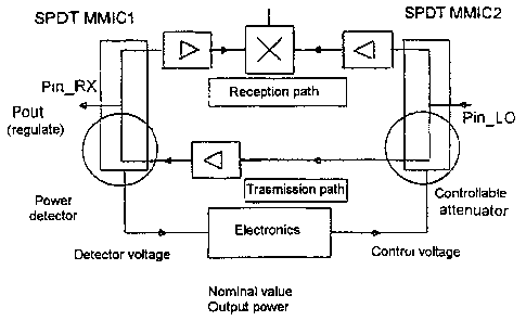
Dans un procédé de régulation de puissance des ondes millimétriques dans le cas d'un module TR bande V, on détecte la puissance de sortie et on la règle à un niveau constant par une électronique de réglage à l'aide d'un atténuateur. Selon l'invention, en mode émission à une fréquence d'au moins 60 GHz, on utilise un premier interrupteur unipolaire à deux directions (SPDT) MMIC comme atténuateur réglable et un deuxième interrupteur SPDT MMIC servant de commutateur émission-réception comme détecteur de puissance de sortie. En mode réception, on utilise les deux interrupteurs SPDT comme commutateurs. Globalement, le réglage de puissance de tout le module TR permet d'augmenter le rendement du module par compensation de la dispersion de la puce et d'obtenir des effets de température. L'utilisation multiple des interrupteurs SPDT MMIC comme commutateurs, atténuateurs et détecteurs de puissance permet de réduire les coûts.


Abrégé anglais


The invention relates to a method for regulating the power of millimetre waves
for a V-band TR module. According to said method, the power output is detected
and regulated at a constant level with a regulating electronics system, by
means of a damping member. The invention provides that for transmission, for
operation at a frequency in the 60 GHz range and higher, a first SPDT (single
pole double throw) MMIC switch is used as a regulated damping member and a
second SPDT MMIC switch which acts as a transmit-receive changeover switch is
used as a power output detector. For reception, both SPDTs are used as
switches. Overall, the power regulation for the entire TR module results in an
increase of the module yield through compensation of chip leakage and
temperature effects. The multiple use of the SPDT MMICs as switches, damping
member and power detector saves costs.

Revendications

Note : Les revendications sont présentées dans la langue officielle dans laquelle elles ont été soumises.


6
WHAT IS CLAIMED IS:
1. Method to control the power of millimetric waves for a V-band TR module at
a
frequency in the range of 50 GHz and higher, the method comprising the acts of
separating the transmission and receiving path via two SPDT (single pole
double
throw) MMIC switches, for the transmission, the first SPDT MMIC switch as a
variable attenuator and the second SPDT MMIC switch as a detector for the
output
power; and by way of an electronic control circuit, the control of the output
power to a
defined level is achieved.
2. Device to control the power of millimetric waves for a V-band TR module at
a
frequency in the range of 50 GHz and higher, comprising: two SPDT (single pole
double throw) MMIC switches for separating the transmit and receive path;
wherein
for transmission, the first SPDT MMIC switch is used as a variable attenuator
and the
second SPDT MMIC switch is used as a detector for the output power, and an
electronic unit to control the output power; wherein in the case of the SPDT
MMIC
having two switch arms, on each switch arm, two parallel-connected diode
pairs,
respectively are connected between the RF line and ground, and wherein, in
operation as a power detector, one arm is blocked and the second arm is
switched
via a bias voltage of 0 V to conducting, and further wherein the RF power
flowing
through the latter arm is rectified at the diodes, and the measurable
rectified voltage
is used as a measurement for the transmitted power.
3. Device to control the power of millimetre waves for a V-band TR module at a
frequency in the range of 50 GHz and higher, comprising: two SPDT (single pole
double throw) MMIC switches for separating the transmit and receive path;
wherein
for transmission, the first SPDT MMIC switch is used as a variable attenuator
and the
second SPDT MMIC switch is used as a detector for the output power; and an
electronic unit to control the output power; wherein in the case of the SPDT
MMIC

7
having two switch arms, in switch mode, an input power at the IN port can
optionally
be switched to the O1 or O2 port, and wherein, in a mode as a variable
attenuator,
the O2 port is terminated in a reflection free manner and a variable
attenuation can
be set between the IN and O1 port by variation of the supply voltage.

Description

Note : Les descriptions sont présentées dans la langue officielle dans laquelle elles ont été soumises.


CA 02430326 2009-01-28
1
METHOD AND DEVICE FOR REGULATING THE POWER OF MILLIMETER
WAVES FOR A V-BAND TR MODULE
The invention relates to a method and a device for regulating the power of
millimetric
waves in a V-band TR module.
Particularly in mobile communications devices, the
output power should be as constant as possible, to be
precise irrespective of individual characteristics of
the components and appliances which are produced in
large quantities. Controllable attenuators are produced
on MMICs with PIN diodes or as MESFET switches for
frequencies below 50 GHz. Other power regulation
concepts for lower frequencies are also known from the
prior art. However, no V-band TR module with a
regulated output power is currently known. Furthermore,
no controllable attenuator for 60 GHz is currently
commercially available as an MMIC.
The individual adjustment of manufactured appliances is
highly costly; it would therefore be desirable to avoid
this by appropriate design. A further aim at the same
time is that as few additional components as possible
should be required since, on the one hand, they
themselves once again have individual scatters and, on
the other hand, result in costs.
The company United Monolithic Semiconductors S.A.S.,
91401 Orsay Cedex France offer a 50-60 GHz SPDT
(= Single Pole Double Throw) switch for communication
systems with the type designation "CHS2190a", which has

CA 02430326 2009-01-28
2
already been used as a transmission/reception
changeover switch in transmission/reception modules.
The aim of the invention is to use this or a
corresponding switch to provide power regulation with
said features.
According to one aspect of the invention, there is provided a method to
control the
power of millimetric waves for a V-band TR module at a frequency in the range
of 50
GHz and higher, the method comprising the acts of: separating the transmission
and
receiving path via two SPDT (single pole double throw) MMIC switches, for the
transmission, the first SPDT MMIC switch as a variable attenuator and the
second
SPDT MMIC switch as a detector for the output power; and by way of an
electronic
control circuit, the control of the output power to a defined level is
achieved.
Another aspect of the invention concerns a device to control the power of
millimetric
waves for a V-band TR module at a frequency in the range of 50 GHz and higher,
comprising: two SPDT (single pole double throw) MMIC switches for separating
the
transmit and receive path; wherein for transmission, the first SPDT MMIC
switch is
used as a variable attenuator and the second SPDT MMIC switch is used as a
detector for the output power, and an electronic unit to control the output
power;
wherein in the case of the SPDT MMIC having two switch arms, on each switch
arm,
two parallel-connected diode pairs, respectively are connected between the RF
line
and ground, and wherein, in operation as a power detector, one arm is blocked
and
the second arm is switched via a bias voltage of 0 V to conducting, and
further
wherein the RF power flowing through the latter arm is rectified at the
diodes, and the
measurable rectified voltage is used as a measurement for the transmitted
power.
Yet another aspect of the invention concerns a device to control the power of
millimetre waves for a V-band TR module at a frequency in the range of 50 GHz
and
higher, comprising: two SPDT (single pole double throw) MMIC switches for
separating the transmit and receive path; wherein for transmission, the first
SPDT

CA 02430326 2009-01-28
2a
MMIC switch is used as a variable attenuator and the second SPDT MMIC switch
is
used as a detector for the output power; and an electronic unit to control the
output
power; wherein in the case of the SPDT MMIC having two switch arms, in switch
mode, an input power at the IN port can optionally be switched to the 01 or 02
port,
and wherein, in a mode as a variable attenuator, the 02 port is terminated in
a
reflection free manner and a variable attenuation can be set between the IN
and 01
port by variation of the supply voltage.
The use of a SPDT MMIC as a controllable attenuator
makes it possible to set a desired transmission power
and to compensate for scatters between the chips. This
forms the core component for power regulation (control
element). The double function of the chip results in
considerable cost savings.
The use of the second SPDT MMIC as a power detector
also results in costs being saved, owing to the double
function.
Overall, the power regulation for the entire TR module
leads to an increase in the module yield by
compensation for scatters between chips and temperature
effects. The multiple use of the SPDT MMICs as
switches, as an attenuator and as a power detector
leads to the stated advantages.
Details of the invention can be found in the dependent
claims and in the description, in which one exemplary
embodiment is described with reference to the drawing,
in which:

CA 02430326 2009-01-28
2b
Figure 1 shows a block diagram of the transmission
power regulation according to the invention,
Figure 2 shows the layout and the pad designations for
the known SPDT MMIC,
Figure 3 shows the outline circuit diagram,
Figure 4 shows the external circuitry and the DC
supply,

CA 02430326 2003-05-28
WO 02/47245 - 3 - PCT/DE01/04215
Figure 5 shows the attenuation response as a function
of the monitor voltage,
Figure 6 shows the use of the SPDT MMIC as a detector,
and
Figure 7 shows the maximum available and regulated
transmission power.
According to the invention, the known MMIC may be
operated either as a Schottky diode switch of the SPDT
(Single Pole Double Throw) type or, by different supply
voltages, as a controllable attenuator. Figures 2 and 3
show the layout of the SPDT MMIC and an outline circuit
diagram. During switching operation, the input power of
the port IN is passed on either to the port 01 or 02.
For operation as a variable attenuator, the port 02 is
terminated without any reflection, and the switching
arm IN-02 is operated in the forward-biased direction.
A variable attenuation of between 3.5 and 25 dB can be
produced between the ports IN and 01, via the DC supply
voltage (see Figures 4 and 5).
Figure 4 shows the external circuitry and a DC supply.
The operating modes are as follows:
Switching operation:
Switching arm IN-01 in the ON state, switching arm IN-
02 in the OFF state:
Pads A1,A2: -2.5 V
Pads B1,B2: 12 mA
OFF-state: switching arm switched off
ON-state: switching arm switched on
The external supply voltage is provided via series
resistors of about 250 ohms in series with the pads
Al, A2, Bl, B2.

CA 02430326 2003-05-28
WO 02/47245 - 4 - PCT/DE01/04215
Detector operation:
Switching arm IN-O1 as a detector, switching arm IN-02
in the OFF state:
Pads A1,A2: 0 V, (1 kohm in series with pads)
Pads B1,B2: 12 mA
Operation as a variable attenuator:
Switching arm IN-Ol in the ON state (port 01 terminated
without any reflections),
Switching arm IN-02 in the attenuation mode:
Pads A1,A2: -2.5 V
Pads B1,B2: 0-12 mA (corresponds to 0-4 V across
the series resistance of 250 ohms)
Two diode pads 4/5 and 6/7 are connected between the RF
line and ground on each switching arm on the SPDT MMIC.
When the SPDT MMIC is being operated as a power
detector, one arm is switched off (for example IN-02),
while the second arm is switched on with a bias voltage
of 0 V. The RF power flowing through the ON arm is
rectified by the parallel-connected diodes. The control
voltage which can be measured on the pads Al and A2 is
a measure of the power flowing through, as is shown in
Figure 6. The control voltage on the pad A2 is used for
the power measurement. An SPDT MMIC can be used for
power detection for levels of 3 dBM<P<10 dBm.
Figure 5 shows the attenuation response as a function
of the monitor voltage. In this case, the values are as
follows:
DC circuitry and voltage supply:
Pads A1,A2: -2.5 V
Pads B1,B2: monitor voltage applied across a
250 ohm series resistance.

CA 02430326 2003-05-28
WO 02/47245 - 5 - PCT/DE01/04215
RF configuration
Measurement on the wafer sample at 58 GHz
Input power at the port IN, output power at the port
02, port 01 was terminated by a 10 dB attenuator.
Figure 6 shows the use of the SPDT MMIC as a detector.
The diagram shows the detector voltage as a function of
the measured output power. In this case:
DC circuitry and voltage supply:
Pads Al, A2: 0 V supplied via a 1 kohm series
resistance
Pads B1,B2: 12 mA
RF configuration:
Measurement on wafer sample at 58 GHz
Input power at the port 01, output power at the port
IN, port 02 was terminated with a 10 dB attenuator
The transmission power regulation according to the
invention was developed using the described components
for a transmission/reception module, as is shown in
simplified form in the block diagram in Figure 1.
During reception, both SPDT MMICs (1 and 2) are used as
switches. The LO power (Pin_LO) and the reception power
(Pin_RX) are passed to the mixer. During transmission,
the SPDT MMIC 1 acts as a controllable attenuator, and
SPDT MMIC 2 acts as a power detector. The power control
loop is closed via analog electronics. The desired
output value is set on the electronics via the nominal
value.
Figure 7 shows the output power measured at the
spectrum analyzer for the unregulated case (maximum
available power) and for the regulated case
(Pout=5dBm=const).

Dessin représentatif
Une figure unique qui représente un dessin illustrant l'invention.
États administratifs

2024-08-01 : Dans le cadre de la transition vers les Brevets de nouvelle génération (BNG), la base de données sur les brevets canadiens (BDBC) contient désormais un Historique d'événement plus détaillé, qui reproduit le Journal des événements de notre nouvelle solution interne.

Veuillez noter que les événements débutant par « Inactive : » se réfèrent à des événements qui ne sont plus utilisés dans notre nouvelle solution interne.

Pour une meilleure compréhension de l'état de la demande ou brevet qui figure sur cette page, la rubrique Mise en garde , et les descriptions de Brevet , Historique d'événement , Taxes périodiques et Historique des paiements devraient être consultées.

Historique d'événement

Description Date
Le délai pour l'annulation est expiré 2012-11-09
Lettre envoyée 2011-11-09
Inactive : Correspondance - TME 2010-08-10
Accordé par délivrance 2009-07-28
Inactive : Page couverture publiée 2009-07-27
Inactive : Taxe finale reçue 2009-05-11
Préoctroi 2009-05-11
Un avis d'acceptation est envoyé 2009-04-06
Lettre envoyée 2009-04-06
Un avis d'acceptation est envoyé 2009-04-06
Inactive : Approuvée aux fins d'acceptation (AFA) 2009-04-03
Modification reçue - modification volontaire 2009-01-28
Inactive : Dem. de l'examinateur par.30(2) Règles 2008-07-31
Lettre envoyée 2004-09-21
Exigences pour une requête d'examen - jugée conforme 2004-09-02
Toutes les exigences pour l'examen - jugée conforme 2004-09-02
Requête d'examen reçue 2004-09-02
Inactive : IPRP reçu 2003-09-22
Inactive : Page couverture publiée 2003-07-29
Inactive : Notice - Entrée phase nat. - Pas de RE 2003-07-24
Lettre envoyée 2003-07-24
Demande reçue - PCT 2003-07-03
Exigences pour l'entrée dans la phase nationale - jugée conforme 2003-05-28
Demande publiée (accessible au public) 2002-06-13

Historique d'abandonnement

Il n'y a pas d'historique d'abandonnement

Taxes périodiques

Le dernier paiement a été reçu le 2008-10-23

Avis : Si le paiement en totalité n'a pas été reçu au plus tard à la date indiquée, une taxe supplémentaire peut être imposée, soit une des taxes suivantes :

  • taxe de rétablissement ;
  • taxe pour paiement en souffrance ; ou
  • taxe additionnelle pour le renversement d'une péremption réputée.

Les taxes sur les brevets sont ajustées au 1er janvier de chaque année. Les montants ci-dessus sont les montants actuels s'ils sont reçus au plus tard le 31 décembre de l'année en cours.
Veuillez vous référer à la page web des taxes sur les brevets de l'OPIC pour voir tous les montants actuels des taxes.

Historique des taxes

Type de taxes Anniversaire Échéance Date payée
Enregistrement d'un document 2003-05-28
Taxe nationale de base - générale 2003-05-28
TM (demande, 2e anniv.) - générale 02 2003-11-10 2003-10-28
Requête d'examen - générale 2004-09-02
TM (demande, 3e anniv.) - générale 03 2004-11-09 2004-10-27
TM (demande, 4e anniv.) - générale 04 2005-11-09 2005-10-24
TM (demande, 5e anniv.) - générale 05 2006-11-09 2006-10-25
TM (demande, 6e anniv.) - générale 06 2007-11-09 2007-10-24
TM (demande, 7e anniv.) - générale 07 2008-11-10 2008-10-23
Taxe finale - générale 2009-05-11
TM (brevet, 8e anniv.) - générale 2009-11-09 2009-10-30
TM (brevet, 9e anniv.) - générale 2010-11-09 2010-10-28
Titulaires au dossier

Les titulaires actuels et antérieures au dossier sont affichés en ordre alphabétique.

Titulaires actuels au dossier
EADS DEUTSCHLAND GMBH
Titulaires antérieures au dossier
JOERG SCHROTH
MARION FILLEBOCK
Les propriétaires antérieurs qui ne figurent pas dans la liste des « Propriétaires au dossier » apparaîtront dans d'autres documents au dossier.
Documents

Pour visionner les fichiers sélectionnés, entrer le code reCAPTCHA :


Pour visualiser une image, cliquer sur un lien dans la colonne description du document. Pour télécharger l'image (les images), cliquer l'une ou plusieurs cases à cocher dans la première colonne et ensuite cliquer sur le bouton "Télécharger sélection en format PDF (archive Zip)" ou le bouton "Télécharger sélection (en un fichier PDF fusionné)".

Liste des documents de brevet publiés et non publiés sur la BDBC .

Si vous avez des difficultés à accéder au contenu, veuillez communiquer avec le Centre de services à la clientèle au 1-866-997-1936, ou envoyer un courriel au Centre de service à la clientèle de l'OPIC.


Description du
Document 
Date
(aaaa-mm-jj) 
Nombre de pages   Taille de l'image (Ko) 
Description 2003-05-27 5 196
Dessins 2003-05-27 4 91
Abrégé 2003-05-27 2 93
Revendications 2003-05-27 2 61
Dessin représentatif 2003-07-27 1 10
Description 2009-01-27 7 248
Revendications 2009-01-27 2 54
Dessin représentatif 2009-07-05 1 12
Rappel de taxe de maintien due 2003-07-23 1 106
Avis d'entree dans la phase nationale 2003-07-23 1 189
Courtoisie - Certificat d'enregistrement (document(s) connexe(s)) 2003-07-23 1 106
Accusé de réception de la requête d'examen 2004-09-20 1 185
Avis du commissaire - Demande jugée acceptable 2009-04-05 1 163
Avis concernant la taxe de maintien 2011-12-20 1 171
PCT 2003-05-27 5 174
PCT 2003-05-28 2 67
Correspondance 2009-05-10 2 54
Correspondance 2010-08-09 1 47
Correspondance 2011-12-20 1 65