Note: Descriptions are shown in the official language in which they were submitted.
CA 02431064 2003-06-12
WO 02/054505 PCT/GBO1/05715
1
SYSTEM AND METHOD FOR EI~ECTRICAI~LY INDUCED
BREAKDOWN OF NANOSTRUCTURES
BACKGROUND OF THE INVENTION
Field of the Invention
The present invention relates to nanostructures, and more
particularly to a system and method of electrically induced breakdown of
nanostructures.
Description of Related Art
In the field of molecular nanoelectronics, few materials show as
much promise as nanotubes, and in particular carbon nanotubes, which
comprise hollow cylinders of graphite, angstroms in diameter. Nanotubes
can be made into tiny electronic devices such as diodes and transistors,
depending on the nanotube's electrical characteristics. Nanotubes are
unique for their size, shape, and physical properties. Structurally a
carbon nanotube resembles a hexagonal lattice of carbon rolled into a
cylinder.
Besides exhibiting intriguing quantum behaviors at low temperature,
carbon nanotubes exhibit at least two important characteristics: a
nanotube can be either metallic or semiconductor depending on its
chirality (i.e., conformational geometry). Metallic nanotubes can carry
extremely large current densities with constant resistivity.
Semiconducting nanotubes can be electrically switched on and off as
field-effect transistors (FETs). The two types may be covalently joined
(sharing electrons). These characteristics point to nanotubes as excellent
materials for making nanometer-sized semiconductor circuits.
Current methods of studying nanotubes rely on the random formation
of both metallic and semiconducting nanotubes. There is no known method
for reliably preparing a nanotube having particular characteristics, much
less for preparing nanotubes to exhibit functional behavior such as
transistors, diodes, etc. Nor are there known methods of nanotube
separation by selective synthesis or post-synthesis which have proven to
have any measurable level of success. Heretofore, nanotubes must have
either been individually separated from mixtures of metallic and
semiconducting nanotubes or randomly placed over an electrode to be
studied. However, there is no observable consistency in such methods.
CA 02431064 2003-06-12
WO 02/054505 PCT/GBO1/05715
2
This lack of control, compounded by nanotubes' tendency to bundle
together, has hindered the study of nanotube physics and is seen as a
primary roadblock in the nanotube development including nanotube-based
electronic technology. Therefore, a need exists for a system and method of
preparing nanotubes having desired characteristics.
SUMMARY OF THE INVENTION
Accordingly, the invention provides a method for forming a device
comprising the steps of, providing a substrate, providing a plurality of
nanotubes in contact with the substrate, and selectively breaking a
nanotube using an electrical current. Preferably the method further
comprises the step of depleting a semiconducting nanotube of carriers
using an electric current.
Preferably depleting a semiconducting nanotube of a plurality of
carriers further comprises the step of applying a voltage to a gate
electrode on the substrate. Preferably the method comprises the step of
applying the electrical current through the nanotube from a source
electrode to a drain electrode.
Preferably, the plurality of nanotubes are multi-walled nanotubes
including metallic and semiconducting nanotubes. Preferably the method
comprises the steps of selectively breaking includes breaking an outer
metallic nanotube.
Preferably the plurality of nanotubes are single-walled nanotube
ropes including metallic and semiconducting nanotubes, wherein the step of
breaking includes breaking at least one metallic nanotube.
Preferably the nanotubes are provided at a density between a
monolayer and about 1/lOth of one percent coverage.
Preferably the substrate is an insulator and includes an arxay of
metallic pads.
Preferably the substrate is silica based and includes the array of
metallic pads.
Preferably each pad includes one of a source electrode, a drain
electrode, and a gate electrode.
CA 02431064 2003-06-12
WO 02/054505 PCT/GBO1/05715
3
Preferably providing a substrate is accomplished using lithography
to form an array of pads, each pad including a corresponding electrode, on
an insulating substrate.
Preferably the nanotubes are carbon nanotubes.
Preferably the method further comprises the step of breaking a
plurality of stray nanotubes.
2O According to another aspect, the invention provides a method of
modifying at least one characteristic of a nanotube, comprising the steps
of providing a mixture of nanotubes, and applying a current to the
mixture, inducing the selective breakdown of the nanotube mixture.
Preferably the method further comprises removing carriers from a
semiconducting nanotube.
Preferably the current selectively breaks metallic nanotubes.
Preferably the power applied to the mixture is about 500: W.
Preferably the nanotube is one of a multi-walled nanotube and a
single-walled nanotube rope.
Preferably the characteristic is one of diameter, density, and
conductance.
Preferably the mixture comprises metallic and semiconducting
nanotubes.
Preferably the current density is greater than 109 A/cm2.
According to another aspect, the present invention provides a method
for forming a device providing an insulating substrate comprising a source
electrode, a drain electrode, and a gate electrode, providing carbon
nanotube bundles including metallic and semiconducting component nanotubes
in contact with the substrate, wherein the nanotubes are provided at a
density of about one percent coverage, further comprising applying a
voltage to the gate electrode to deplete the semiconducting component
nanotubes of carriers, applying an electrical current through the
nanotube, from a source electrode to a drain electrode, and breaks at
0 least one metallic component nanotube to form a field effect transistor.
CA 02431064 2003-06-12
WO 02/054505 PCT/GBO1/05715
4
Preferably the carbon nanotube bundle can be a mufti-walled nanotube
or a single-walled nanotube rope.
BRIEF DESCRIPTION OF THE DRAWINGS
Preferred embodiments of the present invention will be described
below in more detail, with reference to the accompanying drawings:
Figs. la, 1b, and 1c are diagrams of a nanotube and constituent
hexagonal rings;
Fig. 2a is a diagram showing a mufti-walled nanotube;
Fig. 2b is a diagram showing a single-walled nanotube rope;
Fig. 3 is a graph of the partial electrical breakdown of a
mufti-walled nanotube at constant voltage over time;
Fig. 4a is a graph showing the low bias conductance alternatives
between semiconducting and metallic behaviors due to the charging nature
of the outermost shell of a mufti-walled nanotube at each stage of
breakdown;
Fig. 4b is a graph showing the conductance of the remaining
semiconducting shells after the last metallic shell has been removed from
a mufti-walled nanotube;
Fig. 4c is a table showing the relationship between shell number,
diameter, and the relative band gap energy;
Fig. 5 is a graph showing the current (I) versus voltage for each
shell of a mufti-walled nanotube;
Figs. 6a, 6b, 6c, 6d show several conversions of random mixtures of
molecular conductors (nanotubes) into semiconducting field effect
transistors;
Fig. 7a is a diagram showing an array of electrodes; and
Fig. 7b is a diagram of a single-walled nanotube rope based field
effect transistor including a source, drain, and gate.
DETAILED DESCRIPTION OF PREFERRED EMBODIMENTS
According to the present invention a method of permanently modifying
a mufti- walled nanotube (MWNT) or a single-walled nanotube (SWNT) rope or
bundle is provided. A nanotube can be metallic or semiconductor depending
on its chirality (i.e., conformational geometry). Both species are found
in MWNTs and SWNTs. A method according to the present invention uses
current-induced electrical breakdown to eliminate individual nanotubes
having a particular characteristic. The method is able to tailor the
properties of a composite nanotube by changing the proportion of component
CA 02431064 2003-06-12
WO 02/054505 PCT/GBO1/05715
nanotubes. It should be noted that while the present invention is
described using carbon based nanotubes, the illustrative methods are
applicable to any molecular structure in which a current can be applied
selectively to particular surface areas. For example, the present
5 invention can also be used in Boron-Nitride (BN) and metal dichalcogenids
(MXz) based nanostructures.
Carbon nanotubes can withstand current densities exceeding 109 A/cmz,
in part due to the strength of carbon-to-carbon bonds (e. g., the bond
strength for a single C-C bond is about 347 kJ/mol). Ultimately however,
at high enough currents, nanotubes will fail. For example, for a MWNT,
failure occurs in air at a certain threshold power, e.g., approximately
500:W, above which the rapid oxidation of the outermost carbon shell is
initiated. Power is equal to current times the potential difference
l5 (i.e., voltage). Because heat induced oxidation of defect-free graphite
only proceeds at extremely high temperatures, e.g., >2000NC, the primary
factor in the breakdown initiation according to the present invention is
current-induced defect formation, with self-heating being a secondary
effect.
Referring to Fig. la, a nanotube 102 includes a hexagonal lattice of
carbon or other molecules. In the case of carbon, a ring 104 can be built
including six carbons covalently bonded to one another. Fig. 1b shows an
individual carbon ring, each intersection 106 indicates an individual
carbon atom, bonds are also indicated as 107. An alternative structure is
a boron-nitride ring, one form is shown in Fig. lc. The boron-nitride ring
may includes three boron atoms, e.g., 110, bonded to three nitrogen atoms,
e.g., 108, in an alternating pattern.
By taking advantage of the current-induced defect formation, a
method according to the present invention selectively breaks
current-carrying nanotubes without affecting parallel nanotubes in cases
where the parallel nanotubes carry little or no current. For example,
MWNTs as shown in Fig. 2a, favor the outermost shell 102 because it is in
direct contact with external electrodes (e. g., a source and a drain). This
distribution can leave the innermost shells carrying little or no current,
which protects them during current-induced oxidation. In a SWNT rope,
shown in Fig. 2b, individual nanotubes (e.g., 102) are arranged in
parallel. The distribution of current through a SWNT rope is more uniform
than through a MWNT because the individual nanotubes of a SWNT rope can be
simultaneously in good contact with the external electrodes.
CA 02431064 2003-06-12
WO 02/054505 PCT/GBO1/05715
6
Generally there is no reason for a current to favor some SWNTs over
others, however, according to an embodiment of the present invention, an
electrostatically coupled gate electrode can selectively deplete the
component semiconducting nanotubes of their carriers. In other words, for
a SWNT or MWNT which spans a source electrode and a drain electrode, by
applying a voltage to a corresponding gate electrode, carriers can be
depleted from the component semiconducting nanotubes. Once depleted, the
semiconducting nanotubes are protected from damage, and high current
densities applied to the SWNT or MWNT by the source electrode can be used
to initiate oxidation of the component metallic nanotubes. Thus, these
methods can protect semiconducting nanotubes within a SWNT rope as well as
an outer semiconducting MWNT shell. The removal of carbon nanotubes from
these composite conductors can be observed both electrically and through
microscopy. Electrically, the breakdown of a single carbon nanotube
results in a partial conductance drop, typically completed in a few
milliseconds. When stressed at sufficiently high bias, multiple
independent drops occur as one carbon shell after another is broken. The
electronics used in the breakdown are capable of controlling the number of
nanotubes broken. Upon sensing a drop in current, e.g., about 19 :A, the
electronics are able to stop the breakdown process, thereby controlling
the exhibited characteristics.
Referring to Fig. 3, the partial electrical breakdown of a MWNT at
constant voltage stress proceeds in a series of discrete steps
corresponding to the loss of eight individual layers of the MWNT. These
results were obtained at a power of about 450:W, and a potential difference of
about 2
volts. The regular breakdown in current of about 19:A per shell can also be
seen in Fig. 3. A decrease in radius of a partially broken MWNT is equal
to the intershell spacing (0.34nm) times the number of completed breakdown
steps. A similar thinning can be accomplished with a SWNT bundle with
metallic SWNTs being selectively broken leaving only the semiconducting
SWNTs.
The breakdown is aided by the sensitivity of nanotubes to external
stresses, since relatively small electric fields and currents can affect
individual molecules. For example, a semiconducting nanotube 1nm in
diameter can be electrostatically depleted of electrical carriers by a
gate electrode hundreds of manometers away. The current density
(sufficient to affect nanotube breakdown) acts as a catalyst, initiating a
chemical reaction between the nanotube and surrounding gasses. For
example, for a carbon nanotube in air, the reaction can be written as: C
(nanotube) + 02 (gas) -~ COz (gas) .
CA 02431064 2003-06-12
WO 02/054505 PCT/GBO1/05715
7
The present invention also contemplates other environments, wherein
nondestructive current-assisted reactions can chemically modify particular
nanotubes. The resulting devices could incorporate both electrical
switching and chemical sensitivity. For example, using a nanotube's
sensitivity to various gases, chemical modification can be used in the
context of a chemical nanosensor, where a change in the conductivity of a
nanosensor (nanotube) signals the presence of a particular gas.
The controlled destruction of nanotubes allows for the separation of
semiconducting SWNTs from mixtures of SWNTs (including metallic and
semiconducting SWNTs) and the preparation of nanotube-based field effect
transistors (FETs). It should also be noted that, the methods disclosed
herein can be used to prepare transistors (e.g., a FET), diodes, and
resistors, depending on the characteristics of the nanotubes and the
design of the substrate.
Fundamentally, the process can facilitate the study of the complex
electronic structures and transport properties of MWNTs and SWNT ropes. By
removing the stress (current) at the occurrence of individual conductance
steps, these composite nanowires may be re-characterized upon the loss of
each constituent conductor (nanotube). Characterization refers to, for
example, the conductance properties of a MWNT or SWNT rope from one stage
in the breakdown process to another. Multiple complementary transport
measurements can, for example, probe deeper and deeper into the inner
shells of a MWNT, allowing for the characterization, as well as a direct
comparison, of transports through each shell.
The different shells of a MWNT are presumed to alternate in a random
fashion between metallic and semiconducting. This can be directly tested
by using controlled breakdown followed by low bias or low temperature
measurements, which probe the outermost shell of a MWNT. Following
previous measurements on SWNTs, the semiconducting and metallic shells can
be differentiated by measuring the conductance G as a function of gate
voltage Vg using a relatively small, lOmV source-drain bias. A metallic
shell is characterized by a G which is independent of Vg, or nearly so,
whereas a semiconducting shell can be electrostatically depleted of
carriers by the gate.
Referring to Fig. 4a, by halting the stress upon each breakdown
event, a MWNT may be characterized after the loss of each constituent
shell. Fig. 4a shows the low bias conductance (G(Vg)) alternates between
CA 02431064 2003-06-12
WO 02/054505 PCT/GBO1/05715
8
semiconducting (e.g., 402 and 406) and metallic (e.g., 404) behaviors due
to the changing nature of the outermost shell at each stage of breakdown.
In Fig. 4b, when the last metallic shell (n-9) has been removed, the
remaining semiconducting shells can be completely depleted to give regions
of zero conductance. Taking the indicated peaks in G(Vg) to correspond to
conductance and valence band edges, the band gaps of different shells can
be determined within a constant or proportionality. The relative widths
agree with calculations based on the expected diameter dependence as shown
in Fig. 4c, in which the only parameters are the initial diameter of the
tube and the 0.34nm spacing between adjacent shells.
Fig. 4a shows the room temperature G(Vg) for various different
layers within a MWNT. Initially, the MWNT has a diameter of 9.5nm, n
shells, and a metallic G(Vg). Fig. 4a shows the strong modulation in G(Vg)
observed after removing three shells 402. Removing a fourth layer results
in a metallic G(Vg) 404, and removing the sixth shell produces another
semiconducting G(Vg) 406. This variation is interpreted as a signature of
the alternating character of the carbon shells being removed.
The fact that G does not fall to zero for a particular
semiconducting shell is due to the contribution of inner metallic shells
which continue to conduct. Shells n-3 and n-4 demonstrate this: the
depletion minimum of the G(Vg) curve for shell n-3 coincides with the
conductance of the underlying shell n-4 408. In this case, the outer,
semiconducting shell n-3 can be fully depleted by the gate, but the
measured conductance includes leakage through the underlying metallic
shell. Additional measurements show that this leakage is energetically
frozen out in the low temperature, the low bias limit indicating that the
intershell coupling is thermally activated. The gradual thinning of MWNTs
and SWNT ropes can be resolved using, for example, atomic force and
scanning electron microscopy with a linear correspondence between the
number of breakdown steps and change in apparent diameter.
Upon removing the tenth carbon shell, the MWNT begins to behave like
a perfect, intrinsic field-effect transistor (FET), with a region of zero
conductance even at room temperature due to the complete depletion of
carriers (e. g., Fig. 4b). Similar characteristics are found for individual
semiconducting SWNTs, though the SWNTs used were strongly p-type and did
not have symmetric G(Vg) characteristics. The complete depletion of the
MWNT indicates that no metallic shells remain, and this behavior persists
until the fourteenth carbon shell is removed, at which time the MWNT
circuit opens. Based on the known intershell spacing of nearly 0.34nm, a
CA 02431064 2003-06-12
WO 02/054505 PCT/GBO1/05715
9
MWNT of this diameter can have at most fourteen shells, in agreement with
the shell-by-shell count.
Fig. 4b shows the gradual increase of the zero conductance region as
the final semiconducting shells are removed. The width of this region is
proportional to the band gap (the energy needed to break a bond) of the
semiconductors, with conduction above and below the gap due to
electron-like and hole-like carriers, respectively. Due to the use of high
voltage pulses to break shells, some rearrangement of trapped charges
occurs on an underlying SiOz substrate. To simplify the comparison among
shells, the curve shown in Fig. 4b is centered near Vg=0. A characteristic
of semiconducting carbon nanotubes is that the band gap energy is
inversely proportional to diameter, so that progressively smaller carbon
shells exhibit larger band gaps, the width of the band gap determining the
type of material (conductor, semiconductor, insulator). Using only the
initial MWNT diameter and the intershell spacing, the expected ratios
between band gap of the innermost shells can be calculated. As shown in
Fig. 4c, these ratios agree with the experimental ratios, as defined by
the conductance peaks on either side of the conductance gap and indicated
in Fig. 4c.
Referring now to Fig. 5, by recharacterizing the MwNT after the loss
of individual shells, the contribution of each shell to the I-V can be
determined. Based on the uniform spacing of the sequence of I-VS, each
shell saturates at the same current, and that all shells contribute to
conduction at moderate and high bias. The dashed line indicates the
position of an I-V which was not acquired. A semilog plot of selected I-Vs
indicates a tendency towards exponential I-Vs for the innermost shells due
to the effective barrier between them and the external electrodes. Similar
barriers likely play a role in all shells except the outermost one, and
explain the nonlinearities observed in some MWNTs but not others.
Fig. 5 shows a sequence of high bias current-voltage characteristics
(I-Vs), effectively re-characterizing the MWNT with n, n-1, n-2; etc.
shells, until only a single shell remains. High bias I-Vs must be acquired
in high vacuum, e.g., < lmillibar or in an inert environment, to suppress
destructive oxidation. Between each curve, the MWNT was exposed to air in
order to controllably remove single carbon shells. Four-probe and
two-probe measurements were periodically compared to monitor the contact
resistance (Rc) to each nanotube. The data shown here are for samples
exhibiting constant Rc of a few kOhms throughout the series of
measurements. Samples with high Rc tend to fail at the contact, as opposed
CA 02431064 2003-06-12
WO 02/054505 PCT/GBO1/05715
to the shell-by-shell mechanism described herein. Each I-V shows current
saturation at a steadily increasing bias, similar to that observed in
individual SWNTs, but at much higher currents. The removal of each shell
from the MWNT appears to decrease this saturation level by a fixed amount
5 of approximately 20uA, in agreement with Fig. 3. This step-by-step
decrease clearly indicates a high bias, that all of the MWNT shells
contribute to transport and saturate equally.
Besides the decrease of the current saturation value, the sequence
10 of I-Vs in Fig. 5 also exhibits increasing nonlinearity as shells are
removed. A semilog plot of selected I- Vs shows the trend from a linear
I-V towards an exponential characteristic of the form I = A exp(V/Vo), with
Vo = 0.50V. Apparently, a tunneling barrier dominates the I-V of the
innermost shells, most likely because these shells can only couple to the
external electrodes through a barrier composed of many graphitic layers.
For intermediate shells, not in direct contact with the electrodes, the
unusual shape of the measured I-Vs can be understood qualitatively as due
to a depth-dependent barrier in series with a nanotube's intrinsic,
longitudinal I-V characteristic. This series barrier explains the gradual
increase of the bias required to reach current saturation shown in Fig. 5.
Furthermore, the transition from linear to nonlinear I-Vs observed here,
and the abundance of similar nonlinear I-Vs reported in the literature
suggests that transport experiments often do not directly contact the
current-carrying carbon shell of a MWNT, but rather contact the partial or
incomplete shells typically observed by transmission electron microscopy.
Figs. 4a, 4b, 4c and 5 confirm the varying nature of MWNT shells,
quantitatively address the coupling between these shells, and attempt to
isolate the contribution of a single shell to the overall conductance.
Until now, theory and experiment have been divided over these issues. On
one hand, MWNTs are too complex to realistically model theoretically, and
on the other hand no experiments have been able to directly probe the
inner carbon. shells. The powerful technique of controlled breakdown
introduced here has the potential to provide new insights into the
transport properties of these complex conductors. In addition, a MWNT can
be selectively converted between metal and semiconductors with different
band gaps.
The methods described for MWNTs can be applied to SWNT ropes.
Although both MWNTs and SWNTs are composite nanotubes, SWNTs exhibit some
differences. For example, multiple SWNTs within a rope can be in contact
with their potentially oxidizing environment, allowing the simultaneous
CA 02431064 2003-06-12
WO 02/054505 PCT/GBO1/05715
11
failure of many carbon shells rather than the uniform, shell-by-shell
failure observed in a MWNT (e.g., Fig. 3). In addition, the SWNTs within a
rope do not electrostatically shield each other as effectively as the
shells of a MWNT. As a result, the breakdown in a rope can be directed
solely at the metallic SWNTs by depleting the semiconducting SWNTs of
carriers (in this case, Vg is held at +10V during the stress to deplete
the predominantly p-type SWNTS of carriers). Carrier densities in carbon
based SWNTS can range from about 100 to about 1000 electrons/:m. Another
difference is that each SWNT in a small rope connects independently to the
external electrodes. Thus, more so than for a MWNT, a rope may be modeled
as independent, parallel conductors with total conductance G(Vg) = Gm +
Gg(Vg), where Gm is the contribution of the metallic nanotubes and Gg is
the gate-dependent conductance of the semiconducting nanotubes.
Referring to Figs. 6a and 6b, by stressing a SWNT rope including a
mixture of semiconducting and metallic SWNTs while simultaneously gating
the bundle, the semiconductors are depleted of carriers in the selective
breakdown of the metallic SWNTs. The initial SWNT bundles 602 and 606
include both metallic and semiconducting SWNTS, while the thinned SWNT
bundles 604 and 608 include far higher proportions of semiconducting
SWNTs. Likewise, semiconducting nanotube shells of MWNTs can be
effectively insulated be depleting the shells of carriers using similar
methods as those for SWNTs. Thus the breakdown of a MWNT can be controlled
to yield desired characteristics (e.g., metallic or semiconducting). The
selective breakdown of a composite nanotube can be explained by the
relative dependencies of metallic and semiconducting nanotubes on a gate
voltage. The conductance of metallic nanotubes show little dependence on
gate voltages, however, the conductance of semiconducting nanotubes
exhibit a strong dependence on gate voltage.
Thus, as shown in Figs. 6a and 6b, at positive gate voltages, the
conductance of the SWNT approaches zero, while at negative gate voltages,
the conductance increases as carriers are added. Figs. 6a and 6b depict
G(Vg) for two small SWNT ropes before and after controlled breakdown
respectively. The unperturbed samples have a conductance which can be
partially modulated by the gate electrode, much like the case for MWNTs.
As the metallic SWNTs in the rope are destroyed, the underlying
conductance Gm decreases to zero. In contrast, the extent of modulation Ge
does not change. The measurements indicate that, by depleting the
semiconducting SWNTs of carriers during the breakdown process, they can be
effectively protected from damage. This result suggests little electronic
interaction between different SWNTs in a rope. Measurements of changes in
CA 02431064 2003-06-12
WO 02/054505 PCT/GBO1/05715
12
the temperature dependence of G(Vg) could address the issue of
interactions and determine at what energy range, if any, such interactions
becomes important.
With the semiconducting SWNTs unaffected, the G(Vg) curve is rigidly
shifted downwards according to the contribution of the metallic SWNTS.
Referring to Fig. 6c, even for very large ropes containing hundreds of
SWNTS, these samples can be effectively converted into FETs. However, in
this case the gradual decrease of Gm halts before it reaches zero,
presumably because metallic SWNTs at the core of the rope are encased by
semiconducting SWNTS. The ultimate destruction of these weakly-coupled
metallic SWNTs can require higher voltages and may sacrifice some
surrounding semiconducting SWNTs. As a result, a rope with many
semiconducting channels and a large, initial modulation GH >l0us may only
result in a FET with Ga ~ lus.
Besides being useful for the study of MWNTs and SWNT interactions,
the controlled breakdown technique is extremely valuable for the
fabrication of nanotube- based electronic devices. Until now, SWNT FETs
have been fabricated individually. Typically, very low surface coverage
has ensured that at most one SWNT connects a source and drain electrode at
this density, most prospective circuits remain disconnected but some
incorporate a metallic SWNT while others have a semiconducting SWNT.
While this technique has proven valuable for the initial
characterization of SWNT properties, practical applications will need
reliable generation of many devices in parallel. Achieving densely packed
FETs, for example, needs purely semiconducting SWNTs at a sufficient
density to interconnect all of the desired positions. The nanotubes may
be provided by known techniques, such as, in-situ growth by chemical vapor
deposition or grown ex-situ and deposited. High surface densities favor
multiple SWNTs and SWNT ropes, which due to the variability of SWNT
properties, are dominated by metallic tubes, useless as semiconducting
channels. At present, no method is known to exist for the synthesis of
purely semiconducting SWNTs or for the separation of semiconducting SWNTs
from SWNT mixtures.
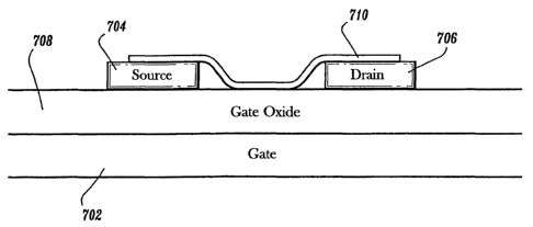
Referring to Fig. 7a, showing a small array of independently
addressable SWNT FETs fabricated using standard lithography. An array of
metallic pads (e. g., 701) is provided, each pad includes a source 704,
drain 706, or gate electrode 702. The substrate for these pads can be any
insulating material, preferably silica based. The combination of substrate
and metallic pads is referred to as the substrate for the nanotubes. Each
CA 02431064 2003-06-12
WO 02/054505 PCT/GBO1/05715
13
FET includes a source, a drain, a gate, and at least one nanotube
connecting the source and the drain. The nanotubes are provided to connect
each source to a corresponding drain. Referring now to Fig. 7b, a gate
oxide 708 separates the gate 702 from the electrodes (704, 706). The SWNT
density can be adjusted to ensure that at least one rope (e. g., 710)
shorts every set of electrodes while minimizing the unwanted connections
between devices. Preferably, the density of nanotubes has no thickness,
e.g., is less than a monolayer or 100% coverage. Some results have shown
that densities of less than one percent are sufficient to ensure that each
l0 source-drain pair is connected by at least one nanotube, though densities
as low as about 1/l0th of one percent of the substrate can also provide
connectivity for each source-drain pair in an array. Ropes between source
and drain electrodes (e. g., 710) are converted into FETs by selective
breakdown of metallic nanotubes, while stray nanotubes were removed
entirely by complete breakdown.
Although these ropes initially show little or no switching because
of their metallic constituents, final devices with good FET
characteristics can be reliably achieved as shown in Fig. 6d. Some results..
indicate that the generation of SWNT FETs can be achieved with greater
than 90o certainty from a disordered starting material. Fig. 6d summarizes.
results for thirty-two devices incorporating one or more SWNT ropes.
Before modification, e.g., 610, the conductance of individual ropes varies
widely due to the distribution of rope sizes as well as contact effects,
and very few devices can be substantially depleted by the gate.
Upon breaking the metallic SWNTs, the conductance of each rope is
decrease but the remaining channel is solely semiconducting and can be
fully depleted. The resulting devices have reasonable FET characteristics
limited primarily by contact resistance, a difficulty which is being
addressed separately. Multiple, small SWNT bundles can be produced by
chemical vapor growth and can alleviate the difficulties encountered with
large bundles and result in FETs having excellent conductivity and
switching ratios.
Although this application has focused on the particular system of
carbon nanotubes, the same principles may apply broadly to various
molecular electronics systems. In general, arrays of molecular devices can
be produced by design using external electrical means, without a need for
actual control at the nanometer scale. Discretionary modification allows
for the definition of useful electronic elements from a random mixture.
Although this solution has been applied to solve the problem of variation
inherent to carbon nanotubes, one skilled in the art would see in light of
CA 02431064 2003-06-12
WO 02/054505 PCT/GBO1/05715
14
the present disclosure that similar results can be achieved using miactures
of other molecules.
Having described embodiments of a system and method for engineering
carbon nanotubes and nanotube circuits using electrical breakdown, it is
noted that modifications and variations can be made by persons skilled in
the art in light of the above teachings. It is therefore to be understood
that changes may be made in the particular embodiments of the invention
disclosed which are within the scope and spirit of the invention as
defined by the appended claims. Having thus described the invention with
the details and particularity required by the patent laws, what is claimed
and desired protected by Letters Patent is set for in the appended claims.