Note: Descriptions are shown in the official language in which they were submitted.
CA 02431122 2003-06-05
ELECTRONIC BALLAST WITH ADAPTABLE
CHARGE PUMP POWER. FACTOR CORRECTION
Field of the Invention
The present invention relates to the general subject of circuits for
powering discharge lamps. More particularly, the present invention relates to
an
electronic ballast with adaptable charge pump power factor correction.
Background of the Invention
Fluorescent lighting systems are used extensively in industrial facilities
and office buildings. Usually, there is more than one lamp in each lighting
fixture, and one ballast powers each of those lamps. In a typical large
building,
the number of lighting fixtures can be in the hundreds or even thousands.
Although the amount of power drawn by each ballast is low (e.g., less than 150
watts), the total amount of power consumed by the fluorescent lighting in a
single building can reach in the tens of kilowatts. Such a large load can
create a
negative effect on the AC line, and potentially cause malfunction in sensitive
electrical devices such as computers, lab equipment, and medical devices. In
order to avoid such effects, there are rather high standards regarding the
"quality" of the power (and, thus, the current) drawn by ballasts from the AC
line. These standards are embodied in a number of front-end performance
requirements, including high power factor (PF), low harmonic distortion (HD),
and low line-conducted electromagnetic interference (EMI).
There are three main circuit approaches for providing the desired front-
end performance in an electronic ballast. Each has significant shortcomings.
First, there is the "passive" power factor correction (PFC) approach. The
circuitry in this approach consists essentially of an iron choke. The choke,
which has a high inductive impedance at the AC line frequency (e.g., 60
hertz),
typically provides a power factor of greater than 0.95 and a total harmonic
distortion of less than 20%. With the addition of "X" and "Y" capacitors, this
approach provides EMI suppression as well. The shortcomings of this approach
are high cost, large physical size, and high power dissipation.
CA 02431122 2003-06-05
2
A second approach is commonly referred to as "active" power factor
correction, which is usually realized by a high frequency boost type converter
comprising a MOSFET switch, a small ferrite inductor, and control circuitry
for
the MOSFET switch. Additionally, a small common-mode ferrite inductor with
X and Y capacitors is required for EMI suppression. This approach provides
close to unity power factor and a total harmonic distortion of less than 10%.
An
additional benefit of this approach is that the DC bus voltage (i.e., the
voltage
provided at the output of the boost converter) remains constant over
relatively
wide variations in input voltage or load. The shortcomings of this approach
include complex circuitry and high material cost.
A third approach is commonly referred to as "charge pump" power factor
correction (PFC), wherein high frequency current from the ballast inverter or
output is fed back to the front-end portion of the ballast. In its simplest
form, a
charge pump circuit consists of a single diode and capacitor; like the two
approaches previously described, this approach requires additional circuitry
for
EMI suppression. Properly designed and implemented, a charge pump circuit
can provide front-end performance comparable to that of a boost converter
(e.g.,
close to unity power factor and less than 10% total harmonic distortion), but
with considerably less cost, complexity, a nd physical size.
FIG. 1 schematically illustrates a prior art ballast with a charge pump
arrangement. The ballast 20 includes: an EMI filter 40; a full-wave diode
bridge
42,44,46,48; a charge pump circuit consisting of inductor 60, capacitor 62,
and
diode 52; an energy-storage capacitor 58; and a half-bridge inverter 70 that
includes two series-connected transistors 72,74 coupled at a junction 76. The
ballast is connected to the AC line source 10 via input connections 22,24, and
to
a fluorescent lamp 12 via output connections 26,32. During operation, the
charge-pump circuit works in conjunction with the inverter to increase the
power
factor of the current drawn from AC line source 10 by injecting an amount of
high frequency current from the inverter into the junction between diode
bridge
42,44,46,48 and diode 52. This injection of current also acts to boost the DC
bus voltage across capacitor 58; the DC bus voltage is dependent on the
inverter
operating frequency, the capacitance of capacitor 58, and the energy consumed
CA 02431122 2003-06-05
3
by lamp 12. During steady-state operation, there is a balance between the
energy
provided by the charge pump (to energy-storage capacitor 58) and the energy
consumed by the load (i.e., lamp 12).
A major shortcoming of charge pump circuits lies in the fact that the DC
bus voltage is strongly dependent on the load power. More specifically, the DC
bus voltage will tend to increase as the load decreases. For example, in the
case
of removal or failure of lamp 12 (or, in a ballast that power multiple lamps,
the
removal or failure of even one lamp), the DC bus voltage will jump to an
unacceptably high level, which can lead to inverter failure. Thus, ballasts
with
charge pump circuits necessarily include special protection circuitry for
dealing
with lamp removal/failure.
Known ballasts with charge pump PFC are intended to work with only
one or two lamps connected in series. In the case of lamp removal/failure, a
shutdown circuit stops ballast operation. This type of ballast is widely used
in
the European market, and ballast shutdown in the event of lamp removal/failure
is a required feature in Europe.
By contrast, in the North American market, the most widely used ballasts
operate anywhere from two to four lamps connected in parallel. Because it is
expected that the ballast will continue to operate even if some (but not all)
of the
lamps fail or are removed, a complete shutdown of the ballast in the event of
removal/failure of some of the lamps is not an acceptable option.
What is needed, therefore, is a ballast with charge pump power factor
correction that accommodates multiple parallel-connected lamps and that, in
the
event of removal/failure of some of the lamps, continues to provide power to
the
remaining lamps without harm to the ballast. A further need exists for a
ballast
that realizes the aforementioned functionality in an efficient and cost-
effective
manner. Such a ballast would represent a significant advance over the prior
art.
CA 02431122 2010-09-08
4
Accordingly, in one aspect of the present invention, there is provided a
ballast for
powering at least one gas discharge lamp, comprising: a pair of input
connections adapted
to receive a source of alternating current; a first output connection and a
return path
connection adapted for connection to a first gas discharge lamp; a full-wave
rectifier circuit
coupled to the input connections; an energy-storage capacitor operably coupled
to the full-
wave rectifier circuit; an inverter circuit operably coupled between the full-
wave rectifier
and the output connections; and a charge pump arrangement, comprising: a
charge pump
rectifier having an anode coupled to the full-wave rectifier circuit, and a
cathode coupled to
the energy-storage capacitor and the inverter; a first switching element
having a first
terminal coupled to the inverter, a second terminal coupled to the first
output connection, a
third terminal, and a fourth terminal, wherein the first switching element is
operable: (i) in
response to a nonzero current flowing through the first lamp, to couple the
third terminal to
the fourth terminal; (ii) in response to substantially no current flowing
through the first lamp,
to decouple the third terminal from the fourth terminal; a charge pump
inductor coupled
between the inverter node and the fourth terminal of the first switching
element; and a first
charge pump capacitor coupled between the anode of the charge pump rectifier
and the third
terminal of the first switching element.
In another aspect of the present invention, there is provided a ballast for
powering at
least one gas discharge lamp, comprising: a pair of input connections adapted
to receive a
source of alternating current; a first output connection and a return path
connection adapted
for connection to a first gas discharge lamp; a full-wave rectifier circuit
coupled to the input
connections; an energy-storage capacitor operably coupled to the full-wave
rectifier circuit;
an inverter circuit operably coupled between the full-wave rectifier and the
output
connections; and a charge pump arrangement, comprising: a charge pump
rectifier having
an anode coupled to the full-wave rectifier circuit, and a cathode coupled to
the energy-
storage capacitor and the inverter; a first switching element, comprising:
first, second, third,
and fourth terminals, wherein the first terminal is coupled to the inverter
and the second
terminal is coupled to the first output connection; a current transformer
having a primary
winding and secondary winding, wherein the primary winding is coupled between
the first
terminal and the second terminal, and the secondary winding is coupled between
a first node
and a common node, the common node being coupled to the fourth terminal; a
first resistor
coupled between the first node and the common node; a diode having an anode
coupled to
the first node and a cathode coupled to a second node; a capacitor coupled
between the
second node and the common node; a second resistor coupled between the second
node and
CA 02431122 2010-09-08
the common node; and a voltage-controlled switch having a gate coupled to the
second node,
a drain coupled to the third terminal, and a source coupled to the fourth
terminal; a charge
pump inductor coupled between the inverter node and the fourth terminal of the
first
switching element; and a first charge pump capacitor coupled between the anode
of the
5 charge pump rectifier and the third terminal of the first switching element.
In another aspect of the present invention, there is provided a ballast for
powering a
plurality of gas discharge lamps, comprising: a pair of input connections
adapted to receive
a source of alternating current; a plurality of output connections and a
return path
connection adapted for connection to the plurality of gas discharge lamps,
wherein each
lamp is connected between its corresponding output connection and the return
path
connection; a full-wave rectifier circuit coupled to the input connections; an
energy-storage
capacitor operably coupled to the full-wave rectifier circuit; an inverter
circuit operably
coupled between the full-wave rectifier and the output connections; a charge
pump rectifier
having an anode coupled to the full-wave rectifier circuit, and a cathode
coupled to the
energy-storage capacitor and the inverter; and a load-adaptable charge pump
arrangement
coupled between the inverter, the output connections, and the anode of the
charge pump
rectifier, the load-adaptable charge pump arrangement comprising: a charge
pump inductor;
a plurality of switching elements, wherein the plurality of switching elements
and the
plurality of gas discharge lamps are equal in number, such that each switching
element has a
corresponding gas discharge lamp, wherein each switching element has a first
terminal
coupled to the inverter, a second terminal coupled to the first output
connection, a third
terminal, and a fourth terminal, and wherein each switching element is
operable: (i) in
response to a nonzero current flowing through the corresponding gas discharge
lamp, to
couple the third terminal to the fourth terminal; (ii) in response to
substantially no current
flowing through the corresponding gas discharge lamp, to decouple the third
terminal from
the fourth terminal; and a plurality of charge pump capacitors, wherein the
plurality of
charge pump capacitors and the plurality of gas discharge lamps are equal in
number, such
that each charge pump capacitor has a corresponding gas discharge lamp and a
corresponding switching element, wherein each charge pump capacitor is coupled
between
the anode of the charge pump rectifier and the third terminal of the
corresponding switching
element, and wherein each charge pump capacitor in the plurality of charge
pump capacitors
is connected and operates only when its corresponding gas discharge lamp is
present in the
ballast and operating, creating a circuit path by which a charge pump
capacitor feeds high
CA 02431122 2010-09-08
5a
frequency current back into the anode of the charge pump rectifier when the
corresponding
discharge lamp is present and operating; the load-adaptable charge pump
arrangement thus
being operable to inject a high frequency current into the anode of the charge
pump rectifier,
wherein the high frequency current has a magnitude that is determined by the
number of
charge pump capacitors that are connected and operating and thus is dependent
on the
number of operating lamps present between the output connections and the
return path
connection.
Brief Description Of The Drawings
FIG. 1 describes a known ballast with charge pump power factor correction, in
accordance with the prior art.
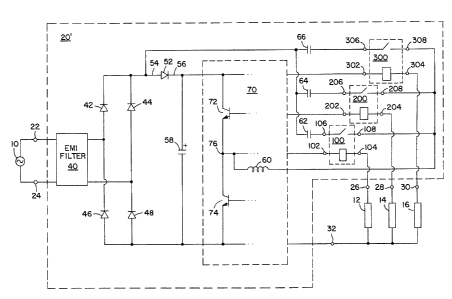
FIG. 2 describes a ballast with charge pump power factor correction, in
accordance
with a preferred embodiment of the present invention.
FIG. 3 describes a preferred circuit for implementing the switching elements
in the
ballast described in FIG. 2, in accordance with a preferred embodiment of the
present
invention.
Detailed Description of the Preferred Embodiments
FIG. 2 describes a ballast 20' for powering three gas discharge lamps
12,14,16.
Ballast 20' comprises a pair of input connections 22,24, a full-wave rectifier
circuit
42,44,46,48, an energy-storage capacitor 58, an inverter 70, first, second,
and third output
connections 26,28,30, and a return path connection 32. Ballast 20' further
comprises a
charge pump arrangement that includes a charge pump rectifier 52, a charge
pump inductor
60, first, second, and third charge pump capacitors 62,64,66, and first,
second, and third
switching elements 100,200,300.
Input connections 22,24 are adapted to receive a source of alternating
current, such
as 120 volts (rms) at 60 hertz. First, second, and third output connections
26,28,30 and
return path connection 32 are adapted for connection to first, second, and
third lamps
12,14,16; more specifically, first lamp 12 is connected between first output
connection 26
and return path connection 32, second lamp 14 is connected between second
output
connection 28 and return path connection 32, and third lamp 16 is connected
between third
output connection 30 and return path connection 32. Full-wave rectifier
circuit 42,44,46,48
CA 02431122 2010-09-08
5b
is coupled to input connections 22,24 via EMI filter 40. Energy-storage
capacitor 58 is
coupled to the full-wave rectifier circuit via charge pump rectifier 52.
Inverter 70 is coupled
to the full-wave rectifier (via charge pump rectifier 52) and output
connections 26,28,30,32.
Charge pump rectifier 52 has an anode 54 coupled to the full-wave rectifier,
and a
cathode 56 coupled to energy-storage capacitor 58 and inverter 70. Each
switching element
100,200,300 has four terminals. The first terminal 102,202,302 of each
switching element is
coupled to inverter 70, while the second terminal 104,204,304 of each
switching element is
coupled to a corresponding output connection 26,28,30; that is, second
terminal 104 (of
switching element 100) is coupled to first output connection 26, second
terminal 204 (of
to switching element 200) is coupled to second output connection 28, and
second terminal 304
(of switching element 300) is coupled to third output connection 30. Charge
pump inductor
is coupled between inverter 70 and the
CA 02431122 2003-06-05
6
fourth terminal 108,208,308 of each switching element 100,200,300. Finally,
each charge pump capacitor 62,64,66 is coupled between the anode 54 of charge
pump rectifier 52 and the third terminal 106,206,306 of its corresponding
switching element 100,200,300,
Each switching element 100,200,300 is operable: (i) in response to a
nonzero current flowing through its corresponding lamp, to couple the third
terminal to the fourth terminal; and (ii) in response to substantially no
current
flowing through its corresponding lamp, to decouple the third terminal from
the
fourth terminal. For example, if first lamp 12 is operating, first switching
element 100 will couple third terminal 106 to fourth terminal 108, thereby
creating a circuit path by which first charge pump capacitor 62 feeds high
frequency current back into the anode 54 of charge pump rectifier; on the
other
hand, if first lamp 12 is removed or failed, first switching element 100 will
not
coupled third terminal 106 to fourth terminal 108, thereby creating an open
circuit that prevents first charge pump capacitor 62 from feeding back any
high
frequency current. The same relationships apply to the switching elements
200,300 and the charge pump capacitors 64,66 that are associated with the
second and third lamps 14,16.
Switching elements 100,200,300 may be implemented via an
electromagnetic relay that is internally configured in a "normally open"
manner.
That is, with no current flowing into first terminal 102 and out of second
terminal 104, third and fourth terminals 106,108 are electrically decoupled
(i.e.,
the "switch" between third and fourth terminals 106,108 is open); conversely,
with current flowing into first terminal 102 and out of second terminal 104,
third
and fourth terminals 106,108 are electrically coupled (i.e., the "switch"
between
third and fourth terminals 106,108 is closed).
Ballast 20' provides a load-adaptable charge pump arrangement wherein
the magnitude of the high frequency current that is injected into the anode of
charge pump rectifier 52 is dependent on the number of operating lamps. As
long as all three lamps 12,14,16 are present and operating, all three charge
pump
capacitors 62,64,66 will be connected. Consequently, the high frequency
current that is fed back to the anode 54 of charge pump rectifier 52 will be
at its
CA 02431122 2003-06-05
7
maximum. If only two lamps are present and operating, only two of the three
charge pump capacitors will be connected, and the amount of high frequency
current that is fed back will be correspondingly less. As a consequence, the
DC
bus voltage will be prevented from significantly increasing following a
reduction in the load. Along similar lines, if only one lamp is present and
operating, the amount of current that is fed back will be even lower because
only
one charge pump capacitor remains connected. Finally, if no lamp remains
present and operating, there will be no current fed back because all of the
charge
pump capacitors are then disconnected. In this way, switching elements
100,200,300 ensure that the amount of high frequency current that is fed back
to
charge pump rectifier 52 is reduced as lamps fail or are removed.
As an alternative to implementation via an electromechanical relay, each
switching element 100,200,300 may be implemented via a suitable electronic
circuit arrangement, such as that which is illustrated in FIG. 3. As described
in
FIG. 3, the arrangement comprises a current transformer 110, a first resistor
120,
a diode 122, a capacitor 132, a second resistor 134, and a voltage-controlled
switch 140. Current transformer 110 has a primary winding 112 coupled
between first terminal 102 and second terminal 104, and a secondary winding
114 coupled between a first node 116 and a common node 118; common node
118 is itself coupled to fourth terminal 108. First resistor 120 is coupled
between first node 116 and common node 118. Diode 122 has an anode 124
coupled to first node 116, and a cathode 126 coupled to a second node 130.
Capacitor 132 and resistor 134 are each coupled between second node 130 and
common node 118. Voltage-controlled switch 140, which is preferably
implemented as a field-effect transistor, has a gate coupled to second node
142,
a drain 144 coupled to third terminal 106, and a source 146 coupled to fourth
terminal 108.
During operation, the current that flows through first lamp 12 (see FIG.
2) also flows through primary winding 112. Thus, when first lamp 12 is present
and conducting current, a nonzero current will flow through primary winding
112 and induce a voltage in secondary winding 114. The voltage across
secondary winding 114 is peak-detected by diode 122 and capacitor 132, and
CA 02431122 2003-06-05
8
then applied to the gate-source junction of transistor 140. This voltage
(e.g., 10
volts or so) causes transistor 140 to turn on and effectively connect third
terminal 106 to fourth terminal 108. If, on the other hand, first lamp 12 is
not
present or is not conducting current, zero current will flow through primary
winding 112. Correspondingly, no voltage will be induced in secondary
winding 114, so transistor 140 will be off and third terminal 106 will be
effectively disconnected from fourth terminal 108.
A prototype ballast configured substantially as shown in FIG. 2 was built
and tested. The AC line voltage was 277 volts at 60 hertz, the inverter
operating
frequency was set at 47 kilohertz, the capacitance of each charge pump
capacitor
was chosen to be 5.6 nanofarads, and the nominal load consisted of three 32
watt lamps. The DC bus voltage (Vbus), power factor (PF), total harmonic
distortion (THD), and lamp current crest factor (CF) were measured under
different load conditions. Those measurements are given below.
# of lamps Vbus (Vrms) PF THD (%) CF
3 415 0.986 2.89 1.65
2 412 0.974 8.96 1.60
1 380 0.924 23.0 1.52
0 379 -- -- --
It can thus be seen that ballast 20' accommodates parallel operation of
multiple lamps in a reliable manner while still providing a useful degree of
power factor correction in cases where one or more lamps is removed or failed.
Although the present invention has been described with reference to
certain preferred embodiments., numerous modifications and variations can be
made by those skilled in the art without departing from the novel spirit and
scope of this invention. For instance, it should be appreciated that the
principles
and advantages of the present invention are generally applicable to ballasts
with
two or more lamps. For example, the circuitry illustrated in FIG. 2 can be
modified to accommodate a fourth lamp simply by adding one additional output
connection, switching element, and charge pump capacitor. Similarly, the
CA 02431122 2003-06-05
9
circuitry in FIG. 2 can be modified to a two lamp ballast simply by omitting
output connection 30, switching element 300, and charge pump capacitor 66.
Moreover, although the principles of the present invention are most
advantageously applied to ballasts that power multiple lamps, it is believed
that
they are also applicable to ballasts that power a single lamp.
What is claimed is: