Note: Descriptions are shown in the official language in which they were submitted.
CA 02431185 2003-06-05
DIPOLE ARRANGEMENTS USING DIELECTRIC SUBSTRATES
OF META-MATERIAILS
BACKGROUND OF THE IN'~"ENTION
Statement of the Technical Fielel
The inventive arrangements relate generally to methods and
apparatus for providing increased design flexibility for RF circuits, and more
particularly for optimization of dielectric circuit board materials for
improved
performance.
Description of the Related Art
RF circuits, transmission lines and antenna elements are commonly
manufactured on specially designed substrate boards. For the purposes of these
types of circuits, it is important to maintain careful control over impedance
characteristics. If the impedance of different part: of the circuit do not
match,
this can result in inefficient power transfer, unnecessary heating of
components,
1 5 and ether problems. Electrical length at transmission lines and radiators
in these
circuits can also be a critical design factor.
Twa critical factors affecting the performance of a substrate
material are dielectric canstant (sometimes called 'the relative permittivity
or sr. )
and the loss tangent (sometimes referred to as the: dissipation factor). The
relative permittivity determines the speed of the signal in the substrate
material,
and therefore the electrical length of transmission lines and other components
implemented on the substrate. The loss tangent characterizes the amount of
loss that occurs for signals traversing the substrate material. Lasses tend to
increase with increases in frequency. Accordingly, law loss materials become
even more important with increasing frequency, particularly when designing
receiver front ends and low noise amplifier circuits.
Printed transmission lines, passive circuits and radiating elements
used in RF circuits are typically formed in one of three ways. One
configuration
known as rnicrostrip, places the signal line on a board surface and provides a
CA 02431185 2003-06-05
second conductive layer, commonly referred to as a ground plane. A second
type of configuration known as buried microstrip is similar except that the
signal
line is covered with a dielectric substrate material. In a third configuration
known as stripline, the signal line is sandwiched between two electrically
conductive (ground) planes. Ignoring losses, the characteristic impedance of a
transmission line, such as stripline or microstrip, i:~ equal to ~ LI~CI where
L, is
the inductance per unit length and Cl is the capacitance per unit length. The
values of LI and C~ are generally determined by the physical geometry and
spacing of the line structure as well as the permitltivity of the dielectric
materials) used to separate the transmission line structures. Conventional
substrate materials typically have a permeability of approximately 1 Ø
In convewtional RF design, a substrate material is selected that has
a relative permittivity value suitable for the design. Once the substrate
material
is selected, the line characteristic impedance value: is exclusively adjusted
by
1 5 controlling the line geometry and physical structure.
Radio frequency (RF) circuits are typically embodied in hybrid
circuits in which a plurality of active and passive circuit components are
mounted and connected together on a surface of an electrically insulating
board
substrate such as a ceramic substrate. The various components are generally
interconnected by printed metalBic conductors of copper, gold, or tantalum,
for
example that are transmission lines as stripline or microstrip or twin-line
structures.
The dielectric constant of the chosen substrate material for a
transmission line, passive RF device, or radiating element determines the
physical wavelength of RF energy at a given frequency for that line structure.
One problem encountered when designing microelectronic RF circuitry is the
selection of a dielectric board substrate material that is optimized for all
of the
various passive components, radiating elements and transmission line circuits
to
be formed on the board. In particular, the geometry of certain circuit
elements
may be physically large or miniaturized due to the unique electrical or
impedance
characteristics required for such elements. For example, many circuit elements
-2-
CA 02431185 2003-06-05
or tuned circuits may need to be an electrical 1 /4 wave. Similarly, the line
widths required for exceptionally high or low characteristic impedance values
can, in many instances, be too narrow or too wide for practical implementation
for a given substrate. Since the physical size of the microstrip or stripline
is
inversely related to the relative permittivity of the dielectric material, the
dimensions of a transmission line can be affected greatly by the choice of
substrate board material.
Still, an optimal board substrate material design choice for some
components may be inconsistent with the optimal board substrate material for
other components, such as antenna elements. Moreover, some design
objectives for a circuit component may be inconsistent with one another. For
example, it may be desirable to reduce the size of an antenna element. This
could be accomplished key selecting a board material with a relatively high
permittivity. However, the use of a dielectric witre a higher relative
permittivity
1 5 will generally have the undesired effect of reducing the radiation
efficiency of the
antenna.
An antenna design goal is frequently to effectively reduce the size
of the antenna without too great a reduction in radiation efficiency. One
method
of reducing antena size is through capacitive loading, such as through use of
a
high dielectric constant substrate for the dipole array elements.
For example, if dipole arms are capacitivel~% loaded by placing them
on °'high" dielectric constant board substrate portions, the dipole
arms can be
shortened relative to the arm lengths which would otherwise be needed using a
lower dielectric constant substrate. This effect results because the
electrical field
in high dielectric substrate portion between the arrn portion and the ground
plane
will be concentrated into a smaller dielectric substrate volume.
However, 'the radiation efficiency, being the frequency dependent
ratio of the power radiated by the antenna to the total power supplied to the
antenna will be reduced primarily due to the shorter dipole arm length. A
shorter
arm length reduces the radiation resistance, which is approximately equal to
the
-3-
CA 02431185 2003-06-05
square of the arm length for a °'short" (less the 1 /2 wavelength)
dipole antenna
as shown below:
R,. = 20 ~c 2 ( l/~, )2
where l is the electrical length of the antenna line; and ~, is the wavelength
of
interest.
A conductive trace comprising a single short dipole can be
modeled as an open transmission fine having series connected radiation
resistance, an inductor, a capacitor and a resistive: ground loss. The
radiation
efficiency of a dipole antenna system, assuming a single mode can be
approximated by the following equation:
Rr
E= -
~R,. + X~ + X~. + RI
Where
E is the efficiency
RY is the radiation resisi:ance
1 5 XL is the inductive reactance
X~ is the capacitive reactance
X~ is the ohmic feed point ground losses and skin effect
The radiation resistance is a fictitious resistance that accounts for
energy radiated by the antenna. The inductive reactance represents the
inductance of the conductive dipole lines, while the capacitor is the
capacitance
between the conductors, The other series connected components simply turn
RF energy into heat, which reduces the radiation efficiency of the dipole.
From the foregoing, it can be seen that the constraints of a circuit
board substrate having selected relative dielectric properties often results
in
-4-
CA 02431185 2003-06-05
design compromises that can negatively affect the electrical performance
and/or
physical characteristics of the overall circuit. An inherent problem with the
conventional approach is that, at least with respect to the substrate, the
only
control variable for line impedance is the relative permittivity. This
limitation
highlights an important problem with conventional substrate materials, i.e.
they
fail to take advantage of the other factor that detE:rmines characteristic
impedance, namely L~ , the inductance per unit length of the transmission
line.
Yet another problem that is encouni:ered in RF circuit design is the
optimization of circuit components for operation on different RF frequency
bands. Line impedances and lengths that are optimized for a first RF frequency
band may provide inferior performance when usedl for other bands, either due
to
impedance variations and/or variations in electrical length. Such limitations
can
limit the effective operational frequency range for a given RF system.
Conventional circuit board substrates are generally formed by
1 5 processes such as casting or spray coating which generally result in
uniform
substrate physical properties, including the dielectric constant. Accordingly,
conventional dielectric substrate arrangements for RF circuits have proven to
be
a limitation in designing circuits that are optimal ins regards to both
electrical and
physical size characteristics.
SUM(VI/~(~Y OF TFiE i111VEINTpON
The invention concerns a dipole antE;nna of reduced size and with
improved impedance bandwidth. The antenna is preferably formed on a
dielectric substrate having a plurality of regions, each having a
characteristic
relative permeability and permittivity. First and second dipole radiating
element
defining conductive paths can be selectively formed on first characteristic
regions of the substrate having a first characteristic permeability and first
permittivity. A reactive coupling element can be interposed between the dipole
radiating elements for reactively coupling the first dipole radiating element
to the
second dipole radiating element.
_5_
CA 02431185 2003-06-05
The reactive coupling element is coupled to a second characteristic
region of the substrate having a second permittivity and second permeability
for
providing a desired reactance value for the reactive coupling element. The
reactive element can be comprised of at feast one of a capacitor and an
inductor.
if the reactive element is comprised of a capacitor', the capacitive coupling
can
be provided as between adjacent ends of the dipole elements. The capacitive
coupling is at least partially determined by the second relative permittivity.
The first and second characteristic regions are different from a
third characteristic region of the substrate with regard to at least one of
permeability and permittivity. According to one a spect of the invention, at
least
one of a third permittivity and a third permeability of the third
characteristic
region are smaller in value, respectively, as compared to at least one of the
first
and second permittivity and permeability. Accordiing to c~ second as~aect of
the
invention, the third permittivity and third permeabillity are larger in value,
1 5 respectively, as compared to at least one of the first and second
permittivity and
permeability.
According to another aspect of the invention, a metal sleeve
element can be disposed on the second characteristic region of the substrate
for
inductively coupling adjacent ends of the dipole radiating elements. According
to
a preferred embodiment, the ends define an RF fe~:d point for the dipole
radiating
elements. The metal sleeve element can be comprised of an elongated metal
strip disposed adjacent to at least a portion of the dipole radiating
elements. In
any case, the inductive coupling is at least partially determined by the
second
relative permeability.
According to another aspect of the invention, the first permeability
and the second permeability can be controlled by the addition of mete-
materials
to the dielectric substrate. Alternatively, or in addition thereto, the first
permittivity and the second permittivity can be controlled by the addition of
mete-materials to the dielectric substrate.
The invention can also include other 'types of antennas formed on
dielectric substrates. According to an alternative embodiment, the antenna can
_g_
CA 02431185 2003-06-05
be comprised of at least one radiating element, such as a loop, defining a
conductive path and selectively formed on first characteristic regions of the
substrate having a first characteristic permeability and first permittivity.
One or
more reactive coupling elements can be interposed between portions of the
conductive path that are separated by a gap. The. reactive coupling element
can
be coupled to a second characteristic region of the substrate having a second
permittivity and second permeability for providing a desired reactance value
for
the reactive coupling element. Further, the first and second characteristic
regions can be different from a third characteristic: region of the substrate
with
regard to at least one of permeability and permittiwity.
BRIEF ~ESGi~IPTION ~F THE (DRAWINGS
Fig. 1 is a top view of are antenna ellement formed on a substrate
1 5 for reducing the size and improving the radiation efficiency of the
element.
Fig. 2 is a cross-sectional view of an antenna element of Fig. 1
taken along line 2-2.
Fig. 3 is a top view of an alternative: embodiment of the antenna
element in Fig. 1 and associated feed line circuitry.
Fig. 4 is a flow chart that is useful for illustrating a process for
manufacturing an antenna of reduced physical sizE: and high radiation
efficiency.
Fig. 5 is a top view of an alternative embodiment of the invention
in which a capacitor has been added between the antenna elements to improve
the impedance bandwidth.
Fig. 6 is a cross-sectional view of the alternative embodiment of
Fig. 5 taken along line 6-6.
Fig. 7 is a top view of a further alternative embodiment of the
invention in which a series of reactive elements have been interposed along
the
length of a loop radiating element.
Fig. 8 is a cross-sectional view of the alternative embodiment of
Fig. 7 taken along line 8-8.
_7_
CA 02431185 2003-06-05
Fig. 9 is a top view of another alternative embodiment of the
invention in which a sleeve element has been added.
Fig. 10 is a cross-section view of tine alternative embodiment of
Fig. 9 taken along lines 10-10.
DETAILED DESCRIPTION OF THE PREFERRED EMBODIMEfVTS
Low dielectric constant board materials are ordinarily selected for
RF designs. For example, polytetrafluoroethylene (PTFE; based composites such
as RT/duroid ~ 6002 (dielectric constant of 2.94; loss tangent of .009) and
RT/duroid ~ 5880 (dielectric constant of 2.2; loss tangent of .0007? are both
available from Rogers Microwave Products, Advanced Circuit Materials Division,
100 S. Roosevelt Ave, Chandler, AZ 85226. Both of these materials are
common board material choices. The above board materials provide dielectric
layers having relatively low dielectric constants wiith accompanying low loss
tangents.
However, use of conventional board materials can compromise the
miniaturization of circuit elements and may also comprornise some performance
aspects of circuits that can benefit from high dielectric constant layers. A
typical tradeoff in a communications circuit is between the physical size of
antenna elements versus efficiency. By comparison, the present invention
provides the circuit designer with an added level of flexibility by permitting
use
of a dielectric layer portion with selectively controlled permittivity and
permeability properties optimized for efficiency. This added flexibility
enables
improved performance and antenna element densii:y not otherwise possible.
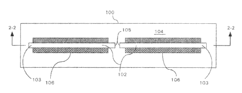
Referring to Fig. 1, antenna 102 cans be comprised of elements
103. The elements 103 can be mounted on dielectric layer 100 as shown or,
buried within the dielectric layer 100. fn Fig. 1, the antenna 102 is
configured
as a dipole, but it will be appreciated by those skillled in the art that the
invention
is not so limited. According to a preferred embodiment, dielectric layer 100
includes first region 104 having a first relative perrnittivity, and a second
region
106 having a second relative permittivity. The first relative permittivity can
be
_g_
CA 02431185 2003-06-05
different from the second relative permittivity, although the invention is not
so
limited. A ground plane 1 10 is preferably provided beneath the antenna 102
and
can include openings for the passage of antenna feeds 108. Alternatively, the
feed line for the antenna can be disposed directly on the surface of the
substrate
as shown in Fig. 3. Dielectric material 100 has a thickness that defines an
antenna height above ground. The thickness is approximately equal to the
physical distance from antenna 102 to the underlying ground plane 1 10.
Antenna elements 103 and the second region 106 of the dielectric
layer are configured so that at least a portion of tt~e antenna elements are
positioned on the second region 106 as shown. According to a preferred
embodiment, a substantial portion of each antenna element is positioned on the
second region 106 as shown.
In order to reduce the physical size of the elements 103, the
second relative permittivity of the substrate in the second region 106 can be
1 5 substantially larger than the first relative permittiv'ity of the
dielectric in the first
region 104. In general, resonant length is roughly proportional to 1 / ~Y
where
sF is the relative permittivity. Accordingly, selecting a higher value of
relative
permittivity can reduce the physical dimensions of the antenna.
One problem with increasing the relative permittivity in second
region 106 is that radiation efficiency of the antenna 102 can be reduced.
Microstrip antennas printed on high dielectric constant and relatively thick
substrates tend to exhibit poor radiation efficiency. With dielectric
substrate
having higher values of relative permittivity, a larger amount of the
electromagnetic field is concentrated in the dielectric between the conductive
antenna element and the ground plane. Poor radiation efficiency under such
circumstances is often attributed in part to surface: wave modes propagating
along the air/substrate interface.
As the size of the antenna is reduced through use of a high
dielectric substrate, the net antenna capacitance generally decreases because
the area reduction more than offsets the increase in effective permittivity
resulting from the use of a higher dielectric constaint substrate portion.
_g_
CA 02431185 2003-06-05
The present invention permits form<~tion of dielectric substrates
having one or more regions having significant magnetic permeability. Prior
substrates generally included materials having relative magnetic
permeabilities of
approximately 1. The ability to selectively add significant magnetic
permeability
to portions of the dielectric substrate can be used to increase the inductance
of
nearby conductive traces, such as transmission lines and antenna elements.
This flexibility can be used to improve RF system performance in a number of
ways.
For example, in the case of short dipole antennas, dielectric
substrate portions having significant relative magnetic permeability can be
used
to increase the inductance of the dipole elements to corr~pensate for losses
in
radiation efficiency from use of a high dielectric substrate and the generally
resulting higher capacitance. Accordingly, resonance can be obtained, or
approached, at a desired frequency by use of a diE;lectric having a relative
1 5 magnetic permeability larger than 1 . Thus, the invention can be used to
improve
performance or obviate 'the need to add a discrete inductor to the system in
an
attempt to accomplish the same function.
In generai it has been found that as substrate permittivity
increases from 1, it is desirable to also increase permeability in order for
the
antenna to more effectively transfer electromagnetic energy from the antenna
structure into free space. in this regard, it may beg noted that variation in
the
dielectric constant or permittivity mainly affects the electric field whereas
control
over the permeability improves the transfer of energy for the magnetic field.
For greater radiation efficiency, it has been found that the
permeability can be increased roughly in accordance with the square root of
the
permittivity. For example, if a substrate were selected with a permittivity of
9, a
good starting point for an optimal permeability would be 3. Of course, those
skilled in the art will recognize that the optimal values in any particular
case will
be dependent upon a variety of factors including the precise nature of the
dielectric structure above and below the antenna elements, the dielectric and
conductive structure surrounding the antenna elements, the height of the
-10-
CA 02431185 2003-06-05
antenna above the ground plane, width of the dipole arm, and so on.
Accordingly, a suitable combination of optimum values for permittivity and
permeability can be determined experimentally and/or with computer modeling.
Those skilled in the art will recognize that the foregoing technique
is not limited to use with dipole antennas such as those shown in Figs. 1 and
2.
Instead, the foregoing technique can be used to produce efficient antenna
elements of reduced size in other types of substrate structures. For example,
rather than residing exclusively on top of the substrate as shown in Fig. 1
and 2,
the antenna elements 103 can be partially or entirely embedded within the
second region 106 of the dielectric layer.
According to a preferred embodiment, the relative permittivity
and/or permeability of the dielectric in the second region 106 can be
different
from the relative permittivity and permeability of tike first region 104.
Further, at
least a portion of the dielectric substrate 100 can be comprised of one or
more
additional regions on which additional circuitry carp be provided. For
example, in
Fig. 3, region 1 12, 1 14, 1 16 can support antenna feed circuitry 1 15, which
can
include a balun, a feed line or an impedance transformer. Each region 1 12, 1
14,
1 16 can have a relative permittivity and permeability that is optimized for
the
physical and electrical characteristics required for each of the respective
components.
Likewise, these techniques can be used for any other type of
substrate antennas, the dipole of Fig. 1 being merely one example. Another
example is a loop antenna, as shown in Figs. 7 and 8, in which the
permittivity
and permeability of the substrate beneath the radiating elements and/or feed
circuitry is selectively controlled for reduced size ~nrith high radiation
efficiency.
In Fig. 7 a loop antenna element 700 having a feed point 506 and a matching
balun 705 is shown mounted on a dielectric substrate 701. A ground plane 703
can be provided beneath the substrate as illustrated. According to a preferred
embodiment, the dielectric substrate region 704 bE:neath the loop antenna
element 700 can have a permittivity and permeability that is different from
the
surrounding substrate 701 . The increased permittivity in region 704 can
reduce
-11-
CA 02431185 2003-06-05
the size of the antenna element 700 for a given operating frequency. In order
to
maintain satisfactory radiation efficiency however, the permeability in region
704
can be increased in a manner similar to that described above with respect to
the
dipole antenna.
Alternatively, or in addition to, the modifications to the dielectric
substrate beneath the antenna elements, other features of antenna performance
can be improved by advantageously controlling the characteristics of selected
portions of the substrate. For example, in conventional dipole antenna
systems,
it is known that a chip capacitor can be connected between the adjacent ends
of
the two antenna elements. The addition of a capacitor bridging the antenna
elements in this location is advantageous as it cans improve the impedance
bandwidth of the antenna. Those skilled in the arit are generally familiar
with the
techniques for selection of a suitable value of capacitance for achieving
performance improvements. However, as operating frequencies increase, the
1 5 necessary value of the coupling capacitor that would need to be provided
between the adjacent ends can become extremely small. The result is that the
proper capacitance value cannot be achieved using conventional lumped circuit
components, such as chip capacitors.
Referring to Fig. 1, a certain amount of capacitance will inherently
exist between the adjacent ends 105. However, the spacing of the ends 105
and the relatively low permittivity of the substrate 100 will generally be
such
that this inherent capacitance will not be the value necessary for optimizing
the
impedance bandwidth necessary for a particular application. Accordingly, Fig.
5
is a top view of an alternative embodiment of the invention in which the
permittivity in region 500 can be selectively contrc~lied. F=ig. 6 is a cross-
sectional view of the alternative embodiment of Fi<~. 5 taken along line 6-6.
Common reference numbers in Figs. 1-2 and 5-6 are used to identify common
elements in Figs. 5 and 6.
By selectively controlling the permittivity of the substrate in the
region 500 as shown, it is possible to increase or clecrease the inherent
capacitance that exists between the ends 105 of dipole elements 103. The
-12-
CA 02431185 2003-06-05
result is an improved impedance bandwidth that cannot otherwise be achieved
using conventional lumped element means. The limits of region 500 are shown
in Figs. 5 and 6 as extending only between the adjacent ends 105 of the
antenna elements 103. It will be appreciated by those skilled in the art that
the
invention is not so limited. Rather, the limits of region 500 can extend
somewhat more or less relative to the ends of the dipole elements 105 without
departing from the intended scope of the invention. For example, the region
500
can include a portion of the region below the ends of antenna elements 105.
Alternatively, only a portion of the region between the ends 105 can be
modified
so as to have different permittivifiy characteristics.
A similar technique for improving the impedance bandwidth can
also be applied to loop antennas. In the case of loop antennas, it is
conventional
to interpose capacitors along the conductive path defining the radiating
element
for the loop. In a conventional loop antenna, the referenced capacitors would
1 5 typically be connected between adjacent end portions 702 of antenna
element
700 as shown in Figs. 7 and 8. (However, as the design frequency of the
antenna increases, the capacitor values necessary to implement these
techniques can become too small to permit use of lumped element components
such as chip capacitors.
According to a preferred embodiment shown in Fig. 7 and 8, the
permittivity in regions 708 can be selectively controlled to adjust the
inherent
capacitive coupling that exists between end portions 702. For example, if the
permittivity of the substrate in regions 708 is increased, the inherent
capacitance between ends 702 can be increased. In this way, the necessary
capacitance can be provided to improve the impedance bandwidth by making
use of, and selectively controlling, the inherent capacitance between end
portions 702. Those skilled in the art will appreciate that the region 708 can
be
somewhat smaller than, or can extend somewhat past, the limits defined by end
portions 702.
Another alternative embodiment of the invention is illustrated in
Figs. 9 and 10 where dipole elements 902 are mounted on a substrate 900.
-13-
CA 02431185 2003-06-05
Dipole elements 902 can have a feed point 901 as is well known in the art. A
ground plane 904 can be provided beneath the substrate as shown, It is known
in the art that improvements to the input impedance bandwidth of an antenna
can be achieved by the use of capacitive and inductive coupling at the
adjacent
ends of dipole elements. In Figs. 9 and 10, this capacitive coupling is
achieved
using a modified dielectric region 906 with a higher permittivity as compared
to
surrounding substrate 900. This higher permittivity can improve capacitive
coupling between dipole elements 902 in much the same way as previously
described relative to Figs. 5 and G.
Further, the invention can make use of a conventional sleeve
element 908 to provide inductive coupling. According to a preferred
embodiment, however, the permeability of the modified dielectric region 906
can
be selectively controlled. For example, the permeability can be increased to
have a value larger than 1 . Alternatively, the permeability in region 906 can
be
1 5 controlled so as to vary along the length of the inductive element 908. In
any
case, the coupling between the "sleeve" and the dipole arm can be improved
and controlled by selectively adjusting the dielectric of the substrate
between
the sleeve and the dipole arm to improve the impedance bandwidth. The
incorporation of permeable materials beneath the sleeve would allow for the
control of line widths that might not otherwise be achievable without the use
of
magnetic materials. This control over the permittivity and permeability can
provide the designer with greater flexibility to provide improved broadband
impedance matching.
The inventive arrangements for integrating reactive capacitive and
inductive components into a dielectric circuit board substrate are not limited
for
use with the antennas as shown. Rather, the invention can be used with a wide
variety of other circuit board components requiring small amounts of carefully
controlled inductance and capacitance.
Dielectric substrate boards having metamaterial portions providing
localized and selectable magnetic and dielectric properties can be prepared as
shown in Fig. 4. In step 410, the dielectric board material can be prepared.
In
-14-
CA 02431185 2003-06-05
step 420, at least a portion of the dielectric board material can be
differentially
modified using meta-materials, as described below, to reduce the physical size
and achieve the best possible efficiency for the antenna elements and
associated
feed circuitry. Finally, a metal layer can be applied to define the conductive
traces associated with the antenna elements and associated feed circuitry.
As defined herein, the term "metamaterials" refers to composite
materials formed from the mixing or arrangement of two or more different
materials at a very fine level, such as the Angstrom or nanometer level.
Metamaterials allow tailoring of electromagnetic properties of the composite,
which can be defined by effective electromagnetic parameters comprising
effective electrical permittivity (or dielectric constantl and the effective
magnetic
permeability.
The process for preparing and differentially modifying the dielectric
board material as described in steps 410 and 420 shall now be described in
some
-15-
CA 02431185 2003-06-05
detail. It should be understood, however, that the methods described herein
are
merely examples and the invention is not intended to be so limited.
Appropriate bulk dielectric substrate materials can be obtained
from commercial materials manufacturers, such as DuPont and Ferro. The
unprocessed material, commonly called Green Tape", can be cut into sized
portions from a bulk dielectric tape, such as into 6 inch by 6 inch portions.
For
example, DuPont Microcircuit Materials provides Green Tape material systems,
such as Low-Temperature Cofire Dielectric Tape. These substrate materials can
be used to provide dielectric layers having relatively moderate dielectric
constants with accompanying relatively low loss tangents for circuit operation
at
microwave frequencies once fired.
In the process of creating a microwave circuit using multiple
sheets of dielectric substrate material, features such as vias, voids, holes,
or
cavities can be punched through one or more layers of tape. Voids can be
defined using mechanical means (e.g. punch) or directed energy means (e.g.,
laser drilling, photolithography), but voids can also be defined using any
other
suitable method. Some vias can reach through the entire thickness of the sized
substrate, while some voids can reach only through varying portions of the
substrate thickness.
The vias can then be filled with metal or other dielectric or
magnetic materials, or mixtures thereof, usually using stencils for precise
placement. The individual layers of tape can be stacked together in a
conventional process to produce a complete, multi-layer substrate.
The choice of a me~tamaterial composition can provide effective
dielectric constants over a relatively continuous range from less than 2 to
about
2650. Materials with magnetic properties are also available. For example,
through choice of suitable materials the relative effective magnetic
permeability
generally can range from about ~ to 1 16 for most practical RF applications.
However, the relative effective magnetic permeability can be as low as about 2
or reach into the thousands.
The term "differentially modified" as used herein refers to
-16-
CA 02431185 2003-06-05
modifications, including dopants, to a dielectric substrate layer that result
in at
least one of the dielectric and magnetic properties being different at one
portion
of the substrate as compared to another portion. A differentially modified
board
substrate preferably includes onE: or more metamaterial containing regions.
For example, the modification can be selective modification where
certain dielectric layer portions are modified to produce a first set of
dielectric or
magnetic properties, while other dielectric layer portions are modified
differentially or left unmodified to provide dielectric andlor magnetic
properties
different from the first set of properties. Differential modification can be
accomplished in a variety of different ways.
According to one embodiment, a supplemental dielectric layer can
be added to the dielectric layer. Techniques known in the art such as various
spray technologies, spin-on technologies, various deposition technologies or
sputtering can be used to apply the supplemental dielectric layer. The
1 5 supplemental dielectric layer can be selectively added in localized
regions,
including inside voids or holes, or over the entire existing dielectric layer.
For
example, a supplemental dielectric layer can be used for providing a substrate
portion having an increased effective dielectric constant.
The differential modifying step can further include locally adding
additional material to the dielectric layer or supplemental dielectric layer.
The
addition of material can be used to further control the effective dielectric
constant or magnetic properties of the dielectric layer to achieve a given
design
objective.
The additional material can include a plurality of metallic and/or
ceramic particles. Metal particles preferably include iron, tungsten, cobalt,
vanadium, manganese, certain rare-earth metals, nickel or niobium particles.
The particles are preferably nanorneter size particles, generally having sub-
micron physical dimensions, hereafter referred to as nanoparticles.
The particles, such as nanoparticles, can preferably be
organofunctionalized composite particles. For example, organofunctionalized
composite particles can include particles having metallic cores with
electrically
CA 02431185 2003-06-05
insulating coatings or electrically insulating cores with a metallic coating.
Magnetic metamateriai particles that are generally suitable for controlling
magnetic properties of dielectric layer for a variety of applications
described
herein include ferrite organoceramics (FexCyHz)-(Ca/Sr/Ba-Ceramic). These
particles work well for applications in the frequency range of 8-40 GHz.
Alternatively, or in addition thereto, niobium organoceramics (NbCyHz)-
(Ca/Sr/Ba-Ceramic) are useful for the frequency range of 12-40 GHz. The
materials designated for high frequency are also applicable to low frequency
applications. These and other types of composite particles can be obtained
commercially.
In general, coated particles are preferable for use with the present
invention as they can aid in binding with a polymer (e.g. LCP) matrix or side
chain moiety. In addition to controlling the magnetic properties of the
dielectric,
the added particles can also be used to control the effective dielectric
constant
of the material. Using a fill ratio of composite particles from approximately
1 to
70%, it is possible to raise and possibly lower the dielectric constant of
substrate dielectric layer and/or supplemental dielectric layer portions
significantly. For example, adding organofunctionalized nanoparticles to a
dielectric layer can be used to raise the dielectric constant of the modified
dielectric layer portions.
Particles can be applied by a variety of techniques including
polyblending, mixing and filling with agitation. For example, if the
dielectric
layer includes a LCP, the dielectric constant may be raised from a nominal LCP
value of 2 to as high as 10 by using a variety of particles with a fill ratio
of up to
about 70%.
Metal oxides useful for this purpose can include aluminum oxide,
calcium oxide, magnesium oxide, nickel oxide, zirconium oxide and niobium (Ii,
IV and V) oxide. Lithium niobate (LiNbOa), and zirconates, such as calcium
zirconate and magnesium zirconate, also may be used.
The selectable dielectric properties can be localized to areas as
small as about 10 nanometers, or cover large area regions, including the
entire
-18-
CA 02431185 2003-06-05
board substrate surface. Conventional techniques such as lithography and
etching along with deposition processing can be used for localized dielectric
and
magnetic property manipulation.
Materials can be prepared mixed with other materials or including
varying densities of voided regions (which generally introduce air) to produce
effective dielectric constants in a substantially continuous range from 2 to
about
2650, as well as other potentially desired substrate properties. For example,
materials exhibiting a low dielectric constant ( < 2 to about 4) include
silica with
varying densities of voided regions. Alumina with varying densities of voided
regions can provide a dielectric constant of about 4 to 9. Neither silica nor
alumina have any significant magnetic permeability. However, magnetic
particles can be added, such as up to 20 wt. %, to render these or any other
material significantly magnetic. f=or example, magnetic properties may be
tailored with organofunctionaiity. The impact on dielectric constant from
adding
magnetic materials generally results in an increase in the dielectric
constant.
Medium dielectric constant materials have a dielectric constant
generally in the range of 70 to 500 +l- 10%. As noted above these materials
may be mixed with other materials or voids to provide desired effective
dielectric
constant values. These materials can include ferrite doped calcium titanate.
Doping metals can include magnesium, strontium and niobium. These materials
have a range of 45 to 600 in relative magnetic permeability.
For high dielectric constant applications, ferrite or niobium doped
calcium or barium titanate zirconates can be used. These materials have a
dielectric constant of about 2200 to 2650. Doping percentages for these
materials are generally from about 1 to 10 %. As noted with respect to other
materials, these materials may be mixed with other materials or voids to
provide
desired effective dielectric constant values.
These materials care generally be modified through various
molecular modification processing. Modification processing can include void
creation followed by filling with materials such as carbon and fluorine based
organo functional materials, such as polytetrafluoroethylene PTFE.
-19-
CA 02431185 2003-06-05
Alternatively or in addition to organofunctionaf integration,
processing can include solid freeform fabrication (SFF), photo, uv, x-ray, e-
beam
or ion-beam irradiation. Lithography can also be performed using photo, uv, x-
ray, e-beam or ion-beam radiation.
Different materials, including metamaterials, can be applied to
different areas, so that a plurality of areas of the substrate layers have
different
dielectric andlor magnetic properties. The backfill materials, such as noted
above, may be used in conjunction with one or more additional processing steps
to attain desired, dielectric and/or magnetic properties, either locally or
over a
bulk substrate portion.
A top layer conductor print is then generally applied to tlhe
modified substrate layer. Conductor traces can be provided using thin film
techniques, thick film techniques, electroplating or any other suitable
technique.
The processes used
-20-
CA 02431185 2003-06-05
to define the conductor pattern include, but are not limited to standard
lithography and stencil.
A base plate is then generally obtained for collating and aligning a
plurality of modified board substrates.
The plurality of layers of substrate can then be laminated (e.g.
mechanically pressed) together using either isostatic pressure, which puts
pressure on the material from all directions, or uniaxial pressure, which puts
pressure on the material from only one direction. The laminate substrate is
then
is further processed as described above or placed into an oven to be fired to
a
temperature suitable for the processed substrate (approximately 850 C to 900 C
for the materials cited above).
The plurality of ceramic tape layers can be controlled to rise in
temperature at a rate suitable for the substrate materials used. The process
conditions used, such as the rate of increase in temperature, final
temperature,
1 5 cool down profile, and any necessary holds, are selected mindful of the
substrate material and any material deposited thereon. Following firing,
stacked
substrate boards, typically, are inspected for flaws using an optical
microscope.
The stacked ceramic substrates can then be optionally diced into
cingulated pieces as small as required to meet circuit functional
requirements.
Following final inspection, the cinguiated substrate pieces can then be
mounted
to a test fixture for evaluation of their various characteristics, such as to
assure
that the dielectric, magnetic and/or electrical characteristics are within
specified
limits.
Thus, dielectric substrate materials can be provided with localized
tunable dielectric and/or magnetic characteristics for improving the density
and
performance of circuits. The dielectric flexibility allows independent
optimization
of the feed line impedance and dipole antenna elements.
-21-