Note: Descriptions are shown in the official language in which they were submitted.
CA 02431463 2007-01-08
-1-
Monitoring And Correcting Bragg Gratings During Their Fabrication
Back rg ound
This invention relates to the process of correcting for phase errors during
the
fabrication of Bragg gratings.
Bragg gratings in optical waveguides (fiber and planar) are used for a variety
of
optical processing functions. The most common application is simple wavelength
filtering
in dense wavelength-division multiplexing (DWDM) systems.
In such applications, the ideal Bragg grating filter has a spectral response
that is
rectangular in shape, with sharp edges and a flat top. In general, any phase
or amplitude
errors in the fabrication process lead to a non-ideal spectral response.
Moreover, as the DWDM channel spacing becomes smaller, the filter bandwidth
must also be reduced by the same amount. The reduced bandwidth requires the
Bragg
grating lengths to increase. These requirements lead to a significantly
increased sensitivity
in the spectral quality of the filter to any errors in the fabrication
process. One common
source of such errors is the imperfection of the phase masks used in the
fabrication process.
More generally, any filter response will be negatively affected by the
presence of
errors in the fabrication process. In general, the longer the grating, the
more sensitive it will
be to errors.
A process that can eliminate or reduce the effect of these errors is desirable
and will
become more valuable as more complex optical processing functionality is
required.
Summary of the Invention
Accordingly, it is an object of this invention to at least partially overcome
some of
the disadvantages of the prior art.
Accordingly, in one of its aspects, this invention resides in a method of
writing a
Bragg grating in a waveguide comprising: exposing the waveguide to a Bragg
grating
writing beam; and correcting a phase error in the Bragg grating being written
by providing
relative movement between a phase mask used to write the Bragg grating and the
waveguide, the relative movement generating a phase correction of the same
magnitude but
opposite direction as the detected phase error.
CA 02431463 2007-01-08
- la-
Further aspects of the invention will become apparent upon reading the
following
detailed description and drawings, which illustrate the invention and
preferred embodiments
of the invention.
Brief Description of the Drawings
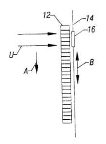
Figure 1 is a schematic depiction of one embodiment of the present invention;
Figure 2 is a graph showing the results with one embodiment of the present
invention
indicated at C and the results with a typical prior art embodiment indicated
at D;
Figure 3 is a schematic depiction of another embodiment of the present
invention;
Figure 4 is a schematic block diagram of an apparatus configured for measuring
amplitude and phase contributions to an output field; and
Figure 5 is a flow chart for one embodiment of the present invention.
CA 02431463 2003-06-09
-2-
Detailed Description
In accordance with one embodiment shown in Figure 1, a phase correction
process
involves shifting the interference pattern that illuminates a waveguide 14 as
the ultraviolet
writing beam U is scanned along the waveguide 14. The ultraviolet writing beam
U exposes
a phase mask 12. In one embodiment, the ultraviolet writing beam U may be
scanned along
the length of the mask 12 as indicated by the arrow A. At the position of the
writing beam U
shown in Figure 1, a grating 16 is formed in a waveguide 14. The waveguide 14
may be fiber
or may be a planar waveguide, as two examples.
The phase correction process may achieve the proper shift of the interference
pattern
by making small adjustments, indicated by the arrows B, to the relative
position, with respect
to the waveguide 14, of one or more of the phase gratings (e.g., masks) 12
used to generate
the interference pattern as the writing beam U is scanned along the waveguide
14. The
magnitude and direction of the shift is directly related to the error function
that is to be
corrected.
Typical phase errors in the phase masks 12 used in waveguide Bragg grating
production are on the order of several radians across the length of the
grating 16. This
translates into shifting the interference pattern by a few microns over the
length of the grating
16 in order to compensate for these errors.
The resolution with which the phase errors can be reduced is limited by both
the
position resolution of the stage used for shifting the interference pattern
and the size of the
beam U used for writing the Bragg grating 16. The better the stage resolution
and the smaller
the writing beam U, the more precisely one can control the phase of the
correction process.
Typically, nanometer resolution and control are used for the positioning of
the waveguide 14
with respect to the phase mask 12.
Referring to Figure 2, a graph of reflectivity versus wavelength for a
grating, in
accordance with the prior art, is indicated at D and for grating 116, in
accordance with one
embodiment of the present invention, is indicated at C. By correcting phase
mask error, a
higher quality grating can be produced with a narrower spectrum, as indicated
C in Figure 2,
in accordance with some embodiments of the present invention. In addition to
the correction
of errors associated with phase masks and translation stages used in the
fabrication of Bragg
gratings using standard phase mask methods, phase correction according to
embodiments of
the present invention may also be utilized in more advanced methods. For
example, in a
CA 02431463 2007-01-08
-3-
three-grating interferometric technique for Bragg grating fabrication, the
Bragg grating
wavelength may be tuned without changing any of the phase masks by any one of
several
means. One such method involves placing prisms or wedges 118, 119 in each arm
of the
interferometer 100 as shown in Figure 3. Rotation of the prisms or wedges 118,
1191eads to
a change in the period of the interference pattern and thus a corresponding
change in the
Bragg grating 116 wavelength.
The apparatus 100 includes a laser 101 (or other light source) that produces a
laser
beam 102 that is incident to a first diffraction grating 104 having a period
Apm. Diffraction
orders 106, 107 (the +1 and -1 diffraction orders, respectively) are produced
and directed to
respective gratings 108, 109 that have grating periods of about Apm/2. The
gratings 108, 109
may have grating periods ranging from about 80%-120% of Apm/2 in some
embodiments.
An undiffracted component I 11 of the beam 102 is blocked by a baffle 110.
A diffraction order 114 (a-1 order) produced by the grating 108 and a
diffraction order
115 (a+l order) produced by the grating 109 are directed to circular,
rotatable wedges or
prisms 118 and 119. In one embodiment, the wedges 118 and 119 are arranged so
that their
bisector is normal to the direction of propagation of light from a grating
108, 109 to a
waveguide 112. The intersecting angle of the two orders 114, 115 (at the
interference pattern
116) and, thus, the spatial frequency, of a Bragg grating being written in a
waveguide 112 is
modified by rotating the wedges or prisms 118 and 119 in opposite directions
indicated by
the arrows 121, 122 along an axis that is parallel to the propagation
direction of the light.
This process introduces a small amount of translation in the position of the
beam
intersection which may be compensated by translation of the waveguide 112 as
indicated by
the arrows E. For this purpose, the optical system 10 or the waveguide 112 may
be mounted
on a translation stage 117. In some implementations of this technique, a phase
shift
accumulates as the grating 116 is written which can distort the grating
spectrum. Generally,
the phase shift is linear with position along the grating 116 and the slope of
phase shift versus
position increases as the interferometer 100 is tuned away from its natural
wavelength
(determined by the phase masks). This type of phase error may be compensated
using the
process described above for phase mask error correction. Because of the
flexibility of the
three-grating interferometer, it is possible to employ other methods to
achieve phase
correction in addition to, or instead of, the process described above. For
example, because
the wedges modify the phase of the light that passes through them, it is
possible to shift the
CA 02431463 2003-06-09
-4-
phase of the exposure fringe pattern, and thus the phase of the Bragg grating,
by
appropriately rotating the two wedges. In this case, the wedges should be
rotated in the same
direction as opposed to the opposite direction as required for tuning the
frequency of the
Bragg grating, as described above. The degree and direction of the rotation
depends on the
specific phase error profile that is being corrected. Another method for
implementing phase
correction in the three-grating interferometer involves placing optical phase
modulators in
one or both arms of the interferometer. These devices serve to modify, in a
prescribed
manner, the optical phase of the light passing through them. Therefore, by
applying the
appropriate control signals to the phase modulators, one may shift the Bragg
grating phase in
such a way to correct for a known phase error profile. Other sources of phase
errors
associated with optical and/or mechanical components or procedures used in the
fabrication
of Bragg gratings, once quantified, may be eliminated or reduced using
embodiments of the
present invention.
Even if the source of a phase error is not known a priori, it is still
possible to use the
methods of the type described herein to correct or compensate for these
errors. In such cases
when the specific phase error function is not known prior to the fabrication
of the grating, one
may use other means to determine or estimate this quantity. One such method
involves
performing various measurements on the Bragg grating, either during
fabrication or after the
grating has been written. Determination of the appropriate optical properties
of the Bragg
grating can yield information about the phase profile of the grating and thus
may permit
reconstruction of the phase error function present during exposure of the
grating.
There are a variety of methods that can be used to determine the phase
function, and
thus the phase error, of a Bragg grating. Generally, optical phase is not a
directly detectable
quantity. Therefore, the methods for the determination of optical phase rely
on indirect
means that can be generally labeled coherent (or phase-sensitive) and
incoherent. Coherent
methods are typically more accurate and more direct since they are sensitive
to the phase of
the signal being measured (although they do not directly measure the phase).
However, they
are generally difficult to implement mainly because they involve
interferometric
measurements, which can be extremely sensitive to environmental effects. Two
such
examples of coherent phase measurements that may be used to determine the
phase function
of a Bragg grating are spectral interferometry and Fourier Transform
spectrometry. Both
CA 02431463 2003-06-09
-5-
methods have been applied to a wide variety of optical measurements and are
known in the
art.
Incoherent methods are generally less accurate and less direct, but they are
much
easier to implement since they involve easily measurable quantities, such as
spectral intensity
and temporal response of the device. However, since neither of these
quantities uniquely
depends on the optical phase, it is more difficult to determine the phase from
them. Thus, in
order to obtain the phase from incoherent methods, a phase extraction process
may be used.
The details of the phase extraction process depend on the types of data about
the device that
are available. In general, the more data that is available, the simpler the
phase extraction
process and the more accurate the result. Ideally, both the spectral and
temporal response of
the device is available. In this case, it is possible to use phase retrieval
algorithms in order to
extract the phase of the device. The specific algorithm for phase retrieval
for Bragg gratings
is a modified version of similar algorithms that are known in the art. In
cases where only
spectral or temporal responses are known, one may use other information about
the grating in
order to obtain the phase. A method that is well suited for Bragg gratings is
one where only
the spectral response is measured, using for example a tunable laser source
and a
photodetector to measure the reflected power from the grating versus
wavelength. The
spectral response by itself may not be sufficient to determine the phase
function of the
grating; however, because the fabrication of the grating involves scanning the
exposure beam
along the length of the phase mask or masks, one may measure the spectral
response for
different length gratings. One may use the set of spectral responses for
different lengths in
conjunction with a phase extraction process to obtain an estimate of the phase
function of the
grating. This method is not exact, however it is easy to implement and
requires a minimum
of additional measurements to be made in ordei to obtain an approximate phase
function for
the grating.
Depending on the method used to determine the phase function, it may be
defined in
any one of several ways, e.g., phase versus wavelength, phase versus time, or
phase versus
position along the grating. Since the phase correction process inherently
works in the space
domain, one may use the phase versus position in order to determine the phase
error function.
If, however, the phase extraction process yields a different phase function,
it is still possible
to convert it to the desired phase versus position function using techniques
known in the art.
CA 02431463 2007-01-08
-6-
Once the phase versus position of the grating is determined, by any of the
methods
described herein or any other method, then the phase error function is
obtained by simply
comparing the measured phase function with the specific spatial phase function
that was
designed for the grating. In many cases, the desired phase function is a
linear function across
the grating (a so-called "transform-limited" grating), in which case, the
phase variation
determined from the phase extraction process is equal to the phase error
function. Note that
the linear component of the phase function is generally not relevant for phase
correction and
thus may be removed. In general, however, the designed phase function may be
arbitrary.
For example, for dispersion compensating gratings, the designed phase function
may be
quadratic versus position. Whatever the form of the designed phase function,
the phase error
function is obtained by subtracting the extracted phase function from the
designed phase
function. The result is the phase error function that is used in the
correction process.
The correction process proceeds as described earlier using the phase error
function,
either directly measured (or known a priori using other means), or extracted
from
measurements on the grating itself as described above. Specifically, a phase
correction is
applied to the grating, as it is written, that is equal and opposite to the
phase error. The effect
of the phase correction is to remove or compensate the phase errors present in
the fabrication
process. Therefore, for a transform-limited grating, only the phase correction
function is
applied. For gratings with more complex designed phase profiles, the designed
phase
function must be added to the phase correction function before being applied
to the grating.
With reference to Figure 4, an apparatus 200 configured for characterizing or
measuring spatially dependent amplitude and phase contributions to an optical
field incident
to an optical element 202, such as a diffraction grating or phase mask. The
apparatus 200
may be used to quantify the phase error so that the error may then be
corrected as already
described. The apparatus 200 may include an aperture plate 203 that defines
slits 204, 205.
In one embodiment, a well collimated optical source 206, such as a laser beam
from a 1mW
frequency stabilized He-Ne laser (not shown) at a wavelength k=633 nm, is
expanded,
collimated, and directed incident at an angle 0 to normal to the element 202.
A lens 208 is
situated to receive optical radiation from slits 204, 205 and direct the
radiation to a detector
array 210 placed at a focal plane 211 of the lens 208. In an example, the
slits 204, 205 are
situated approximately 5 mm behind the element 202 and the lens 208 is a plano-
convex lens
having a Im focal length. The lens 208 is situated to direct a first order
diffracted beam to
the detector
CA 02431463 2003-06-09
-7-
array 210. In a particular embodiment, the detector array 210 is a HAMAMATSU
S3903-
256Q diode array that includes 256 detector elements having a pixel size of 25
m by 500
m. The diode array is controlled using a HAMAMATSU 4070 driver amplifier
board.
An electronic signal corresponding to the radiation distribution at the
detector array
210 is communicated to a data processor 214 that is configured to store and
analyze radiation
distribution data. A display unit 215 may also be used. In a particular
embodiment, the data
processor 214 includes a National Instruments AT-MIO-16XE10 data acquisition
board and a
computer. In one embodiment, data acquisition, analysis, and data manipulation
are
performed with NATIONAL INSTRUMENTS LABVIEW software using a LABVIEW
program that may be configured to determine the phase, period, and amplitude
of the
sinusoidal intensity pattern and the relative phase shifts of the pattern
acquired by grating
translation. The program and/or data can be stored on a hard disk or provided
on a floppy
disk or CD-ROM or other computer readable media.
The laser beam 206 (approximately a plane wave optical field) of intensity Ia
is
directed to the element 202. The element 202 is situated on a translation
stage 221 and
translated with respect to the slits 204, 205 along an axis 220 in one
embodiment. The
element 202 may include 6 contiguous segments 222i, for i=l, ... 6 spanning
respective
intervals x;b-x;a in one embodiment. The structure of the element 202 may be
periodic along
an x-axis 226.
The slits 204, 205 may be situated near a front surface 230 or a back surface
232 of
the element 202. The optical field produced by the slits 204, 205 and the
element 202 is
recorded as a far-field intensity pattern at the detector array 210 while the
segmented grating
202 is translated relative to the slits 204, 205. The analysis of the
radiation pattern received
by the detector array 210 is discussed below with reference to the slits 204,
205 but it will be
apparent that apertures of other shapes and configurations can be used and the
analysis of
such arrangements is similar to the following two slit analysis.
As shown in Figure 4, the incident beam 206 of intensity Io is incident at an
angle 6dirr
to the element 202 so that a portion of the beam 206 that propagates through
the element 202
and the slits 204, 205 is approximately perpendicular to the element 202 in
one embodiment.
For example, the angle Bd;ff can correspond to a diffraction angle of an n'h
diffraction order in
a diffractive example. The lens 208 and detector array 210 are configured to
receive portions
of the incident beam that are diffracted at an angle 0 with respect to an axis
229. As shown in
CA 02431463 2007-01-08
-8-
Figure 4, the beam 206 is directed to the element 202 at an angle associated
with a
diffraction order of the element 202, in a diffractive embodiment, so that an
appreciable
portion of the beam 202 exits the element 202 perpendicularly. The incident
beam 206 may
be configured so that, in the absence of the aperture plate 203, a diffraction
order of the
element 202 propagates an angle 0 of about 0=0 in one embodiment. In another
embodiment,
the apparatus is arranged such that the incident and diffracted beams form
equal angles with
the normal to the element. This arrangement minimizes the effect of small
errors in the
linearity of the translation stage on the accuracy of the phase measurement.
Using the ability to measure and correct errors in Bragg gratings allows the
control of
writing conditions to improve the fabrication of Bragg gratings. In some
embodiments, the
gratings may be corrected in real time as they are being written. For example,
in some
embodiments, a grating may be written by scanning a writing beam through a
number of
passes across the grating. After each pass, measurements may be taken that
allow the
subsequent pass to be modified to correct errors in previous passes. These
errors may arise
from the system used to write the gratings and in particular cases the errors
may arise from
the phase mask used in writing the gratings.
Thus, the techniques described herein may be utilized to make corrections
prior to the
inception of grating writing. However, some of these techniques and others may
also be
applied in real time to correct gratings as they are written. Using this
approach, it is possible
to correct errors in the fabrication where the sources of the errors and/or
their magnitude may
be unknown or may vary during exposure.
The techniques described herein may be applied to correcting gratings written
using a
single phase mask. They are also applicable to techniques that use at least
two gratings to
write the Bragg grating. For example, a first grating may create two
diffracted writing beams
which may be subsequently diffracted so as to overlap one another at the Bragg
grating. The
redirection of the diffracted beam may be done by a single grating using two
separate
sections of that grating or using two separate gratings.
Referring to Figure 5, the writing of the Bragg grating is initiated as
indicated in block
312. This Bragg grating writing may involve a single scan of the grating.
After the grating
has been scanned once, the optical properties may be collected as indicated in
block 314.
Thus, the optical properties may be collected after the first scan is
completed or some of these
properties may be measured during the scanning of the grating. Generally, the
optical
CA 02431463 2003-06-09
-9-
properties are determined by a light beam that is passed into the grating just
formed. The
effect of that grating on the light beam may be measured in order to determine
the nature of
that Bragg grating and, particularly, whether any errors have been created in
the Bragg
grating.
Generally, the errors will amount to either phase errors or amplitude errors.
A
number of different techniques may be utilized to at least approximate the
nature and
magnitude of these errors. Once the nature and the magnitude of the errors are
known at least
approximately, corresponding changes of the same magnitude and the opposite
direction may
be induced to compensate for those errors. In some embodiments, the errors may
also have a
rate of change and the same rate of change in the opposite direction may be
utilized to correct
those errors.
Once the optical properties have been measured, they may be compared with
expected
results as indicated in block 316. If they agree with expected results, a
check at diamond 318
determines whether or not the Bragg grating has been completely written. In
other words, a
check determines whether or not the number of scans that was intended has been
completed,
or whether or not the grating properties have reached their final values. If
not, the writing
continues as indicated in block 322. Otherwise, a final measurement is taken
as indicated in
block 320.
Conversely, if the results indicate that an error (e.g., chirp) has been
created, the
required change in writing parameters is determined as indicated in block 324.
The writing
parameters may be accordingly modified as indicated in block 326 and a
subsequent scan
may incorporate those corrections in order to remove or reduce the nature of
the error. The
writing process continues as indicated in block 328, iterating through another
scan.
The manner of making the corrections depends on the nature of the error. For
phase
corrections, movement of the phase mask relative to the substrate or waveguide
being
written as the writing beam is scanned across the waveguide can be utilized to
inject phase
corrections of the same magnitude, at the same rate, and the opposite
direction of the phase
errors. In the case of amplitude errors, rapid oscillatory motion between the
phase mask and
the waveguide (i.e., dithering) can be used to control the amplitude of the
Bragg grating by
effectively washing out or partially erasing the fringe pattern recorded by
the waveguide. For
amplitude control using dithering, the speed of the dither must be faster than
the scanning of
the writing beam in order to wash out the fringes. Increasing the magnitude of
the dither will
CA 02431463 2003-06-09
-10-
reduce the Bragg grating amplitude. Generally, it is desirable to use the
minimum dither
(close to zero) to achieve the maximum Bragg grating amplitude. In this case,
amplitude
corrections that require increased amplitude may not be possible if they occur
in locations
where the dithering magnitude is already small. If amplitude errors are
indicated that require
increased grating amplitude in order to correct, then a dither bias may be
applied throughout
the grating writing process. In this way, the dither magnitude may be either
increased or
decreased in order to compensate for the measured amplitude error. In general
however, a
dither bias should be avoided unless absolutely necessary since this approach
can limit the
quality of the resulting Bragg grating, especially in cases where high
reflectivity is desired.
Phase errors generally shift the interference pattern created by the phase
mask in one
direction or in the opposite direction. Correction implements the opposite
shift of the same
magnitude as the erroneous phase shift. Therefore any method that serves to
produce the
appropriate shift of the interference pattern may be used for phase
correction.
A number of different measurements may be taken in real time to assess the
nature,
magnitude, and direction of the corrections that need to be implemented.
Generally, the light
may be passed to the gratings being written in the waveguide and what gets
reflected out may
be examined to determine the reflected spectrum. In particular, the spectral
intensity of the
reflected light may be measured. While phase errors cannot be determined
specifically, this
reflected spectral intensity provides information that can be useful in
deriving the nature of
the errors.
The group delay or dispersion may also be measured by injecting light into the
grating
during the writing process. The group delay or dispersion is a relative time
delay for each
spectral component or wavelength, relative to other components, that comes
back out of the
grating being written. Group delay, which is related to spectral phase, may be
measured by
any one of several methods known in the art. Alternatively, spectral phase
(phase versus
optical frequency) may be measured more directly using interferometric methods
such as
spectral interferometry where the light reflected by the grating is interfered
with a stable
reference signal of the same wavelength. The phase of the resulting
interference fringes
versus wavelength is related to the spectral phase of the grating. In many
cases, it is desirable
to have constant group delay or zero group delay dispersion. In other words,
it is desired that
all the colors or all the wavelengths come back out of the grating at the same
time. For some
CA 02431463 2003-06-09
-11-
applications, however, the grating design includes a specific, non-zero
dispersion function.
Dispersion compensation and optical phase coding applications are two such
examples.
Another measurement that can be made is temporal impulse response. A temporal
impulse response is also related to phase, but is the complement of the
spectral or frequency
domain information represented by group delay. The temporal impulse response
also gives
information that relates to amplitude. A short pulse may be sent into the
grating being
written and what comes out may be measured versus time. This information, in
conjunction
with the measured spectrum, may give a good approximation of phase using
iterative
algorithms.
In some embodiments, relative motion may be applied to a phase mask or grating
relative to the grating being written. For example, a linear phase ramp may be
utilized during
a scan. A linear phase ramp involves a linear variation of a writing grating
or phase mask
position relative to the Bragg grating with position of the writing beam on
the Bragg grating.
In the absence of errors, this process results in the Bragg grating period
changing linearly
with grating position. This results in a linear chirp on the Bragg grating.
If, however, there is
a phase error source in the writing process that also imposes a chirp on the
Bragg grating, this
process may be used to compensate for these errors. That is, by using an
appropriate
direction, rate, and magnitude of movement between the grating being written
and the
gratings utilized for writing, the chirp may be reduced or eliminated. In
other embodiments,
the phase ramping may match the actual nature of the chirp, be it linear or
non-linear.
The optical phase may be measured versus wavelength or time. Techniques may be
utilized to directly measure phase and this information may be utilized to
make appropriate
corrections during scanning or between scans.
Another parameter that may be measured in order to implement corrections is
polarization dependent wavelength. Because it is generally not feasible to
control the
polarization of light that is ultimately utilized with the Bragg gratings,
polarization
dependence results. Polarization dependence is where the Bragg grating
produces different
outputs depending on the polarization of the input light. It is more desirable
that the grating,
after being written, gives results that are the same regardless of
polarization. This is because
the input light that may be applied to the Bragg grating in the real world may
have a variety
of different polarizations and it is too expensive to control the polarization
of that light.
Polarization dependence is particularly an issue with planar waveguides.
CA 02431463 2003-06-09
- 12-
The measurements described above may be done but they may be repeated for a
variety of different polarizations to develop an understanding of the
polarization dependence
of each parameter. This information may be utilized for phase and/or amplitude
corrections.
In some embodiments, the polarization of the writing beam may be changed to
reduce
the polarization dependence of the ultimate Bragg grating. In addition,
exposure of the
grating to ultraviolet light may induce birefringence. Stress creates
birefringence, which
results in polarization dependence. Through the control of the magnitude and
sign of the
birefringence, it is possible to introduce a desired amount of birefringence
that compensates
for birefringence that is inherent in the waveguide or has inadvertently been
induced in
writing a waveguide Bragg grating. As a result, the polarization dependence
may be reduced.
Phase corrections may generally be implemented by changing the position of
fringes
on a phase mask relative to the corresponding position of fringes on the
waveguide. If you
change the position of the phase mask relative to the waveguide relatively
quickly, in a
process called dithering, fringes may be washed out. Dithering is an
oscillatory (e.g.,
sinusoidal) movement of the interference pattern relative to the waveguide,
back and forth,
that is fast enough to reduce the amplitude of the interference pattern. The
amplitude is
reduced because multiple overlapping interference patterns are being written,
resulting in an
effective washing out of the fringe pattern. Thus, through dithering, reduced
amplitude may
be generated in subsequent scans that reduces or corrects amplitude excursions
in previous
scans. Dithering may be advantageous in some embodiments because it causes a
constant
change in the average refractive index (no) across the Bragg grating. This is
particularly
important in fabricating apodized gratings. Variations in the mean index of
refraction may
cause problems in terms of distortion in the spectrum.
However, in some situations, amplitude and/or phase may be corrected by
modifying
the intensity of the writing beam. This may involve adjustment of the power
and/or duration
of the writing beam. For example, if there is a variation in diffraction
efficiency across a
writing grating, or phase mask, then this could lead to amplitude and/or phase
errors by
causing a variation in exposure during writing. By controlling the laser
power, one may
compensate for this effect.
While the present invention has been described with respect to a limited
number of
embodiments, those skilled in the art will appreciate numerous modifications
and variations
CA 02431463 2003-06-09
- 13 -
therefrom. It is intended that the appended claims cover all such
modifications and variations
as fall within the true spirit and scope of this present invention.