Note: Descriptions are shown in the official language in which they were submitted.
CA 02431666 2003-06-10
CTS-Version Rai
~~.ten~-~~euharad-~~~~~ ls~;~~.~~
~r ~~.e~~a~~~ ~.~_~~a~. ~5~~. T~ . , u~aie~~
'~.~~1~
r~gu~.~~~a~ra. ~i~°~u~.t ~..ci ~ ~~.r~.u~.~ ~'~~W_~~~~°~~c~~ tie
The invention relates to an operating circuit for
discharge lamps.
In this caseF the i_r_vention relates to operating
circu.~_ts which supply the discharge
lamp with radio-
frequency supply power which is obtained from a supply
power via an oscillator circuit. In particular, but nor
necessarily, the invention rel. antes to the situation
where the supply powe r for the oscs_1 lator circuit
is
obtained from an AC voltage supply power which is
rectified. Operating circuits such as these are in
general use, in particular i=or _~_ow-pressure discharge
lamps, and there is therefore no need
to explain their
details.
~~.~~~~s~u~~~ ~.
The oscillator circuit in this case supplies a so-
called load ci rcuit~ i.n which the ~_~ischargE: lamp
is
connected, and t".nrough
which a radio-frequency
lamp
current flowsP which is produced by the oscillator
circuv-t. The 1_oad c i._rcuit in this case <lef~_-yes
a
resonant frequency, which ~s influenced by various
electrical parameters of the load circuit and also
depends, inter al_iar on the operating state of the
discharge lamp. '~'he aim
1 s to ope.r_ate she lcad
circuit
relatively close to the resonant f_requer.c:y during
continuous opera'-ion cf the discharge lamp. '~'hz~ has
CA 02431666 2003-06-10
- 2 -
the advantage of sma~-1 phase shi~~Yts between the current
and voltage, and hence of small reactive currents his
is beneficial for dimensioning of the components,
particularly fo~~ a 1 amp indu~cto,y . Apart from this, the
oscillator circuit ~fahich produces t'rie radio--frequency
supply power normally cor~aains switch~_ng elements a Tnihen
the phase shifts are lo~ra as a result of operai~ion close
to resonance, the switching losses in the swi'-~ching
elements are relatively small. This has advant=ages with
regard to the efficiency of the operating cz.rcuit and
with regard to the thermal load and the dimensioning of
the switching elements
formally, one aim is to operate in the so-called.
inductive region, thaw is to say at an oscillator
circuit operating frequency that is higher than the
resonant frequency of the ~_oad circuit However, in
this case, it is necessary to avoids the operating
frequency of the oscil~~atcr circuit l:;ecoming less than
the resonant frequency since disturbing current spikes
can be produced in the switching e_Lements, and other
difficulties car. occur, i~~~ capacitiv-e operation, that
is to say when the operati~~g frequency is les;~ than the
resonant frequencye In particular, incorrect
synchronization between the switching t~-mes and the
lamp inductor current daring capacii=ire operation can
lead to a pronounced positive current spike a.t the
start of a lamp carrenr~ ha'~f--cycle that is carried by a
switching elem~ente Thus, overall, it is desirable to
operate as close as possible to the fesonant frequency
although, as far as possibl e,, the frequency ~>hould not
fall below the resonan;~ frequency, or this should occur
only to a restri cted extent .
However, temperature changes and aging processes such
as e1_ectrode wear, mercury diffusion in f luor~escen~~
substances and other acing phenomena as well as scatter
between the individual examples of different :individual
discharge lamps results in fluctuations in the lamp
CA 02431666 2003-06-10
J
impedance (with respect to continuous o:neration)o
'these lamp impedance fluctuations anc, the normal
component tolerances mean that the operating circuits
cannot easily be set relatively accurately to operation
close to resonancee 1n fact, for safety reasons, a
relatively large margin. is maintained' from the nominal
resonant frequency, to take account c>f the fl.uctua_tions
and tolerances as descrilaede 'This results in higher
component costs and an increased. amount of space being
required owing to correspondingly larger dirnensioning
and in reductions in efficien;~ym
Attempts have therefore already been made to equip
operating circui'~~s of the type described.v~aith detection-
circuits for identify,'_ng proximity to ;;apacitive
operation of the load c~_rcuit~ By way of example,
Fiaure 5 in US 6 331 755 illustrates a resistor RCS for
measuring a lamp inductor current, and a comparator
COMP for comparing this inductor current with a.
threshold valueo The comparison is carried out on a
switching-off flank of a s-~.~itcrzing transi stor in a
half-bridge oscillator c;~rcuite The closer the
operating frequency is to tze resonant frequency and
hence to capacitive operation, the smaller nct only is
a switching-on peak of the measu_r.ement voltage (at
wh;_ch the mathe_natical sign is reverred) across the
resistor RCS, but -the greater is th.e extent to which
the measurement voltage fa~'~ls, as we::Ll, at the end of
the time for which said suritching transistov is
sv~itched ono The threshold v~a.lue theref ore allows a
limit state to be set, at tnrhich tae c~~rcu~.t i:~ switched.
oif overall ;shown on the right in Fi gure 6 in. tr;at
document), when operat;-cn becomes too close to
resonance.
~~s~ ~ ~~~a.~~ ~t~.e ~ l~~~l~t~.~r~
Against the background of the cited prior art, the
CA 02431666 2003-06-10
,_
invention is based on the ;technical problem of further
improving an operating circuit for a discharge lamp
having an oscillator circui'~ and having a detection
circuit for identifying ~yoroximity to c:apacitive
operation of the load c__rcu.it .
The invent~_on relates to an operating circuit of the
described typep in wh;~ch a regul:~.t=~on ci.rcuit is
provided for regu~_ating the load circwito in particular
the lamp power o~- the =~_amo current, to a nomv~nal
regulation valueY and the operating c.:i_rcuit is. desi geed
to reduce the nominal regulation va1_ue in response to
the detection c~lrcu~_t ;identifying proximity to
capacitive operat~.on.
Preferred embodiments are specified in the dependent
claims.
According to the invention, the operating ci_rcu.,'_t is
not switched offg as in the case of the prior art, when
specific proximvty to capacitive operation is
identified but~ at least normally, is stil-! operated.
Identification of proxsmi.ty t:o capacitive operation is
thus intended to lead to the method of operation being
influenced such that this proximity is at '.east not
increased any f~a,=ther_ y or is even reduced, in order to
allow operation to continue. For v.iW s purpose, the
nominal regulation value that is to say by way owf
example the nom;~nal power or current value, of a
regulation circuit is reduced. The regulation circuit
intrinsically has the purpose and adv~_nt age of reducing
the influence on lamp operation of scatter_ between
individual lamps anal f_uctL~ations which occur over
times such as temperature fl uctuations or aging
influences. In the ir~vention~ a rwgulation cr_rcuit
furthermore offers a particularly advantageous and
simple capability to prevent. capacitive operat=~.on by
influencing the nominal regulation value In one
preferred embodzrr~ent of the regulation circuit r
CA 02431666 2003-06-10
_ 5 -
changing the nem~_nal regulatior7 valae can a__so be
associated ~~ ~ th indirectly i nfluenc:_ing the ope_~:a-ting
frequency of the oscillat~~_r circuit, because the
regul anon circur~t prefe_rabl '% i nfluences the oper_a~ i ng
frequency, in order to regulate he load circu.itm Ir;
plain words, the operating circuit according to the
invention is thus designed not to excessively aaproach
capacitive operation durir_g continuous operation and to
counteract any farther approach ~~f it becomes too
~_0 close, but with lamp cpera:.ion continuingo This is
because it is more tolerable from the point of view of
the invention for the discharge lamp to become slightly
darker in situations such a_s this t=han for .~,~ to be
switched off entirelye
The invention
is preferably
distinguishec'.
by the
detection circuit
identifying
proximity to
~.:apacitive
operation i n a particularly advantageous form. To do
this, the detection ci_rc~,~it detects the magnitude
of
fluctuation s of the lamp current co=r_responding to the
frequency of tine supp-'y powerv If the oscrw i lator
circuit is suppl~_ed with a rectified AC supply power,
the suppl y power of the cscill ator ci rcuit fluctuates
wish the fluctuations ~which result from tire AC
frequency) of the rectified supply ~roltage ;so-called
intermediat e circuit voltuage) . The intermedia'~e circuit
voltage is thus modulated at twice the frequency of the
original AC vclt~.:ge s l:he d-o cabling of '~r~_e frequency
--is a
consequence of the rectification p_rocess~
Theoretical ly, it is also feasible in This case -nor
no
frequency doubling to occ_-.urn in any c:asey the
modulation of the intermediate c:i.rcuit volCage is
related to the f=equerry of the original AC vclt agee
This intermediate circuit voltage modulation can
generally still_ be measured z.n the lamp curre:zt itself,
to be precise even when the ,-amp current is regulated
by means of a current or power regulation circuitm
Depending on the tec:~_nical_ complexity, regulation
CA 02431666 2003-06-10
- 6 -
circuits are able '~o att.enuate this modulation only to
a limited extents
Incidentallyr this is also true i~: the situationP which
re~resenns one preferred embodiment of_ the inventionP
it which the rectified. AC supply power is co:~ve:~t.ed to
a largely constant DC voltage by means of_ a_ power
factor correction ciw=cult (PFC circuit). The PFC
circuit is used. to 1~:-mit the harmonic consent of the
power consumption from ~:~e AC vo1_i=age network, and
generally charges an energy storage capacitor v~o the
;intermediate circuit DC voltageo The intermediate
circuit Voltage is also .hen modulated to a certain
extent on the basis of the AC: voltage frequenc:ye
The magnitude of v=~e lamp current f? uctuatior~s depends
on the proximity to the resonant frequency and hence on
the proximity to capaci'~~.ive operations This follows
from the increase in the lamp current with increasing
proximity to resonance on the one riar~d, anca from the
modulation of the proximity to resonance by the
intermediate circuit vol-gage modulation, on the other
hands
The magnitude of the fluctuations o'~ the lamp current
thus offers a particu,_arl~T simple Loossibl.e way to
detect proximi ty to ca_pacitive operatior_ ~ In
particular, this relates to a signal which varies, for
examples at twice t=ne vT~a.ins frequency of ~..he AC ~roltage
network; and which to this extent does not represent
any significa~~t measurement dl fficul_.~ies a On. the other
hand.r the convent-onal solutions for detecting
prox_mity to capacitive operation are linked to the
operating frequency o,-- the oscillator circuit itself
and must be related to these phases,, which inVOlves a
considerably greater degree of circus t-ry complexity. I n
the case of the i.nvention~ the lamp current has to be
measured in any case Y irA order to ca pry out 'c:he Flu ~-en t
regulation that has a.,~ready been menticr:~ed. Thus
overall~ the invention is associated ~~~zith less
CA 02431666 2003-06-10
additional complexity.
The description here has referred in general to a
variable supply power. As stated above, this rnay on the
one hand be a rectified AC supp-~y power. However, the
inver_tion also ccvers the situation where th.e operating
circuit is operated from a D~ voltage sources There is
then no need for a rectifi er, or any r_ect:ifi er_ which is
provided ir_~ any case has no effect. ~~owever, e~rer~ ire
i0 this case, it may be desirable to use the invention.
The DC voltage or interw:edia.te circu_L t voltage rnay be
deliberately modulated for this purpose In addi tior: to
the Capability for detection according to the invention
of the proximity to cawacitive load circuit operation,
this fu~N~hermore has ,_he advantage that the rnod.ulatv-on
results in a broadening- of the frecyuency sped-:rum o f
radio-frequency interference which. is transmitted
through the operati~ig cir_c~,~it to the ;'~C voltage source.
The interference- is trlu.s less problematic because it
occurs over a wider, ar_~d hence fla~uter, ini~erference
spectrums Thus, for the purposes o.f the claims, the
variable supply paT~~evs may also be de l ibe==ately
modulated DC supp~-y povaers . In particular, the
in~Tention also relates to combination opewrating
circuits which are iA~tended ror operation from both DC
and AC voltage sources.
Furthermore, the inve_r~tion alternatiTrely relates to
detection of the magni~~.ude of fluctuat;~ons of th.e lamp
current itself
even in a. situation
where the 7_am-p
current is governed by a regulation ci~:cuit for
regulating the load ci_rcu i_;~r that is to say in
particular the lamp curren;_ or the lamp power, with
a
manipulated variable for the regulation circuit then
being detected,
that is to say
t-~:,e cr.anges
in the
regulation circuit w~~~ile t-.'~e regulation circuit
is
trying to stab;~l ize t'ne controlled ~~Tari able. The
manipulated variab,_e could then be regarded as an image
of the lamp current fl uctuat ~ ons ~ even wruen ~:he
1 after
CA 02431666 2003-06-10
a_re not occurring; or are occurring only to a minor
extent.
The regulation c-rcuit preferably has an I regulation
elementY that is to sa.y on integrating element, in
order to compensate fo_r the comparatively slow
parameter changes in the discharge lamp in thc: sense of
the described impedance changes caused by aging or
other long-term fluctua-tv_ons. An I regulation element
i0 such as this will be sw'f~_cient in many eases. If
required, l t may be supp-'_ernented by a P regulation
element (proportional element) or .'oy some o~.her
additional device in order to take _retter account of
the intermediate circuit voiT~:~ge modui.aUiono
In particular, it is poss~~ble to provide for the
detection circuit to compare the magnitude of the
fluctuations with a predetermined threshold value and
not to influence operation any fuv~ther unless the
threshold value is exceedede If the threshold. value is
exceeded, the detection circuit can either continuously
vary the nominal regulation value in. accordance with a
regulation context, or else can ;racy :it by a.
predetermined fixed amount, as is described in the
exemplary embodimentm In any case, the comparison wit~_~~
the threshold value preferably results in a detection.
circuit function which does not inflLaence opE:ration i_
normal circumstancese
In partecular, the regu_1_ation ci rcuit a.nd any ov~her
control of the oscillator cv_rcu.it can be provided by
means of an integrated dig;_t:~l c-rcu.it ;which need have
only a small number of additional functions .
Furthermore, the digital c_rcuit may be a programmable
circuit or a so-called rni,crocontroll«r, in which case
the additional complexity that is required fcr the
invention can ~oe restric,~ed jusc to addv~tional
software.
CA 02431666 2003-06-10
- 9 -
A diaital control circui-a such as this or a
microcontroller such a~ his may also, in particular;
control the PFC circu=_t that has been mentioned, in
addition to controlling the oscillator circuit.
Sh~r~. ~3~~~~°~.~~~.~~. ~f ~.~a~ c~.:~a~r~g~
The invention will be described in rr.ore detai=i =~n the
following text with reference to an exemplary
embodiment, although the features which are described
in this case may be sign:eficant to the invention i~_
other combinations as ~,-el.ln In particular,.. it should be
mentioned that the desc:ciption above ano the
description in the following text should a1_so be
understood wi th regard to the method. category.
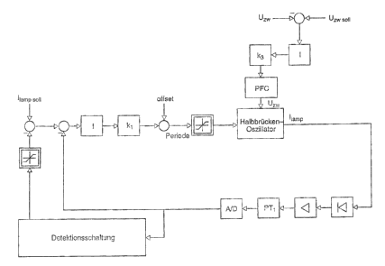
Figure 1 shows a scr:e:matic illustration of operating
equipment according to the inVention~
Figure 2a shows, schematioally, the re:Lationship
between the intermediate circuit vol-t:age, the discharge
lamp current and the qualitative current wa.veform in
switching elements of an oscillator circuit in an
operating circuit acco~~ding to the inzre:.v~..on;
Figure 2b corresponds to Figure 2a, but _relates to an
operating state closer to resonance; and
Figure 3 shows a block diagram of a program sequence in
a control circ-ai t in the o:oerat-~-ng circuit shown in
Figure 1~
~c~~t mod. ~'~~ c~.~~°~r~xa~ cs~.~ ~~~:~ ~~a~~r~t~~xz
3 :~
In Figure 1, the reference number 1 denotes a low-
pressure discharge lamp with two incandescenl~ filament
electrodes 2 and 3m A half--bridge oscillator circuit
wi,~.h two switching transistors 6 and 7Y which is known
CA 02431666 2003-06-10
- 10 -
per se, is connected beet>~een a ground connection 4 and.
an intermediate circuit supply voyage 5e The twc
switching transistors o and 7 can be switched
alternately in order to switch a oenter tap 8 between
the intermediate circuit supply voltage and t:he ground
potential. A radio-frequency supply voltage for the
discharge lamp 1 can thus be produced from the
rectified intermediate circuit supply vol-Rage, which is
applied to the connection 5 and is obtainE:d from. a
ma;-ns voltage via a rectv~fier bridge circu;~t, which is
known per se, wi'~h a PFC circuit
The PFC circuit, wThich is not shown in Figure 1, may be
a so-called step-up control~_er whose design is lcnown
per se andis not of interest in detail for the
i nvention It may also :oe any other PFC circuit
o s
Despite thePFC circuit, however, a certain amount of
residual modulation intermedi~;_t~e c;_rcuit
v~emains
cn
the
voltage at twice the mai ns freque ncy, that is to say
normally at 100 Hzo
A so-ca--lied coupling capacitor 9, a. lamp inductor 10
and the discharge lamp 1 are connected in series
between the ground connection 4 and the center tap 80
The coupling capacitor 9 is used for decoupling the
dischara~e lamp 1 from DC componentsg the lama inductor
10 is used in particular to compensate for the
dissipation, which in some eases iu; negativre, o:E the
cu_rrent/voltage characteristic of the d,_scharc~e _i_amp 1e
These func~icns of these two circuit components are
generally known and, there=ore do not need to be
explained in any more detail here.
The same is true for a resonant capacitor 11. whi c'm is
3.5 connected in parallel ~.ai-th the discharge lamp 1 and is
likewise connected in series w;-tl~ the coupling
capacitor ~ and -the lamp inductor 10, and which is used
to produce starring voltage ampli'~~udes increased by
resonance, for s'~artina :he discharge lamp ~.
CA 02431666 2003-06-10
- 1 1 -
To the extent that it ha.s been described so far., the
operating circuits design is completeln conventional.
f_owever, tYie control con nections of the switching
transistors 6 and 7, as i ndicated by dashed lines in
Figure 1, are controlled by control signa,~s from a
digital control c=~rcuit ~-2. The digital control circuit
12 is a programmable rn icrocontro~.lev and uses a.
measu-cement resis~~or 13 to detect a signal whic=a
indicates the magnitude of the current th_~ough the lamp
inductor 10.
In particular, the cone-rol circuit l2 contains a
current regulation ci-cult, which regulates the lamp
current that is upped o=f via the resistor 13 at a
largely constant value I.~ar,~. The mete.~~r~d o:C operai_ion of
the control circ~,:it 12 is shown in more detail i-n
Figure 3.
The control circuit 12 can thus measure the lamp
cu rent ILamp through the r~leasu-rement: z:esisto.r 13,, and
furthermore uses tile operating frequency of the half-
bridge oscillator together with t:~e switching
transistors 6 and % to regulate a constant lamp current
and, finally, is able by evaluating the remaining-
modulation of the lamp c.r-rer.-t amplit:ade resulting from
the modulat~'ion of the intermediate ci--cu.it voltage to
identify operation that is too close to ;lapac.iti ve
operation. As is expia.-fined with reference to Figure 3,
this is done using a threshold val~~.e for the
difference, as illusi~~~ated in Figures 2a arid 2b,
between the lamp cu_rren~~ amplitude maximmm I",w and the
minimum Im=;..
F figures 2a and 2b show schematically tree qualm-native
form of said f,-uCtuat:Lons for an operating state as
illustrated in Figure 2a, which is close to resonance
but is advantageous, and for Gn operating s~.Gte as
illustrated in Figure 2b, ~.,,~nich is disadvantageous m
CA 02431666 2003-06-10
- 12 -
This shows t_~e change in the magnitude of the
fluctuations of the lamp cu.r_ren~~ Ii,,mp that is tapped
off across the resister 13, and the corresponding
changes in the intermediate ci rcuit ooltage U2K that is
produced between the point 5 and the ground connection
4. The lamp current is shown with its envelope, which
illustrates the fluctuations in the amplitude: ~ait:n the
intermediate circuit voltage UZw. In fact, the lamp
current ILamp OSC111ateS at the operating frequency of
the half-bridge csciilat~o_r circuit, as is indicated
only schematically in Figures 2a and 2b.
The lower area of each of the figures shows qualitative
current waveforms of t:he '-calf-period currents flowing
through the respectively closed switching transistor 6
or 7. The limited negative dE>flection w'r~ich can be seen
initially in the left-hand current waVeforr~ in. each
case is typical for inductive operation and means that
the current is lagging the voltage. A~ long as the
negative peak is not too pronounced, this may be
regarded as an advantageous operating state. ''he right-
hand current waveform in Figure 2a shows ~ha~L the
negative deflection which indicates inductive operation
has virtually disappeared in the area of the small
amplitudes of the lamp current, that is to say in the
area of the minimum intermediate ci i:cuit voltages Llzw.
The proximity to capacitive operation thus fluctuates
with the intermediate circuit voltage U~~,,. In a
corresponding ma_rlner, the r:~ght-hand current: wa.veforrn
3G in figure 2b shows a pronounced positive peak at the
start of the current waveform, which symbc>lizes the
onset of capaci~ive operation. This peak leads to
thermal leads and possibly to damage to the switching
transistors 6 and 7, and srvould be avoided.
Figure 3 uses a block diagwam to show the method of
operation of the operat_ng circuit from Figure 1. The
illustrated procedure is run in the form o:E software
that is stored ven the microcontroller 12. According to
CA 02431666 2003-06-10
- 13 -
the upper end of the bloclc di~.gram, a measured
intermediate circuit voltage (betwee:~ the points 4 and
in Figure 1) UZ~.,, is subtractec. from a nominal
intermediate value «oltage U~wnom~ ''~he di'f~°r_e.~ce is
5 integrated by means of_ an integration element that is
symbolized by I; z_s multiplied by a normalization
constant that is deno~~ed k3, and i:> used to regu~~~ate
the PFC circuit ;;~ahi c:h ;-s not shown in Figure 1) to a
constant output voltage~ For this purpose, the
switching processes of the scaitching t-ransist.or of one
swi tching transistor in the ?FC circ~_i t, fo~~ example a
step-up controller, are c__ocked in an approrriate
manner, that is to say, in the e:nd, the operating
frequency of the stlritching transistor is varied such
that the output voltage arvd hence the intermediate
circuit voltage U~w are as constant a.~=_~ possible a 'the PFC
circuit outputs this ~_.ntermEadiate circuit voltage via
the points 4 and 5 in Figure 1 t:o the half-bridge
oscillator, which is formed by the switching
transistors 6 and ?, and the load circuit which
contains the lamp 1.
The half-bridge oscillator with ti2e switching
transistors 6 a~~d 7 produces the lamp current ILGTn~
which flows th_rovagh the lame; and is measured across
1
the measurement ~~~esistor 13 by the rnicrocontroller 12
n
This is symbolized by the arr ow which emerges to the
right from the half-bridge osc illator in Figure 3o The
lamp current is -rectified. and amplified in the
microcontroller b~~ means o== the elements w_~~ich are
denoted by the appropriate elect_r;~cai encineering
circuit symbols, is then f iltere:in a low-pass
element, which is deno;~ed by PTl, in t:n~e sense o-
forming a mean val ue, and is fina..l_~yr convE:rted
from
analog to digital form.
This is followed, by a bran<,h, whici~ on the one hand
leads to a block which is referred to as a detection
circuit. This detection ci-~~cait calcuiate~ the
CA 02431666 2003-06-10
- 14 -
fluctuations in the l.ar~p current amplitude over a time
period of 10 r<.illiseconds, that is to say the
difference between the maximum a~~d ~.he minimum of the
lamp current amwlitude and the envelope within said
time period. If this dz_fference is greater than a v alue
of, for example, 50 mA, the detection circuit incre ases
its output signal, otherwise it reduces it. Tre
detection circui t thewNew:ore assumet~ ~~hat, in normal
circumstances, no output signal is necessary, and its
output signal is thus 0 i:z these normal circumsta nces
(and cannot be reduced any furthe_ either;. I=~ the
threshold value of 50 mA ,ws exceeded, the output si gnal
is increased. by a specific fixed va'_ue and, once the
10 ms time peri od has <~1_ap:~ed, is increased by this
fixed amount once again for as long as the 50 m1~
threshold value is exceeded.
As soon as the threshold value is n.o longer exceeded;
the output signa-1 is reduced in steps, with a smaller
s tep width pre f era:oly being used thar,~ for increase
the .
This continues do~ln to an output si anal of 0, provided
that the threshold value for the iamx7 current
fluctuations has not :been exceeded again du ring this
period. The detection circuit thus i.Ases the threshold
value to identify excessive proxircu_ty to capaci
dive
operation, -reacts with an output signal to this
detection, and s~-cwl_y decreases the output signal
a.,s
soon as this detection no loraer occurs.
The described output sic~inal is limited with regard to
feasible measurement errors and is th:.en subtracted from
a lamp current nominal vulvae IL~,m~ nom in the subtraction
element, which is symboliz:=d by a minus sign. r~he
actual value of the lamp current IL~,.~,;~, averaged by the
digital averaging element, =:s v_n turn subtracted from
this corrected lamp current nominal wa_luen The
difference between hem is integrated, and is
multiplied by the n~~r:~raliration constant, that is
symbolized by k1. The integrated and normalized
CA 02431666 2003-06-10
- 15 -
difference between the lamp current r_omina~_ value as
corrected by the detection- circuit and the larnp current
actual value is ti~en added, in the element symbolized
by a circle and in accordance wi-~~h -~:ne arrow annotated
offset, to a va 1 ue in ovc_er to adj ust the operat i hg
pointo This value once again represents a. per;~od
duration limited with respect to feasiole measurement
errors, and is used for drivimg the swi~ohing
transistors 6 and 7 ,-n the half-br;~dge oscillator.
IC
Thus, overall, it can be s eE:n that the PFC c:ircui'~ is
firs t of ali regulated at a constar_t inv~ermediat.e
ci rcuit voltage with a nominal value UzW,,oI~,. The
intermediate circuit voltage modulation which is passed
i5 through by the PFC circuit influences v~he lamp current
via the half-bridge oscillator, wlth the l amp current
being regwlated by a second control -loop at a lamp
current nominal value ILamuNO~,,~ This is done using a
simple, slow I control loop, because only long-term
20 drift effects need be taken into account. This lamp
current nominal value is in turn corrected by a_ third
cont-.~ol loop, in which the detection c-_rcuit is
connected, such that the threshold value of 50 mA for
the lamp current amplitude modulations is note exceeded
25 all the time.
It can also be seen teat, in addition to the lamp
current regulation which is provided in any case-, the
invention has on,_y one further sloe control loop in the
3Q sense of ar_ additional_ software bra.nc h, fo_r wh-ch no
further determination of measured values is necessaryo
In fact, the lamp cur_-~ent. which ,-s mea:~ured and
digitized ;~.n any case is used.
35 If necessary, the described regulation process can be
supplemented by a further _regu7_ati on element in the
lamp current con'~.rol loop, in order ~o attE:nuate the
100 Hz modulator on the lamp current. By way of
example, a PI regulator could be used instead of a
CA 02431666 2003-06-10
- ,~~ -
simple I regulator. Th;_s changes nothing, even if
relatively small -lamp current modulations remain. Even
if the lamp current modulations were to be smoothed out
completely' they could still to this extent be used for
the detection according to the invention cf ~~.he
proximity to capaciti~re apera.t;-on, as the actuating
signal for the lamp current control ~oop~ representing
the fluctuations in tr.e lamp currentz The fluctuations
in the lamp current would then to a certain extent
exist only from the control engineering point of view
and ~.aould no longe_r_ actually be whysical -1y present. The
invention. also relates t o this variant. In facts even
with perfect lamp current regul anon, the cur:=ent would.
enter the capacitive area.
Apart from. this, it has already been stated that the
intermediate circuit voltage U~t~ in Figure 2 and that
between the cennec'~ion 5 and ground ~'a --n Figure 1 could
also be a delibera'~ely modulated voltage from a DC
voltage sources This would change nothing w~_th _regard
to the principle of this exemplary embodiment. However,
the PFC circuit would be superfluous i.n tr~.is ease.
The inventi on thus allows qu-~ve precz_se matching of the
operating circuit to cont~.nuous ope-_ration ~',iat on
average is close to resonance, v~ith lit'~le ad.diti onal
comp-~exity and despite-: component to_Lerances and -'amp
aging processes. In contrast to the prior art, lamp
operation continues ,.~rhen d;-fficL.ltie~> occur a_~d changes
in the current nominal value result only in a certain
reduction in power . =~ rem the user' s pevspect~i ve, this
represents a far better solution with a lamp whose
brightness ;-s decreased to a scarcely pe-~cer~t;_ble
extent in comparison to a lamp which does not obe=rate.