Note: Descriptions are shown in the official language in which they were submitted.
CA 02431819 2003-06-11
TITLE OF THE INVENTION
Thermal Electric Energy Converter
~~IAI~E OF THE INVENT01'~
Quentin Elias Diduch
FIELD OF THE INVENTIO=N
Ol This invention relates '°electrom.agnoti~; to electric" energy
conversion for energy
generation, thermal cooling, and electromagnetic signal reception,
particularly in the
thermal energy range.
I3ACI~GIZOUND OF THE It~IeIENTION
02 Ambient thermal energy and. electromagnetic energy tends to cause noise in
circuits and also limits operating points of electronic devices. ~~ his is
undesirable as it
reduces the functionality of the devices. As well there are many uses for
devices that can
convert a modulated electromagnetic sigrai back into a dec: odable electrical
signal. Thus
it is desirable to have a device that responds to thermal radiation and can
convert it back
into electrical energy or electrical signals, particularly when the
electromagnetic energy is
in the infrared energy spectrum. Current thermal energy 1:~; electrical energy
conversion
devices that exist are either temperature measurement devices or lov4~
efficiency detection
devices. These devices include thermocouples that produce energy when there is
a
difference of temperature acr oss the device, and a thermal diode structure
that is used for
signal detection.
03 Hc~~vever, these devices all suf fer at least ono of the following
disadvantages: ( 1 )
The inability to have dramatic cutoffs to frequency of operation, (2) the
requirement of a
temperature difference for operation.. (:l) the necessity of an external
voltage source to
bias the device, (4) the inability to act as a power source, (5) the inability
to act as a
cooling device, and (~) ambient energy recovery capabilities are lirr,~ited or
are non-
existent.
CA 02431819 2003-06-11
2
04 ~ther methods of solving tln: cooling problem are often implemented by
providing a way to rapidly draw away the thermal energy tom the circuit by
using
cooL~ng fans, or other cooling struetures. This solution has the distinct
disadvantage of
co,;nplete energy Ioss without any recovery of the dissipated energy.
OS This invention combines the characteristics of ~naveguides and rectifiers
to
convert electromagnetic energy to electrical energy. It is well known that
electromagnetic
waves traveling down a waveguide s-trLicture induce fields into the surface of
the guide,
and that these fields in turn can induce currents in the guide if it is a
conductor. T he field
patterns produced in the guide arc well descrilsed using Maxwell's field
equations. one
can solve these patterns such that the maximum and minimum field values for a
given
frequency and given mode of operation are known, as shc,~rn ire fig. 5. In
Fig. 6, the
waveguide 60 has a field induced upon its surface, the field represented by
lines with
arrev~~heads indicating the polarity. The scale in radians along the z
direction is
normalized with respect to an arbitra~°y wavelength. Rectifying
material characteristics
are well Icnov~m for their ability to limit current flow to one: direction.
I3y combining the
characteristics of these two devices we en d up yrrith a device that converts
high frequency
electromagnetic energy into electrical energy.
~~JMM~RY OF TH1J IN~IE~1TI~~I
06 This invention combines the characteristics of an electromagnetic waveguide
and
the characteristics of rectifying materials to convert electromagnetic energy
into electrical
energy. This is achieved in one embodiment by creating the guide structure
geometry
such that it is made from rectifying layers with the center of the guide
filled with a
material of a higher index of refraction than tl~e materials composing the
rectifier. The
rectifier is oriented such that the device is peryendicular to the path of'
maximum field
potentials such as those shown in Fig. ~. This guide can be further modified
such that its
ends are closed off, or partially closed off such that it forms a resonant
cavity, without
loss of functionality, as shov~Tn, for example, in I~ig. 5.
CA 02431819 2003-06-11
J
07 By placing the rectifier material in th.e path of max imu m potential of
the guide, it
forces the electromagnetic energy that enters into the guide to be reduced in
amplitude as
the rectifier alters it. The energy clipped by the rectification process is
novr electrical
energy. However, this electrical energy is a high vfrequency half wave pulse
and will
rapidly decay back to thermal energy if it remains as such. The attenuation of
this signal,
using standard methods, can typically be described by:
where t~, fit, ~ are the angular frequency, permeability, and oonduotivityr,
respectively.
Using this approximation, we realize that for wavelengths in the order of ten
rr~icrometors
(infrared radiation} the distance is typically on the order o1' a wavelength
before most of
the energy is transfoi-rned back into electromagnetic radiation. ~Ience it is
necessary to
change this pulse into a lower frequency form of energy.
08 ~ne method of achieving this is to connect several of these guiding
structures in
parallel such that pulses are slightly out of phase. By doing this one
effectively creates a
noisy I7C power source or a l~C pulse ~~nodulated signal source as shcawn in
Pigs. ~(a),
(b}, and (c), provided that all the guide structures receive electromagnetic
energy in the
frequency range that they were designed for. Pig. 3(a) shows the input
~vaveform as
induced on the ~.vaveguide, Pig. 3(b} shoves the waveform after rectification,
and 3(c}
shows approximately the results of combining multiple rectified waveforms in
parallel.
09 The shape of the guiding structure may be any stars ~~~ard guide shape
provided that
the maximum and minimmn potential points can be deterts2ined along the guide
for the
frequency range in question. The design preferably allow; for the maximum
amount of
field interaction with the rectifying material to induce maximum voltages into
the
material. Hence the positioning of the rectifying structure depends upon the
guide
design. In a preferred embodiment, the rectifying structures compose the
inside surface
of the guide and are preferably aligned t~ the direction of sarface current
flo~dv, or across
regions of field potential maxima and minima. The frequency range oi:
operation of the
device is dependent upon several factors including the dimensions of the
guide, the
difference of index of refraction between the gL~ide and the material that
fills she guide, as
CA 02431819 2003-06-11
well as the location of the rectifying material, the maximum frequency of the
rectifiers,
and of course the geometry of the wavegui'.~e itaelf.
The rectifier material is preferably treated such that it has low to no
threshold
voltage and a high frequency response, as it may have to respond to Z'fIz
range
frequencies (application dependent). Also the rectifying device is preferred
to have a
high conductivity.
11 This device and its design metl°~odology are appropriate for vse as
an energy
conversion device, energy recovery device, cooling mechanism, thermal sensor,
infrared
sensor, or high frequency antenna.
12 There is therefore provided according to an aspect oR~ the invention a
con~jerter for
converting electromagnetic energy to °lectric energy, the converter
corr~prisir~g a material
transparent to the electromagnetic energy with an index of refraction
surrc~anded by a
material with a lower index of refractioif, the j:~-o materials forming a
wavoguido, and ~
rectifier coupled to the waveguide and positioned to rectify the
electromagnetic energy
and form a positive and a negative region on tl~~ converter; from whiol~ a
currant may be
drawn. The rectifier may be constructed with the surrounding material of the
waveguide
having alternating layers oz p-type and n-type gnaterial, which may be
separated by
intrinsically neutral material. The rectifier rnay also ~o~r~priso a ballistic
rectifying
structure, v~hich may be formed on th-a inside of the surrounding material.
several
converters may be incorporated in a cluster connected by oonducti~~re
connectors or
electronic components, and may be enclosed in an electromagnetic cavity, which
may be
comprised of black silicon.
1312IEF I3E~CIZIPT'ION OF'f~IE FICIJP~E~
13 Preferred embodiments of the invention ~~ill now be described with
reference to
the figures by way of example where like characters denote like element; and
in which:
Fig. 1 is a single waveguide with 2 sides of the guide surfaces oo~rnposcd of
bridge
rectifiers, the image to the right shows a zoomed image of the ballistic
rectifier structures.
CA 02431819 2003-06-11
Fig. 1 (a} is a schematic of the ballistic rectifiers coupled to the
wavegt~ido.
Fig. 2(a) depicts the cross section of the TFIz speed Schottky diode
structure.
Fig. 2(b) shows a ballistic bridge rectifier
Fig. 2(c) is the front view of z reduced scale ballistic rectifier composed of
inCraAs and InP.
Fig. 3(a) shows a typical electromagnetic input wav~;for~~n of arbitrary
Frequen~;y.
Fig. 3(b) shows the resultant ~~aveform after it has been converted from
electromagnetic radiation into electrical energy.
Fig. 3(c} shows the resultant wraveforms when an unequal length interconnects
are
used to connect 4 devices together.
Fig. 4(a) is a typical node configuration connecting 4 ballistic bridge
rectifier
based devices together with semi-equal length runners.
Fig. 4(b) is a typical configuration connecting 4 PN based devices together
with
semi-equal length runners.
Fig. 5 is a partial crass section of ~ devices encased in a black silicon
cavity, with
a possible path for incoming radiation being demonstrated.
Fig. 6 is a diagram of surface currents that dominate guide operation without
rectifying materials in use.
Fig. 7 is a circuit diagram of a set of waveguide based converters connected
to a
load.
Fig. ~ is a single waveguide in a laterally striped rectangular configuration
composed of PN material.
Fig. 9 is a single waveguide in a longitudinally striped rectangular conf
guration
composed of PN material.
Fig. I O shows the frequency distribution of a black body at 300K source.
Fig. 11 shows the power potential as a function of ter.~peratu:re and
f~°equency
range.
DETAILED DESCRIP'hI(~N ~3F PREFERRED EMBDDINIENTS
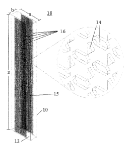
14 A preferred embodiment of the invention is shown i:n Fig. l, where a
converter 1 ~
is fabricated by etching waveguide structures of a given width and t:riickness
into an
CA 02431819 2003-06-11
6
InCiaAs substrate and doped such th~.t a quantum well composed of In~~aAs-InP
enables
the formation of ballistic bridge rectifier structures IS within the confines
of the guide.
The rectifier structures 1 S are coupled to the waveguide by being
forma°.d on the inside of
the outer layer. The waveguide is generally composed of an outer layer 10 of a
higher
index of refraction than the inner mater-.°=al 12. The ballistic bridge
rectifiers are shown in
more detail in Fig. 1 (a), in which I4 denotes regions that have been etched
away, and in
which the rectifiers are connected in series. Tie ballistic bridge rectifier
structures have
conductive contacts, such as metal contacts, that interconnect the ballistic
bridge
rectifiers, interconnect waveguides, anti act as output col~aacts. In Fig. 1,
tl~e metal
contacts I6 connecting the ballistic bridge rectifiers are shown, while the
metal contacts
interconnecting waveguides and acting as output contacts can 'be seen in Fig.
4{a). In this
figure, the series of rectifiers are cor~nect~d in parallel at each edge of
the guide using
metal connections I 6. 'these connections are then interconnected to adj scent
guides by
implementing metal contact pads 40 and metal interconnects 42. Fig. 1 shows a
rectangular guide with an internal width a, an internal height b and a depth z
such that
a>b. According to a preferred embodiment, the following ca~~ be used to define
the
dimensions of the waveguide structlue: a > ~,/2 is required in order for
energy to be
allowed into the waveguide, where a ~ 3b.
15 As an example, we ~~i11 consider a black body at IOU I~, which has a
frequency
distribution as shown in Fig. I0, where the vertical axis has units of watts
per meter
squared ('V~/m~), and the horizontal axis is frequency {I~z). Frown the
frequency
distribution we observe that that majority of t:he energy is centered at
around 1F to 20
Tllz. 'Thus the currents on th.e surface of the °~raveguide will be in
about this frequency
range. Utilizing the cutoff frequency of the guide one can eliminate the lower
frequencies. Thus, it is possible to create a reasonably coherent
electxomagnetic energy
source. In Fig. I I we show the power distribution over the wavelengths of I ~
microns to
I ~.?5 microns (along the front of the graph), ~rhich correspond to 20 and 16
~I I-iz,
respectively, and over a terraperature range o:: 100K to ~i00K {side axis).
The power
output on the left of the chart is in fVatts per square meter, per wavelength
{in meters).
This provides us with the magnitude of energy available for conversion as
temperature
CA 02431819 2003-06-11
7
changes. The area (not volume) underneath the curve at any one temperature is
the
amount of energy that can be extra.c;ted at that temperatL~re. This e~;ample
assumes a
bandwidth of operation of 4 TIIz; which still leaves the signal reasonably
coherent. This
bandwidth can be increased with raster rectifiers. Caive~ that thc~
electromagnetic
radiation within the structure is between l6Tflz to 2~THz, we can assume that
every 15
to I x.75 ~m a new ~~ave front exists. Random phase noise at the input doesn't
pose a
problem, as all the voltages end up half wave rectified to I3C, .producing a
pulsed L~C
current in which the LjC pulses sum togefher. ~Jnlil~e with AC current; where
additional
energy can remove potential, the current can o~~ly increase with IBC.
16 Solving for the size of the ope:ciing of the guide using:
.fre~o = ~ l(~C~ ~~ ) (~)
16 Tliz = c/(2a)
gives: a . 3.4 lEm
Thus, for power generation in our examples a is 9.4 Vim, and b is ~ ~rr~
according to the
1 /3 rule presented above.
17 In order to generate 1~C pulses with incident infrared light, we require a
rectifier
that can operate in the TI~z frequency range, and in our example, up to
approximately 2D
TI~z. A preferred rectifying scheme utilizing ballistic rectifiers is shovrn
schematically in
~'ig. 2(b). These devices have a very high frequency response, and virti.~ally
no threshold
voltage. ~ low threshold is highly advantageous as it enables a larger
percentage of the
incoming energy to be fully rectified. ~Jhile faster devices enable more power
extraction, realization of this invention with devices that operate in the low
Tflz region is
possible. The ballistic rectifier is based upon the ballistic; electron
effect, where device
feature size is small in relation to the rr~ean free path of electrons. Thus
elect~~ons that
encounter obstacles behave in a more or less I~Tew-tor~ian manner. This
implies electrons
travel in straight paths rather than in a drift manner, and, thus we can use
deflective
structures to create changes in current paths. The dark areas 14 in Rigs. 2(b)
and (c) are
regions that were etched away, so as to cause de~actions in the path of the
electrons.
Deferring to hig. 2(b), an ~C source across points S and 1=3 causes ballistic
electron
CA 02431819 2003-06-11
g
motion, and the electrons will be deflected toward f, as depicted in the
figure. Since the
electrons are deflected toward i., this Ieaves region rJ d~I:~lct~d of
electrons. 'thus one
sees that this type of structure functions as a bridge rectifier. The
efficiency of this
device is directly proportional to the mean free path of the material, so in
general the
rectifier functions better at Iower temperat~~res. however, as long as the
mean free path
is larger than half the size of the triangular strLacture, the device still
functions. Fig. 2(c)
is another ballistic bridge rectifier that acts similar to the one slZOVVn in
Fig. ~~b), where
the paths of the electrons are denoted e, and the electrons are also deflected
by the etched
area 14. These rectifiers can be fabricated on the inside ~~~~ the higher
index material in
the waveguide to form an energy converter. A more detailed description of the
formation
of the ballistic rectifiers as described above can be Iound ~n
°°~peration of lnt~aAsIInh-
Based Ballistic Rectifiers at Room 'Temperature and Frequencies up to SOGI~z"
A. ~I.
Song, P. Omlin.g, L. Samuelson, VV. Sei ~.r~, I. Shorubalko, ~. ?irath, .Ipn.
J. Appl. Phys.
Vol. 40, Pt. 2, I'~o. 9A/B, 2001.
I ~ There will nov; be described an example of~ the fabrication of a device to
operate
in the frequency range of our example. The fabrication of the wave-guide
structure stars
from a InC3aAs substrate that is first etchec'L to create a wolf structure
that is I00 microns
long by 9.4 microns wide by 3 microns deep, corresponding to dimensions a, b,
z in Fig.
1. This structure is then modulation doped such that a Iru~.~s~"ra~,25As/InP
quantum-wall
structure is created. The properties of this structure ar~;; such that the
electrons are
confined to a two-dimensional electron gas in a 3 nrr~ thick quantum u-~ell,
located 40 nm
below the surface. The rectifiers are defined using electron beam lithography
and wet
chemical etching. In Figs. ~~b) and 2(c), the dark areas 14 are etched a~Jay,
to create the
rectifying layer 1 ~ of Fig. 1 on the inside surface. The cavity left by tl~e
etching is then
filled with Si02, and an Aluminum metal Iayer is placed over top of the
structure creating
a guide structure. The two ends of the guide arc left open for energy to flow
through the
structure. 1~1-ote that only one side of the waveguide has the r ectifiers
etched info it, which
is an alternative to both sides in order to simplify fabrication.
CA 02431819 2003-06-11
9
19 Schottky-type rectifying device developed by Karl M. Strohm et al. can also
be
used as an alternative to the ballistic rectifying scheme described above.
'Those devices
have achieved a 1 '~'I--iz frequency limit using a silicon process in 1998. A
cross section
of a p-type diode is shown schematically in Fig. 2(a). ~'h~: device is on a
highly .resistive
silicon substrate 20, with a heavily doped p~ region. On this region are tvvo
ohmic
contacts 24, separated by a layered structure consisting of a lightly doped p-
epitaxial
layer p, a schottky contact 22, and an Au layer on top. The fabrication
procedure is
described in detail in Stroh~n et al, "S~VI~VI(JC Rectenalas on Nigh-
F~esistivity Silicon
and CIIVIOS Compatibility", IEEE Tran sections on Microwave Theory and
'fechnidues,
VoI. 46, No. 5, May 1998. The Schottky str~xctures are formed like the P=1~
structures
shov~m in Figs. 8 and 9 by substituting metal for the 1~1 structure.
20 Another alternate rectifying scheme for the energy conversion device is
fabricated
by etching waveguido structures into a silicon substrate sus~h that layers of
P material and
I~T material of a given width and tr~iclcness are created within the confines
of the guide, as
shown in Fig. 8, where the converter is labeled 80, the layered outer material
is labeled
82, and the inside of tree vaaveguide is labeled 84. With this rectifying
scheme, the
rectifier no longer consists of the inside of the outer layer, rout rather
oor~sists of the entire
outside layer. The result is a series of pN junctions that act as rectifying
diodes to the
surface currents. There is preferably an even number of layers and the bottom
and top
layers ha~~e conductive contacts, such as metal contacts, used to interconnect
the
individual guides as well as for output contacts. In the near infrared that we
are
considering, the guide structure 3nay be '~illod with Si02 to enable the
g~~ide functionality,
however, any substance with the appropriate transparency and index of
refraction in the
desired frequency range would be appropriate. For a rectangular guide; withF
an internal
width a, an internal height b such that a >'n, and a depth z, the following
equation defines
the center of the locations of the PN lay ors:
CA 02431819 2003-06-11
to
where k is odd for 1' material and ev~~~ for N material, and ~ is the
wavelength. Note that
a > ~ is required in order for the guide to ;allow energy into the guide, and
that the
thickness of each layer must not exceed ~ n to prevent the l~ and N materials
from
overlapping. t~lso note that there must be ~. minimum of 2 layers for this
device to
function (a p and an N layer). The wavegmides ~0 can be ~;onn~cted as shown in
fig. 4(b)
v~~i~.h rneta~. contact pads 40 to the positive and ~r~,gative terrr~inals,
and metal interconnects
42 for interconnecting the individLaal wave~uidPs ~0.
21 Alternatively, p'ig. 9 gives an example of a more frequency independent
solution
to the idea of using 1' and N materials. ~,h~; outer material 9~ that covers
the inner
material of the ~w~aveguide 94 can also be layered along its height or width
to form a
converter q0, instead of being layered along its depth as in rig. ~. In dig.
9, a layer of h
and of N are made to form a waveguide, tlae layers being along the width of
the
waveguide, but the layers could also be along its height. The layers are
constructed such
that 1-d of a is P material, and d of a is N material, such that d < 1- 2~ ,
where T is the
minimum thickness that the N ~~nateriai can be, and leas been normalized with
respect to a.
These materials preferably run the full height (or width) of the guide ~.s
well as the full
depth. 'This creates a rectifying diode structm°t~ along the width or
height, as opposed to
the depth discussed before. Increasing the depth of the structure increases
the e~frciency
of ti~P guide by allowing more energy to be extracted from the electromagnetic
radiation
as i.t interacts more with the rectifier. 'The structure should have a depth
or' at least 1
wavelength.
22 The process by which the electrical energy is e~traoted from ballistic
bridge
reo~tifiers and ~N structures or schottlcy structures is somewhat different.
ballistic
rectifiers add up like several batteries in aerie s such that '~h~: current
does trot increase
while: the voltage increases. ~.lso, the size of the rectifier is much smaller
than the
wavelength of the radiation. 'l'hus the su~a~rr~ation of the energy at the
encl of each rectifier
string effectively adds up slightly out of phase sine the ve;locity° of
electrons is less than
CA 02431819 2003-06-11
the speed of light. fence ono wave-ga~ido structure composed in this
me°.thodology should
be sufficient to produce power, provided that the length of th o guide is
large in relation to
the wave-length, which would be approximately 1.5 times. as long, given the
differences
in speed. ''his is not the case with the pl~V junction versions, as the hIV
Junction or
Schottky structures essentially act as one rove of ballistic devices. 'f he
ballistic devices
are bridge rectifiers and not cl.iodes in forms of ehavior.
~3 ~ther rectification structures nay be used. ~'or example, the layered 1N
structure
can be extended to include an intrinsic layer; forming a layered hIIV
structure. As with
the hl~I structure, a minimu~~n of I layer each must be present (for a t=otal
of 3 layers).
Also, high-speed schottky diodes can be fabricated on the inside of the
wavoguide in the
same configuration as the ballistic rectifiers to produce: the necessary
output signal.
ether schottky structures such as a p-~(etal device rnay also be used; as long
as the
frequency range is satisfied. ~'he 1'-lJletal device is a 1'-Hypo
semiconductor that has an
abrupt metal contact such that tine contact is not deeply en~;rained into tire
se~~~iconductor.
Ihis provides diode action similar to low a hldT diode functions, with the
exception that it
is now a heterostructure, and that the band gap energy prey.:nts holes from
moving across
the junction while electrons are able to arose the junction.
24 'a"he output signals from the guide structures are high frequency pulses,
(half wave
rectified signals of the original input signal, or ~'ull wave re~:tifiod in
the case of the bridge
rectifier). fence the waveguide structures have to be in very close proximity,
and
preferably within a distance of 1 wavelength. According '.o a preferred
embodiment of
the invention, the structures are arranged so tl~.at the connections are
clustered in such a
way that they are interconnected within a distance of '/~ o f a wavelength
such that any
wire carrying just a single 1~~ generated pulse is sho~rte~- than half a
wavelength.
~thorwise the majority of the onor-gy wii3 go back into thet-mal radiation. In
the case of
the ballistic bridge rectifiers, this means that any string connected in
series shouldn't be
more than one half a wavelength from the next string, or from an adjacent
guide (if
connected n parallel). Essentially, any location that generates a single pulse
per
electromagnetic wave that Boos by has to be within lZalf a wavelength of
another structure
CA 02431819 2003-06-11
that that could receive this ~.vave. Ficlds of one wave could cater multiple
guides, and
thus should be arranged. to add u:~. In operation, the output signal strength
is highly
attenuated and will lose approximately I/~ of its amplitude within a distance
of t/2 a
wavelength for near infrared frequencies.
25 ~y interconnecting tl~e guides v~~itl~ slightly out of phase distances,
such that
signals of similar amplitude are out of phase, one creates a lower frequency
pulse that can
effectively become a I7~ source, with a sufficient number of guides. then this
device is
designed for signal reception, the phasc-offset between de~,.-ices is
arrar~.ged such that the
signal is more in phase rather than offset in phase. In this case one lras to
consider
bandwidth limitations over signal strength, and signal propagating distances.
If the
interconnects are designed such that ~ guides are used to form a node as in
Fig. 4~a), each
should have an interconnect Length difference of 1/4. of a ~~lavelength vn
relation to each
other such that the output signal will effectively be a IBC pulse of 1
wavelength (see Fig.
~(cj). Fig 4(b) shows another cluster of converters, but this tune the
converters have a
layered PN structure. ~y preferably interconnecting these pulses so that they
are out of
phase at a common node point one is able to create lower frequency p1=.lses
that are able
to travel much longer distances. These interconnects do not have to be
conductive
metals, but could also be made up of other circuit elements common to the
Field that
would cause the pulses to be out of phase. 'hhis is to be continued until
either the desired
bandwidth/propagation distance requirements are met, or sLVCh that the signal
is a noisy)
~C source, if required.
26 ~Ihen these devices are used for signal reception, the design of these
interconnections describes ho~° the signal will be reconstructed fronu
electromagnetic
waves. For the most par's this can 'oe exactly the same as for power
gs;neration if
Amplitude Modulation is used or ii the mcsdulation is of low bandwidth. '~Jhat
is
important is that the length of the wires essentially dictates efficiency,
a:nd the shorter the
wires are the better. The slunrnation o-ø' phases leads to a coherent I;~C
source. If the
source is a random source and there are etzcug'.~ structures it docsn°t
matter l~ovv they are
setup as long as the lengths of wire are short enough so that tl~e energy can
sum together
CA 02431819 2003-06-11
ion the order of less than half a wavelength. if the source is a coherent
source, then the
structure should be structured so the lengths of wire cause tho energy to bo
phased
together. In this case, a serios of out of phase pulses are combined on to ono
wire so that
when together there is no space between pulses, i.e. C.
27 For power generation purposes it is preferred to surround tho guide c;r
cluster of
guides with an internally reflective cavity 5G. This cavity is prefera'oly
~;o~nposed of
black silicon for infrared radiation, as shown in Fig. 5, but other materials
could be
substituted by ono skilled in the art if the device was to opo~ato in the
optical ox other
region of the electromagnetic spectrum. i3laclc silicon naturally has a jagged
and peaked
structure, as shown in the figure, and the jaggod nature enables
electromagnetic radiation
to enter but prevents it from escaping bocause of the xet~aotion and
reflectnon effects
caused by air-silicon interface. Fig. ~ shows the electromagnetic radiation
F;~~I depicted
as a ray entering the cavity ~~, and being reflected internally along the
waveguide 52 as
well as inside the cavity, passing through the device 54 composed of P type
and N type
regions, denoted P and N respectively.
2~ Fig. 7 sho~-~s an example of now the energy converters 70 as described in
the
disclosure can be used as a power source. ~.s shown, they are connected ib~
parallel by
the metal interconnects 42 rArith all the positive contacts connected to the
node labeled
+ve, and all the negative contacts are connected to the ne~de labeled -ve,
however, any
arrangement that is commonly used to connect power sources can be used,
defending on
the desired application. 1~ load can thw be connected to +ve arid -~ve.
29 NtLdItiple waveguides need not be present for an application. Individual
wave-
guide can be used in different applications. As mentioned above, an individual
ballistic
design could function on its own as a power g~unerating device (albeit a very
how power
one). The other devices could be used as part of a reception system or even a
power
generation one; but the energy produced would be high frequency pulse
modulated.
CA 02431819 2003-06-11
30 Immaterial modiF°ications ~na~~ be made to the err~bodicnts sort for-
ard in this
disclosure by those skilled in the art ~r~~ithoa~t departing from the essence
of the in~~ention.