Note: Descriptions are shown in the official language in which they were submitted.
CA 02431914 2003-06-12
WO 02/060225 PCT/USO1/02036
ENERGY CONSERVATION
DIMMER DEVICE FOR
GASEOUS DISCHARGE DEVICES
Field of Invention
The present invention generally relates to energy conserving light dimmers.
More
particularly, this invention relates to dimmers suitable for high intensity
discharge (HID)
gaseous lamps.
Background of Invention
The development of arc discharge lighting, particularly high intensity
discharge
(HID) gaseous lamps, opened a new era in lighting technology based on the
improved
efficacy of low pressure sodium, high pressure sodium and metal halide bulbs.
H1D bulbs,
however, require a long time to warm up to achieve full light output. HID
bulbs are thus
maintained in an "on" state to avoid the long warm up time at the expense of
an increase in
the amount of consumed energy.
The increased use of fluorescent lamps in residential service and increasing
demand
for light level control resulted in the development of household type
fluorescent dimming
devices, which control the light level but do not efficiently conserve energy.
For example,
resistive dimmers are variable resistor devices that reduce the power to the
light bulb in
accordance to the ratio between the resistances. The overall power consumed
remains
essentially unchanged. Pulse Width Modulation dimmers are used predominantly
with
1
CA 02431914 2003-06-12
WO 02/060225 PCT/USO1/02036
fluorescent lighting. These dimmers have a better efficacy than standard
dimmers, but such
dimming devices are costly for both the replacement components and the
installation.
Capactive or liiductive phase shifting dimmers incorporate capactive or
inductive elements
in the circuit to introduce a phase shift in the electrical supply to the
light fixture. By
selectively switching, for example, capactive, components in and out of a
phase shift
dimmer circuit, the phase shift and corresponding power factor, of the input
voltage to the
light fixture are altered. These dimmers axe generally referred to as HI/LO
dimmers because
there is a high, i.e., full power, full illumination, position and a low,
i.e., half power, half
illumination, position. Variable autotransformers are another means of
reducing the voltage
to a light fixture by providing different input voltage levels. The different
voltage levels are
achieved by changing the position of a mechanical slide contacting one of a
plurality of taps
on the transformer. Variable auto transformers are constructed generally using
toroid or
linear transformers, which axe more expensive than laminated core rectangular
power
transformers.
The current technology of dimming devices has been developed primarily for
light
level control and not for efficient energy conservation. Thus, while the use
of gaseous
discharge devices is energy efficient and the illumination can be adjusted,
gaseous discharge
devices consume more energy than is necessary. Hence, there is a need for
dimming devices
that are able to control the level of illumination of gaseous discharge
devices and conserve
energy in a more efficient manner.
2
CA 02431914 2003-06-12
WO 02/060225 PCT/USO1/02036
Summary of Invention
The present invention discloses an apparatus to control the voltage and
current levels
supplied to a gaseous discharge device to dim the light output and to conserve
energy. In
accordance with the principles of the invention, a phase detector monitors the
phase angle
difference between the voltage and current applied to a gaseous discharge
device, i.e., load
side. When a request to alter the light output level of the discharge device
is made, a
controller circuit, in response to an indication of the load side
voltage/current phase
relationship and the requested alteration, causes a change in the supplied
voltage and
current. When the appropriated phase relationship is determined, the voltage
level is altered
in a manner such that the alterations occur in a time period, which prevents
the
extinguishing of the illuminating arc in a gaseous discharge device. Further,
the voltage is
prevented from falling below a minimum value needed to sustain the
illuminating arc in the
gaseous discharge device. In another aspect of the invention, the input
electrical supply is
provided directly to the light circuit to produce a maximum illumination
output if a failure is
determined to exist in the power dimmer circuit or if the voltage falls below
a minimum
level.
Brief Descriution of the Figures
The advantages and aspects of the present invention will be more fully
understood in
conjunction with the following detailed description and accompanying drawings,
wherein:
Figure 1 a illustrates a conventional gaseous discharge light fixture;
Figure 1b illustrates an exemplary electrical phase relation in a startup
condition of a
gaseous discharge light fixture;
3
CA 02431914 2003-06-12
WO 02/060225 PCT/USO1/02036
Figure lc illustrates an exemplary electrical phase relation in steady-state
condition
of a gaseous discharge light fixture;
Figure 2 illustrates a block diagram of an automatic dimmer system according
to a
preferred form of the present invention;
Figure 3 depicts a flow chart illustrating exemplary processing in accordance
with
the principles of the invention;
Figure 4a illustrates one embodiment of the present invention;
Figure 4b illustrates a simplified diagram of one embodiment of the present
invention;
Figure Sa illustrates an exemplary voltage zero-crossing phase detector;
Figures Sb and Sc illustrate an exemplary current zero-crossing phase
detector; and
Figure 6 illustrates an exemplary timing diagram of voltages applied to a
light fixture
in accordance with the principles of the invention.
It is to be understood that these drawings are solely for purposes of
illustrating the
concepts of the invention and are not intended as a definition of the limits
of the invention.
It will be appreciated that the same reference numerals, possibly supplemented
with
reference characters where appropriate, have been used throughout to identify
corresponding
parts.
Detailed Description of the Invention
Figure 1 a illustrates a conventional pulse width modulated dimmer circuit 100
controlling the voltage level of an input electrical source to light circuit
160, which is
composed of light emitting devices160, 162, 168, etc., such as gaseous
discharge devices.
4
CA 02431914 2003-06-12
WO 02/060225 PCT/USO1/02036
In this exemplary circuit, an alternating current (AC) electrical supply is
provided to fuses
110, which protect the circuit components from over-voltage conditions. Line
filter 115 and
transient protection 120 are used to smooth irregularities in the input line
voltage and aid in
preventing over-voltage spikes in the AC supply from being supplied to light
circuit 160.
The processed AC voltage is next applied to rectifier 125, which rectifies the
AC voltage.
The rectified AC voltage is next applied to filter 130 to smooth any ripple in
the rectified
AC voltage. The rectified AC voltage is then applied to Power Oscillator 135,
which
generates a high frequency AC voltage. The high frequency voltage is then
applied to
transformer 150 to step the voltage upward or downward depending on input
controls (not
shown). The secondary voltage of transformer 150 is then applied to light
circuit 160.
Although not shown, gaseous discharge devices, such as fluorescent and Hm
gaseous lamps, require ballast to operate properly. These devices produce an
illumination
when an arc discharge occurs through an excitable gas or vapor under
controlled conditions.
One of the characteristics of gaseous discharge lamps is that they operate
with negative
resistance. Thus, as operating current continues to flow, the negative
resistance would
enable the operating current to continuously increase until a lamp burns out.
To regulate the
flow of operating current, a positive impedance, typically resistive, device,
i.e., ballast, is
added to compensate for the negative resistance of the gaseous device. The
ballast
maintains the operating current at a substantially known level. A second
important function
of the ballast is to provide a voltage to the electrodes of the gaseous lamp
to initiate and
sustain the arc. Maintenance of an operating voltage across the gaseous arc
discharge device
is critical as the removal of the voltage for a time interval as short as
seven milliseconds can
extinguish the illumination produced by the light emanating device.
CA 02431914 2003-06-12
WO 02/060225 PCT/USO1/02036
Figure 1b illustrates the phase relation between voltage and current of a load-
side
electrical source during an initial startup, or warm-up, phase of the gaseous
discharge
devices in light circuit 160. In this case, the gaseous devices are
substantially inductive and
the phase of the voltage component 190 leads the phase of the current
component 180 in the
order of 90 degrees.
Figure lc illustrates the phase relation between voltage and current of an
electrical
source after the gaseous discharge devices in light circuit 160 have achieved
a steady state
condition. In this case, the discharge devices are substantially resistive and
the phases of the
voltage 190 and current 180 components remain within a narrow phase difference
195.
Further, in a steady-state condition, the phase difference between the
supplied voltage and
current remains substantially constant.
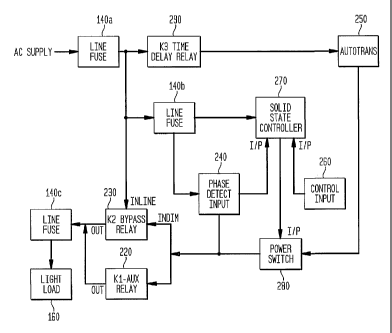
Figure 2 illustrates, in a simplified block diagram form, a light dimmer
switch in
accordance with the principles of the invention. In this simplified circuit an
AC power
source is applied to line fuse 140a, which provide protection from overvoltage
conditions.
The voltage, or power, which are used synonymously herein, is then applied to
by-pass
relay, or switch, 230, line-fuse 140b and time-delay relay 290. By-pass relay
230 provides a
direct connection of the input power supply to light circuit 160. This
application of full
voltage to the bulbs is important during the warm-up stage, as gaseous bulbs
require a long
time to generate, or strike, an arc that transverses the gaseous element
within the bulb. By-
pass relay 230 further provides for a fail-safe operation of the illustrated
circuit. In those
cases, when the dimmer circuit fails or unacceptable power conditions develop,
then by-pass
relay 230 is positioned to provide full input power to light circuit 160 to
prevent
extinguishing the HID bulbs. An optional indicator light (not shown) alerts
operating or
6
CA 02431914 2003-06-12
WO 02/060225 PCT/USO1/02036
maintenance personnel of this by-pass mode operation.
Line fuse 140b is representative of a line-in controller fuse that provides
overvoltage
protection for solid-state controller 270 and phase detector 240.
Time-delay relay, 290, provides a time delay to allow for a system powerup and
test
before voltage is applied through autotransformer 250 and power switch 280. In
a preferred
embodiment, a twenty-five (25) second time delay is nominally selected.
Phase detector 240 monitors the phase of the load-side AC signal during the
warm-
up stages and during normal operation. When it is detected that the phase
angle difference
between the input voltage and current exceeds a known value, then phase
detector 240
provides necessary indicator signals to restrict controller 270 and power
switch 280 from
changing tap settings. In a preferred form of the invention, the known
difference in phase
angle is measured as nominally 15 degrees.
Autotransformer 250 provides a plurality of discrete variable voltage values
between
a pre-determined high value and a pre-determined low value. The pre-determined
low
voltage level of autotransformer 250 corresponds to substantially a minimum
operating
voltage necessary to sustain the illumination of the HID lamps ~in light
fixture 160.
Solid state controller 270 controls the dimming process, indicates operating
conditions through optional visual display or audio alarms, and interfaces
with control
devices. Solid state controller 270 provides logical functions which control
the dimming
process by coordinating functions between components and interfaces with
control input
260, such as external sensors, infrared sensors, keyboards, keypads, variable
switches (not
shown).
Power. switch 280 maintains power between the AC supply and light circuit 160.
7
CA 02431914 2003-06-12
WO 02/060225 PCT/USO1/02036
Power switch 280 is composed of a plurality of semi-conductor switches, one
switch for
each of the plurality of taps in autotransformer 250.
In accordance with the principles of the invention, upon the application of
power, by-
pass relay 230 is initially operational to provide the full input voltage to
light circuit 160.
Phase detector 240 also initiates processes to analyze both the supply-side
power condition
and the load-side power condition. Controller 270 further positions auxiliary
relay 220 to
provide an electrical path through the dimmer circuit to light fixture 160.
When phase detector 240 determines that the phase relation between voltage and
current are within acceptable tolerance levels, an indicator is provided to
controller 270
which causes auxiliary relay 220 to close and provide the full input voltage
to light circuit
160 . Thus, both by-pass relay 230 and auxiliary relay 220 are connected in
parallel, and
each provides the a voltage level to light circuit 160. The system then checks
the voltage
output level and causes by-pass relay 230 to open. Thus, the voltage to light
fixture 160 is
smoothly transferred through auxiliary relay 220 and the dimmer circuit
controls the
electrical flow to light circuit 160 through by-pass relay 230 Auxiliary Relay
220 is
thereafter released.
When a light dimming request is detected, then phase detector 240 determines
whether the phases of voltage and current are within acceptable tolerance
limits and
provides an indicator to controller 270. Controller 270, responsive to the
indicator provided,
then progressively selects voltages from different tap settings of
autotransformer 250 until
the desired voltage setting is achieved.
However, when phase detector 240 determines an irregular condition in the
phases of
the electrical source, control of by-pass relay 230 is removed and tlae full
input voltage is
8
CA 02431914 2003-06-12
WO 02/060225 PCT/USO1/02036
applied to light circuit 160. Applying full voltage to light circuit 160 is
representative of a
default mode that provides a measure of safety. For example, an irregular
power condition
may be detected when at least one bulb is extinguished or burns out. In this
case, the phase
relation between the voltage and current is altered and rather than
maintaining a dimmed
light setting, the light setting is raised such that each of the remaining
bulbs is producing an
illumination at a designed maximum level. Optionally, an indicator or alarm
can also
indicate an irregularity has been detected.
Figure 3 depicts a flow chart of processing 300 to control the dimmer circuit
illustrated in Figure 2. At block 310, the phase of the voltage component of
the input
electrical source is monitored to determine an indicator, e.g., a point, a
time, etc., when the
input voltage changes, for example, from a positive voltage to a negative
voltage, i.e., a zero
crossing. At block 320, the phase of the current component of the input
electrical source is
similarly monitored to determine an indicator, e.g., a point, a time, etc.,
when the input
current exhibits a similar zero crossing, i.e., transition from positive-to-
negative levels. At
block 330, the phase of the voltage indicator and the phase of the current
indicator are
determined using known translation techniques. In this illustrative example,
time is selected
as the indicator of zero crossing. The phase difference between the determined
phases of the
voltage and current is also determined at block 330. At block 340, a
determination is made
as to whether the determined phase difference is within a known tolerance
limits. If the
phase difference is within the known tolerance, then a determination is made
at block 350 as
to whether the voltage is above a known minimum voltage. If the voltage is
above a lmown
minimum value, then the desired dimmer control operation is performed.
However, if the
voltage is below a known minimum value, the dimmer control operation causes
the default
9
CA 02431914 2003-06-12
WO 02/060225 PCT/USO1/02036
condition to occur. That is, by-pass relay is positioned such that full input
voltage is applied
to light circuit 160.
Similarly, if the determination at block 340 is in the negative then the
dimmer
control operation causes a default condition to occur, i.e., full voltage
applied to light circuit
160 .
Figure 4a shows a circuit diagram 400 of one embodiment of the present
invention.
In this embodiment of the invention, input electrical source 420, composed of
a voltage and
current component is applied to input/output line fuses 140, which protect
circuit 400 when
an overvoltage level is detected. Although input electrical source 420 is
shown, and referred
to herein, as 120 volt and 120 volt return, it would be appreciated that the
dimmer circuit of
the present invention is also applicable to electrical source levels from 110
volts to 347 volts
and up to 20 amperes of current.
The voltage component of electrical source 420 is then reduced by step-down
transformer 430, labeled TR2. In the illustrated embodiment, step-down
transformer 430
reduces the input voltage to a conventional 24 volts. The stepped down voltage
is then
applied to controller input circuit 260. Controller input circuit 260 is
responsive to control
inputs, such as "down control" 425 and "up control" 430. Inputs down-control
425 and up-
control 430, are used to cause the lowering or raising, respectively, of the
voltage level
provided to light circuit 160 (not shown). Although not shown, controller
input circuit 260
can also receive inputs from wireless remote control devices, auxiliary
sensors, control
devices, etc.
Processor 410, which is representative of phase detector 240, controller 270
and
power switch 2~0 illustrated in Figure 2, receives input indications from
controller input 260
CA 02431914 2003-06-12
WO 02/060225 PCT/USO1/02036
and a plurality of alternate voltage levels from autotransformer 250. In this
illustrative
example, autotransformer 250 subdivides l~nown input voltage 420, shown as 120
volts, into
16 stepped-down values. Generally, each tap of autotransformer 250 steps-down
the voltage
value in units from 2.5 percent to 10 percent depending on the number steps or
taps. In this
example, the step-down values are distributed in 2.5 percent steps uniformly
between input
voltage 435 and a voltage that is representative of a minimum voltage needed
to maintain
the arc discharge within the gaseous discharge bulbs of light fixture 160.
Preferably, the
lowest dimming level is set at fifty (50%) percent of the maximum voltage
level. This
lowest dimming level is based on recommendations of major light bulb
manufactures and
not necessarily a limitation of a lowest dimming level that is achievable.
Electrical source 420 is also applied to processor 410, which monitors the
phase
relation between current and voltage components of electrical source 420.
Processor 410,
for example, a Motorola MC6~HC1 l, provides an indication when the phase
relation is
within acceptable tolerance limits. In a preferred embodiment, the tolerance
level of 15
degrees is determined from the zero crossing of the input voltage. The
indicator is then used
by controller 270 to determine an appropriate time to change the output
voltage 440 from
one voltage level to another in response to control inputs, such as down-
control 425 or up-
control 430, within a time period to prevent extinguislung the arc in the
gaseous bulb.
In this illustrated embodiment, auxiliary relay 220 is representative of a
nonnally-
open relay switch, which when closed provides the voltage output of processor
410 to
voltage output port 450. By-pass relay 230, on the other hand, is
representative of a
normally-closed switch relay, which in the normally closed position provides
input voltage
420 to voltage output port 450 and in an open position provides the voltage
output of
11
CA 02431914 2003-06-12
WO 02/060225 PCT/USO1/02036
processor 410 to voltage output port 450. The position of auxiliary relay 220
and by-pass
relay 230 are determined by processor 410. In the illustrated circuit, when
processor 410
determines that the phases of input current and voltage are within an
acceptable tolerance
level, auxiliary relay 220 is driven to a closed position and by-pass relay is
driven to an open
position. Thus, auxiliary relay 220 and by-pass relay 230, are connected in
parallel and both
provide dimmer controlled voltage levels to light fixture 160. Accordingly,
when the
relationship between current and voltage is within acceptable limits, the
output voltage is
controlled, and varied, by dimmer circuit 400, in response to Up/Down/Stop
command
inputs.
However, when the current/voltage phase relation is not within acceptable
tolerance
levels, such as in a startup phase, normally-closed by-pass relay 230 returns
to a closed
position and the output voltage level is driven to the full input voltage
level. Similarly, when
a failure occurs in dimmer circuit 400 and the by-pass relay cannot be
maintained in an open
position, it returns to a closed position and the output voltage level is
driven to the full input
voltage level.
Further illustrated is timer 460, which is used to provide known periods of
delay time
to reduce transit responses, prevent false indications and provide a smooth
transition of
power from one mode to a next mode. For example, when power is first applied
to the light
circuit 160, input source voltage 420 is applied to voltage output 450 through
by-pass relay
230, as previously discussed. After a known period, preferably 25 seconds,
time-delay
(safety) relay 290 is activated by timer 460 to provide voltage to
autotransformer 250. As
the large transients may exist during the initial warm-up phase, the
introduced delay
12
CA 02431914 2003-06-12
WO 02/060225 PCT/USO1/02036
prevents these transients from being applied to the autotransformer 250 or the
components
of phase detector 240, solid-state controller 270 or power switch 280.
Figure 4b illustrates a simplified block diagram of the relay positions of the
present
invention. In this exemplary block diagram, when input power 420 is applied to
the
illustrated circuit, the voltage is present as an output voltage 450 through
the normally
Figure 4b illustrates a simplified block diagram of the relay positions of the
present
invention. In this exemplary block diagram, when input power 420 is applied to
the
illustrated normally-closed by-pass relay 230. The input voltage is also
applied to dimmer
circuit 410 to perform a power-up self test operation. Dimmer circuit 410, as
shown,
includes phase detector 240, solid-state controller 270 and power switch 280.
After a known
time delay, time-delay relay 290 closes and input voltage is supplied to
dimmer circuit 140.
Dimmer circuit 140 then determines whether correct phase relation exists in
voltage and
current. When a correct relation is determined, i.e., 30 minutes of time or
less than 15
degrees of phase difference, then auxiliary relay 220 is closed. In this case,
the input voltage
is supplied to the output through both by-pass relay 220 and auxiliary relay
220. After a
known period of time, in the order of seconds, bypass relay is switched to
supply voltage to
the output voltage 450 through dimmer switch 410. Thereafter, auxiliary relay
220 is
opened and voltage is supplied to the output terminals only through dimmer
switch 410.
Phase detection, in accordance with the principles of the invention, is a
combination
of a voltage zero crossing and a current zero crossing. These determined zero
crossing
values are supplied to a microprocessor, which is operative to determine a
phase difference
as illustrated in Figure 3. Figures Sa and Sb and Sc are illustrative of
voltage and current
phase detector circuits.
13
CA 02431914 2003-06-12
WO 02/060225 PCT/USO1/02036
Figure Sa illustrates an exemplary circuit 570 suitable as a voltage zero-
crossing
detector of phase detector 240. In this illustrated exemplary circuit, the
input voltage,
applied to terminals 508a, 508b, is applied to transformer 572. The output of
transformer
572 is then rectified, through diode 574, such that only the positive
component of the input
signal is available for further processing. The cathode of diode 574 is
coupled to a zener
diode 576, which is used to allow signal strength above a known signal level
to be
processed. Zener diode 576 is then coupled through resistive device 578 to
electro-optical
device 580. Included within electro-optical device 580 is a light emitting
diode (LED) and
cascaded photo-detector. The included LED emits a particular wavelength when a
signal is
applied at the LED input. The cascaded photo-detector generate a signal,
ZeroCros, when
light is detected at its input and generates no signal when light is not
detected. Signal
ZeroCros is representative of the crossing of the input signal from, for
example, a positive to
a negative value. As would be appreciated, the signal ZeroCros may also be
representative
of the crossing of the input signal from a negative to a positive value.
Figures Sb and Sc illustrate an exemplary circuit suit for a current zero-
crossing
detector of phase detector 240. Figure 5b is representative of well known A/DC
conversion
circuit 600 that to produce bi-directional direct current values 602, 604 from
a known
alternating current input. In this case a known +10 volt and a -10 volt output
value are
produced. Figure Sc illustrates a current/voltage conversion circuit 610. In
this example,
input voltage is applied to current transducer (LEM) 620, which generates a
magnetic field
in relation to the input voltage value. The bi-directional voltage values
produced by the
AC/DC conversion circuit 602, 604 are applied to LEM 620 as reference values.
The change
14
CA 02431914 2003-06-12
WO 02/060225 PCT/USO1/02036
in the magnetic field generated by LEM 620 is then interpreted as plus and
minus changes in
the current value. These changes 650are then supplied to a mircoprocessor for
processing.
Although not illustrated, it would be appreciated that a low operating voltage
checl~
circuit may be included in the circuit to determine whether a minimum voltage
is available
for continued operation. When a minimum voltage is not available, then an
indicator may
be supplied to the microprocessor to cause by-pass relay 230 to return to a
position so that
the full lighting system input voltage is applied directly to lamp circuit
160.
Figure 6 illustrates an exemplary time relation of the voltage levels during a
startup
phase of HID gaseous devices in accordance with the principles of the
invention. In this
illustrative example, voltage level 420a, corresponding to the input source
voltage is applied
to the dimmer circuit 400 and is made available to output port 450 through by-
pass relay
230. After a known period, time 460 activates relay 470 and voltage 470a is
applied to
autotransformer 250. Voltage 435a is applied to a top switch of
autotransformer 250. This
voltage is used to provide power to the dimmer switch circuit. When auxiliary
relay 220 is
turned on, the voltage on the top dimmer switch path is connected in parallel
to the voltage
provided through by-pass relay 230. Auxiliary relay 220 and by-pass relay 230
are both
providing power to output voltage port 450. The by-pass current is smoothly
transferred to
the dimmer switch path when by-relay is turned on, e.g. opened, and auxiliary
relay 220 is
fumed off, e.g., closed.
By-pass relay 230 further acts as a safety relay, which is turned off, i.e.,
closed, when
the phase relation between voltage and current are not within acceptable
tolerance levels or a
failure of the dimmer switch has occurred.
CA 02431914 2003-06-12
WO 02/060225 PCT/USO1/02036
Although the invention has been described and pictured in a preferred form
with a
certain degree of particularity, it is understood that the present disclosure
of the preferred
form, has been made only by way of example, and that numerous changes in the
details of
construction and combination and arrangement of parts may be made without
departing
from the spirit and scope of the invention as hereinafter claimed. It is
intended that the
patent shall cover by suitable expression in the appended claims, whatever
features of
patentable novelty exist in the invention disclosed.
16