Note: Descriptions are shown in the official language in which they were submitted.
CA 02432179 2003-06-12
HIGH EFFICIENC1° STEPPED IMPEDANCE FILTER
BACKGROUND OF THE INiSENTION
Statement of the Technical Field
The inventive arrangements relate generally to methods and
apparatus for providing increased design flexibility for RF circuits, and more
particularly for optimization of dielectric circuit board materials for
improved
performance In RF filters.
Description of the Related Art
Microstrip and stripline radio frequency (RF) filters are commonly
manufactured on specially designed substrate boards. One ty~se of RF filter is
a
stepped impedance filter. A stepped impedance filter utilizes alternating high
impedance and low impedance transmission line sections rather than primarily
reactive components, such as inductors and capacitors, or resonant line stubs.
Hence, stepped impedance filters are relatively easy to design .and are
typically
smaller than other types of filters. Accordingly, stepped impedance filters
are
advantageous in circuits where a small filter is required.
Stepped impedance filters used in RF circuits are typically formed
in one of three ways. One configuration known as microstrip, places a stepped
impedance filter on a board surface and provides a second conductive layer,
commonly referred to as a ground plane. A second type of configuration known
as buried microstrip is similar except that the stepped impedance filter is
covered
with a dielectric substrate material. In a third configuration known as
stripline,
the stepped impedance filter is sandwiched within substrate between two
electrically conductive (ground) planes.
Two critical factors affecting the performance of a substrate
material are permittivity (sometimes called the relative permittivity or ~,. )
and the
loss tangent (sometimes referred to as the dissipation factor). The relative
permittivity determines the speed of the signal, and therefore the electrical
length of transmission lines and other components implemented on the
-1-
CA 02432179 2003-06-12
substrate. The loss tangent characterizes the amount of loss that occurs for
signals traversing the substrate material. Accordingly, low Ic~ss materials
become even more important with increasing frequency, particularly when
designing receiver front ends and low noise amplifier circuits.
Ignoring loss, the characteristic impedance of a transmission line,
such as stripline or microstrip, is equal to Li ~C, where L, is the inductance
per unit length and Cl is the capacitance per unit length. The values of L~
and
C~ are generally determined by the physical geometry and spacing of the line
structure as well as the permittivity of the dielectric material(s)~ used to
separate
the transmission line structures.
In conventional RF design, a substrate material i;8 selected that has
a relative permittivity value suitable for the design. Once the substrate
material
is selected, the line characteristic impedance value is exclusively adjusted
by
controlling the line geometry and physical structure.
The permittivity of the chosen substrate material for a
transmission line, passive RF device, or radiating element influences the
physical
wavelength of RF energy at a given frequency for that line struicture. One
problem encountered when designing microelectronic RF circuitry is the
selection
of a dielectric board substrate material that is optimized for all of the
various
passive components, radiating elements and transmission line circuits to be
formed on the board. In particular, the geometry of certain circuit elements
may
be physically large or miniaturized due to the unique electrical or impedance
characteristics required for such elements. Similarly, the line ~nridths
required for
exceptionally high or low characteristic impedance values can, in many
instances, be too narrow or too wide respectively for practical implementation
for a given substrate material. Since the physical size of the microstrip or
stripline is inversely related to the relative permittivity of the dielectric
material,
the dimensions of a transmission line can be affected greatly by the choice of
substrate board material.
An inherent problem with the foregoing approach is that, at least
with respect to the substrate material, the only control variable for line
-2-
CA 02432179 2003-06-12
impedance is the relative permittivity, ~r . This limitation highlights an
important
problem with conventional substrate materials, i.e. they fail to take
advantage of
the other factor that determines characteristic impedance, namely 1l , the
inductance per unit length of the transmission line.
Conventional circuit board substrates are generally formed by
processes such as casting or spray coating which generally result in uniform
substrate physical properties, including the permittivity. Accordingly,
conventional dielectric substrate arrangements for RF circuits have proven to
be
a limitation in designing circuits that are optimal in regards to both
electrical and
physical size characteristics.
SUMMARY OF THE INVENTION
The present invention relates to an RF filter. The RF filter includes
a substrate having a plurality of regions. Each of the regions has respective
1 5 substrate properties including a relative permeability and a relative
permittivity.
At least one filter section is coupled to one of the regions of the substrate
which
has substrate properties different as compared to at least ore other region of
the
substrate. Other filter sections can be coupled to other substrate regions
having
different substrate properties as well. For example, the permeability and/or
the
permittivity of the substrate regions can be different. At least one of the
permeability and the permittivity can be controlled by the addition of meta-
materials to the substrate and/or by the creation of voids in the substrate.
The RF filter can be a stepped impedance filter. At least one filter
section includes a transmission line section having an impedance influenced by
the region of the substrate on which the filter section is disposed. The
transmission line section construction can be selected from the group
consisting
of microstrip, buried microstrip, and stripline. Further, the RF filter can
include a
supplemental layer of the substrate disposed beneath the filter section.
BRIEF ~ESCRIPTION OF THE ~RAWINGS
-3-
CA 02432179 2003-06-12
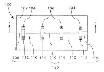
Fig. 1 is a top view of a stepped impedance filter formed on a
substrate for reducing the size of the stepped impedance filter in accordance
with the present invention.
Fig. 2 is a cross-sectional view of the stepped impedance filter of
Fig. 1 taken along line 2-2.
Fig. 3 is a cross-sectional view of an alternate embodiment of the
stepped impedance filter of Fig. 1 taken along line 2-2.
Fig. 4 is a cross-sectional view of an yet another embodiment of
the stepped impedance filter of Fig. 1 taken along line 2-2.
Fig. 5 is a flow chart that is useful for illustrating a process for
manufacturing a stepped impedance filter of reduced physical size in
accordance
with the present invention.
Fig. 6A is a graph including an insertion loss curve and a return
loss curve for a typical low pass stepped impedance filter.
Fig. 613 is a graph including an insertion loss curve and a return
loss curve achieved using substrate regions having different substrate
properties
in accordance with the present invention.
DETAILED DESCRIPTION OF THE PREFERRED EMBODIMENTS
A stepped impedance filter is commonly used in radio frequency
(RF) circuits and usually implemented on printed circuit boards or substrates.
Stepped impedance filters typically have an input port, an output port, and
multiple alternating high impedance and low impedance transmission line
sections. The length and width of each transmission line section, as well as
the
substrate characteristics of the circuit board where the transmission line
section
is coupled, can be adjusted to attain a desired impedance.
Low permittivity printed circuit board materials are ordinarily
selected for RF circuit designs implementing stepped impedance filters. For
example, polytetrafluoroethylene (PTFE) based composites such as RT/duroid
6002 (permittivity of 2.94; loss tangent of .009) and RT/duroid ~ 5880
(permittivity of 2.2; loss tangent of .0007) are both available from Rogers
-4-
CA 02432179 2003-06-12
Microwave Products, Advanced Circuit Materials Division, 100 S. Roosevelt
Ave, Chandler, AZ 85226. Both of these materials are common board material
choices. The above board materials provide substrate layers having relatively
low permittivities with accompanying low loss tangents.
However, use of conventional board materials can compromise the
miniaturization of circuit elements and may also compromise some performance
aspects of circuits that can benefit from high permittivity layers. A typical
tradeoff in a communications circuit is between the physical size of a stepped
impedance filter versus operational frequency. By comparison, the present
invention provides the circuit designer with an added level of flexibility by
permitting use of a high permittivity substrate layer region with magnetic
properties optimized for reducing the size of a stepped impedance filter for
operation at a specific frequency. Further, the present invention also
provides
the circuit designer with means for controlling the quality factar (Q) of the
stepped impedance filter. This added flexibility enables improved performance
and stepped impedance filter density and performance not othE:rwise possible
for
RF circuits. As defined herein, RF means any frequency that can be used to
propagate an electromagnetic wave.
Fig. 1 shows an exemplary stepped impedance filter 120 mounted
to substrate layer 100. The embodiment illustrated in Fig. 1 is a seven-
element
low-pass filter design for explanation purposes, however, it should be noted
that
the present invention is not limited with regard to the number of elements or
specific filter characteristics. The present invention can be used for any
type of
stepped impedance filter having any number of elements, for example high pass
filters, band pass filters, band notch filters, saw-tooth filters, comb
filters, etc.
The substrate layer 100 comprises a first region 102 having a first
set of substrate properties. One or more additional regions are included in
the
substrate layer to provide specific substrate properties proximate to
transmission
line sections. For example, second regions 104, each having a second set of
substrate properties, can be provided. Third regions 106 having a third set of
substrate properties also can be provided. Additional regions, each having
-5-
CA 02432179 2003-06-12
associated substrate properties, can be provided as well.
The substrate properties can include a generalized, complex valued
permittivity and permeability other than 1 +0j. Notably, the first, second and
third sets of substrate properties all can differ from each other. For
example, the
second regions 104 can have a higher permittivity and/or permeability than the
first region 102. The third regions 106 can have an even higher permittivity
and/or permeability.
The exemplary stepped impedance filter 120 comprises multiple
transmission line sections 1 10, 1 12 and 1 14 and input/output ports 108.
High
impedance transmission line sections 1 10 are coupled to the first region 102
and
lower impedance transmission line sections 1 12 are coupled tca the second
regions 104. Finally, lowest impedance transmission line sections 1 14 are
coupled to third regions 106, as shown. In this manner the substrate
properties
proximate to each transmission line section can be optimized for the impedance
requirements of each section.
Fig. 2 is a sectional view, shown along section line 2-2, of the
stepped impedance filter 120 and substrate layer 100 of Fig. 1 . A ground
plane
1 16 can be provided beneath the stepped impedance filter. Accordingly,
substrate layer 100 has a thickness that defines a stepped impedance filter
120
height above ground. The thickness is approximately equal to t:he physical
distance from the stepped impedance filter 120 to the underlying ground plane
1 16. This distance can be adjusted to achieve particular dielecaric
geometries,
for example, to increase or decrease capacitance when a certain dielectric
material is used.
An increase in permittivity in a particular region also increases the
capacitance of transmission line sections proximate to the region. Further, an
increase in the permeability of a particular region increases the inductance
of
transmission line sections proximate to the region as well. In another
embodiment (not shown), the stepped impedance filter can have its own
individual ground plane 1 16 or return trace (such as in a twin line
arrangement)
configured so that current on the ground plane 1 16 or return trace flows in
an
-6-
CA 02432179 2003-06-12
opposite direction to current flowing in the transmission line sections 1 10-1
14.
The opposite current flow will result in cancellation of magnetilc flux
associated
with the transmission line sections 1 10-1 14 and lower the inductance of
those
sections.
Accordingly, permittivity and permeability in each region can be
adjusted to attain desired capacitance and inductance values selected to
achieve
specific impedance characteristics for the correlating transmission line
segments.
For example, the capacitance and inductance can be adjusted to achieve a
desired Q for the stepped impedance filter response, which can be selected to
improve filter response.
In general, the propagation velocity of a signal traveling in a
transmission line Approximateiy inversely proportional to ,us . Since
propagation velocity is inversely proportion to relative permeability and
relative
permittivity, increasing the permeability and/or permittivity in the seiected
regions of the substrate layer 100 decreases propagation velocity of the
signal
on a transmission line segments coupled to the selected regions, and thus the
signal wavelength. Hence, the length and width of the transmission line
sections 1 10-1 14 can be reduced in size by increasing the permeability
and/or
permittivity of selected regions, for example second regions 1 C>4 and third
regions 106. Accordingly, the stepped impedance filter 120 c<~n be smaller,
both in length and width, than would otherwise be required on a conventional
circuit board.
The permittivity and/or permeability of the substrate layer 100 can
be differentially modified at selected regions to optimize stepped impedance
filter
performance. In yet another arrangement, all substrate layer regions can be
modified by differentially modifying permittivity and/or permeak>ility in all
regions
of the substrate layer.
The term "differential modifying" as used herein refers to any
modifications, including additions, to the substrate iayer 100 that result in
at
least one of the dielectric and magnetic properties being different at one
region
of the substrate as compared to another region. For example, 'the modification
CA 02432179 2003-06-12
can be a selective modification where certain substrate layer regions are
modified to produce a specific dielectric or magnetic properties, while other
substrate layer regions are left un-modified.
According to one embodiment, a supplemental dielectric layer can
be added to substrate layer 100. Techniques known in the art: such as various
spray technologies, spin-on technologies, various deposition technologies or
sputtering can be used to apply the supplemental layer. Referring to Fig. 3, a
first supplemental layer 302 can be added over the entire existing substrate
layer
100 and/or a second supplemental layer 304 can be selectively added in the
second and third regions 104 and 106, or selected portions thereof. The
supplemental layers 302 and 304 can be applied to result in a change of
permittivity and/or permeability for the dielectric beneath stepped impedance
filter 120. In an alternate embodiment, the supplemental layer can be added to
the first region 102 or selected portions thereof. For example, the
supplemental
layer can be added below the high impedance transmission line section and/or
input/output ports 108 to increase the permittivity and/or permeability in
those
regions.
Notably, the second supplemental layer 304 can include particles
306 to change the relative permeability in the first, second and/or third
regions
102-106 to be than1. For example, diamagnetic or ferromagnetic particles can
be added to any of the regions 102-106. Further, dielectric particles can be
added to any of the regions 102-106 as well. Additionally, the first
supplemental layer 302 and the second supplemental layer 304 can be provided
in any circuit configuration, for example stripline, microstrip and buried
microstrip.
An alternate embodiment of the present invention is shown in Fig.
4. Fourth substrate regions 402 can be provided proximate to the high
impedance transmission (ine sections 1 10. As with the other regions of the
substrate layer 100, the permttivity and permeability in the fourth substrate
regions 402 can be adjusted to achieve particular electrical characteristics
for
the high impedance transmission line sections 1 10. For example, the
_g_
CA 02432179 2003-06-12
permittivity and permeability of the fourth substrate regions can be adjusted
to
achieve a desired inductance, capacitance, impedance and/or « for the high
impedance transmission line sections 1 10.
A method for providing a size and performance optimized stepped
impedance filter is described with reference to the text below and the flow
chart
presented in Fig. 5. In step 510, board dielectric material is prepared for
modification. As previously noted, the board materiaB can include commercially
available off the shelf board material or customized board material formed
from a
polymer material, or some combination thereof. The preparation process can be
made dependent upon the type of board material selected.
In step 520, one or more substrate layer regions, such as the first,
second and third regions 102-106, can be differentially modified so that the
permittivity and/or permeability differ between two or more portions of the
regions. The differential modification can be accomplished in several
different
ways, as previously described. Referring to step 530, the metal layer then can
be applied to form the stepped impedance filter 120 using standard circuit
board
techniques known in the art.
Referring to Fig. 6A, an insertion loss curve 610 and a return loss
curve 615 curve is provided for a typical low pass stepped impedance fitter.
Fig.
6B shows an insertion loss curve 620 and a return loss curve 625 achieved
using substrate regions having different properties in accordance with the
present invention. As can be seen by comparing the graphs, a significant
improvement in filter performance is achieved using a substrate having regions
with differing substrate properties.
Dielectric substrate boards having meta-material regions providing
localized and selectable magnetic and substrate properties can be prepared in
the
following manner. As defined herein, the term "meta-materials°' refers
to
composite materials formed from the mixing or arrangement of two or more
different materials at a very fine level, such as the molecular or manometer
level.
Meta-materials allow tailoring of electromagnetic properties of the composite,
which can be defined by effective electromagnetic parameters comprising
_g_
CA 02432179 2003-06-12
effective electrical permittivity EEeff (or permittivity) and the effective
magnetic
permeability ~etf.
Appropriate bulk dielectric ceramic substrate materials can be
obtained from commercial materials manufacturers, such as DuPont and Ferro.
The unprocessed material, commonly called Green Taper"", can be cut into sized
regions from a bulk dielectric tape, such as into 6 inch by 6 inch regions.
For
example, DuPont Microcircuit Materials provides Green Tape rr~aterial systems,
such as 951 Low-Temperature Cofire Dielectric Tape and Ferro Electronic
Materials ULF28-30 Ultra Low Fire COG dielectric formulation. These substrate
materials can be used to provide substrate layers having relatively moderate
permittivities with accompanying relatively low loss tangents for circuit
operation
at microwave frequencies once fired.
In the process of creating a microwave circuit using multiple
sheets of dielectric substrate material, features such as vies, voids, holes,
or
cavities can be punched through one or more layers of tape. Voids can be
defined using mechanical means (e.g. punch) or directed energy means (e.g.,
laser drilling, photolithography), but voids can also be defined using any
other
suitable method. Some vies can reach through the entire thickness of the sized
substrate, while some voids can reach only through varying regions of the
substrate thickness.
The vies can then be filled with metal or other dielectric or
magnetic materials, or mixtures thereof, usually using stencils for precise
placement of the backfill materials. The individual layers of ta~>e can be
stacked
together in a conventional process to produce a complete, multi-layer
substrate.
Alternatively, individual layers of tape can be stacked together to produce an
incomplete, multi-layer substrate generally referred to as a sub-stack.
Voided regions can also remain voids. If backfilled with selected
materials, the selected materials preferably include mete-materials. The
choice
of a mete-material composition can provide controllable effective dielectric
constants over a relatively continuous range from less than 2 to at least
2650.
Controllable magnetic properties are also available from certain mete-
materials.
-10-
CA 02432179 2003-06-12
For example, through choice of suitable materials the relative effective
magnetic
permeability generally can range from about 4 to 1 16 for most practical RF
applications. However, the relative effective magnetic permeability can be as
low
as about 2 or reach into the thousands.
The term "differentially modified" as used herein refers to
modifications, including dopants, to a dielectric substrate layer that result
in at
least one of the dielectric and magnetic properties being different at one
region
of the substrate as compared to another region. A differentially modified
board
substrate preferably includes one or more meta-material containing regions.
For example, the modification can be selective rr~odification where
certain substrate layer regions are modified to produce a first s,et of
dielectric or
magnetic properties, while other substrate layer regions are modified
differentially or left unmodified to provide dielectric and/or magnetic
properties
different from the first set of properties. Differential modificatiion can be
accomplished in a variety of different ways.
According to one embodiment, a supplemental dielectric layer can
be added to the substrate layer. Techniques known in the art such as various
spray technologies, spin-on technologies, various deposition technologies or
sputtering can be used to apply the supplemental dielectric layer. The
supplemental dielectric layer can be selectively added in localized regions,
including inside voids or holes, or over the entire existing substrate layer.
For
example, a supplemental dielectric layer can be used for providing a substrate
region having an increased effective dielectric constant. The dielectric
material
added as a supplemental layer can include various polymeric materials.
The differential modifying step can further include locally adding
additional material to the substrate layer or supplemental dielecaric layer.
The
addition of material can be used to further control the effective dielectric
constant or magnetic properties of the substrate layer to achieve a given
design
objective.
The additional material can include a plurality of metallic and/or
ceramic particles. Metal particles preferably include iron, tungsten, cobalt,
-11-
CA 02432179 2003-06-12
vanadium, manganese, certain rare-earth metals, nickel or niobium particles.
The particles are preferably nanosize particles, generally having sub-micron
physical dimensions, hereafter referred to as nanoparticles.
The particles, such as nanoparticles, can preferably be
organofunctionalized composite particles. For example, organofunctionalized
composite particles can include particles having metallic cores with
electrically
insulating coatings or electrically insulating cores with a metallic coating.
Magnetic mete-material particles that are generally suitable for
controlling magnetic properties of substrate layer for a variety of
applications
described herein include ferrite organoceramics (FexCyHz)-(Ca/Sr/Ba-Ceramic).
These particles work well for applications in the frequency range of 8-40 GHz.
Alternatively, or in addition thereto, niobium organoceramics (~JbCyHz)-
(Ca/Sr/Ba-Ceramic) are useful for the frequency range of 12-40 GHz. The
materials designated for high frequency are also applicable to I~ow frequency
applications. These and other types of composite particles carp be obtained
commercially.
In general, coated particles are preferable for use: with the present
invention as they can aid in binding with a polymer matrix or side chain
moiety.
In addition to controlling the magnetic properties of the dielectric, the
added
particles can also be used to control the effective dielectric constant of the
material. Using a fill ratio of composite particles from approximately 1 to
70%,
it is possible to raise and possibly lower the dielectric constant of
substrate
substrate layer and/or supplemental dielectric layer regions significantly.
For
example, adding organofunctionaiized nanoparticles to a substrate layer can be
used to raise the dielectric constant of the modified substrate layer regions.
Particles can be applied by a variety of techniques including
polybiending, mixing and filling with agitation. For example, a dielectric
constant
may be raised from a value of 2 to as high as 10 by using a variety of
particles
with a fill ratio of up to about 70%. Metal oxides useful for thus purpose can
include aluminum oxide, calcium oxide, magnesium oxide, nickel oxide,
zirconium oxide and niobium (II, IV and V) oxide. Lithium niobate (LiNb03),
and
-12-
CA 02432179 2003-06-12
zirconates, such as calcium zirconate and magnesium zirconate, also may be
used.
The selectable substrate properties can be localized to areas as
small as about 10 nanometers, or cover large area regions, including the
entire
board substrate surface. Conventional techniques such as lithography and
etching along with deposition processing can be used for localized dielectric
and
magnetic property manipulation.
Materials can be prepared mixed with other materials or including
varying densities of voided regions (which generally introduce air) to produce
effective dielectric constants in a substantially continuous range from 2 to
about
2650, as well as other potentially desired substrate properties. For example,
materials exhibiting a low dielectric constant ( < 2 to about 4) include
silica with
varying densities of voided regions. Alumina with varying den;yities of voided
regions can provide a dielectric constant of about 4 to 9. Neither silica nor
1 5 alumina have any significant magnetic permeability. However, magnetic
particles can be added, such as up to 20 wt. %, to render these or any other
material significantly magnetic. For example, magnetic properties may be
tailored with organofunctionality. The impact on dielectric constant from
adding
magnetic materials generally results in an increase in the dielectric
constant.
Medium dielectric constant materials have a diePectric constant
generally in the range of 70 to 500 +/- 10%. As noted above these materials
may be mixed with other materials or voids to provide desired effective
dielectric
constant values. These materials can include ferrite doped calcium titanate.
Doping metals can include magnesium, strontium and niobium. These materials
have a range of 45 to 600 in relative magnetic permeability.
For high dielectric constant applications, ferrite or niobium doped
calcium or barium titanate zirconates can be used. These materials have a
dielectric constant of about 2200 to 2650. Doping percentages for these
materials are generally from about 1 to 10 %. As noted with respect to other
materials, these materials may be mixed with other materials or voids to
provide
desired effective dielectric constant values.
-13-
CA 02432179 2003-06-12
These materials can generally be modified through various
molecular modification processing. Modification processing can include void
creation followed by filling with materials such as carbon and i~luorine based
organo functional materials, such as polytetrafluoroethylene PTFE.
Alternatively or in addition to organofunctional integration,
processing can include solid freeform fabrication (SFF), photo, UV, x-ray, e-
beam
or ion-beam irradiation. Lithography can also be performed using photo, UV, x-
ray, e-beam or ion-beam radiation.
Different materials, including meta-materials, carp be applied to
different areas on substrate layers (sub-stacks), so that a plurality of areas
of the
substrate layers (sub-stacks) have different dielectric and/or magnetic
properties.
The backfill materials, such as noted above, may be used in conjunction with
-14-
CA 02432179 2003-06-12
one or more additional processing steps to attain desired, dielectric and/or
magnetic properties, either locally or over a bulk substrate region.
A top layer conductor print is then generally appllied to the
modified substrate layer, sub-stack, or complete stack. Conductor traces can
be
provided using thin film techniques, thick film techniques, electroplating or
any
other suitable technique. The processes used to define the conductor pattern
include, but are not limited to standard lithography and stencii.
A base plate is then generally obtained for collating and aligning a
plurality of modified board substrates. Alignment holes through each of the
plurality of substrate boards can be used for this purpose.
The plurality of layers of substrate, one or more sub-stacks, or
combination of layers and sub-stacks can then be laminated (e.g. mechanically
pressed) together using either isostatic pressure, which puts pressure on the
material from all directions, or uniaxial pressure, which puts prEasure on the
material from only one direction. The laminate substrate is then is further
processed as described above or placed into an oven to be fired to a
temperature
suitable for the processed substrate (approximately 850 C to 900 C for the
materials cited above).
The plurality of ceramic tape layers and stacked aub-stacks of
substrates can then be fired, using a suitable furnace that can Ibe controlled
to
rise in temperature at a rate suitable for the substrate materials used. The
process conditions used, such as the rate of increase in temperature, final
temperature, cool down profile, and any necessary holds, are selected mindful
of
the substrate material and any material backfilled therein or deposited
thereon.
Following firing, stacked substrate boards, typically, are inspected for flaws
using an optical microscope.
The stacked ceramic substrates can then be optionally diced into
cingulated pieces as small as required to meet circuit functional
requirements.
Following final inspection, the cingulated substrate pieces can i:hen be
mounted
to a test fixture for evaluation of their various characteristics, such as to
assure
that the dielectric, magnetic and/or electrical characteristics area within
specified
-15-
CA 02432179 2003-06-12
limits.
Thus, dielectric substrate materials can be provided with localized
selected dielectric and/or magnetic characteristics for improving the density
and
performance of circuits, including those comprising stepped impedance filters.
The dielectric flexibility allows independent optimization of circuit
elements.
While the preferred embodiments of the invention have been
illustrated and described, it will be clear that the invention is not so
limited.
Numerous modifications, changes, variations, substitutions and equivalents
will
occur to those skilled in the art without departing from the spirit and scope
of
the present invention as described in the claims.
-16-