Note: Descriptions are shown in the official language in which they were submitted.
CA 02432264 2003-06-12
HIGH EFFICIENCY RESONANT LINE
BACKGROUND OF THE IN1/ENTION
Statement of the Technical Field
The inventive arrangements relate generally to methods and
apparatus for providing increased design flexibility for RF circuits, and more
particularly for optimization of dielectric circuit board materials for
improved
performance in resonant lines.
Description of the Related Art
RF circuits, transmission lines and antenna elements are commonly
manufactured on specially designed substrate boards. For the purposes of these
types of circuits, it is important to maintain careful control over impedance
characteristics. If the impedance of different parts of the circuit do not
match,
this can result in inefficient power transfer, unnecessary heating of
components,
and other problems. Electrical length of transmission lines and radiators in
these
circuits can also be a critical design factor.
Two critical factors affecting the performance of a substrate
1 5 material are permittivity (sometimes called the relative permittivity or
s,. ) and the
loss tangent (sometimes referred to as the dissipation factor). The relative
permittivity determines 'the speed of the signal, arid therefore the
electrical
length of transmission lines and other components implemented on the
substrate. The loss tangent characterizes the amount of loss that occurs for
signals traversing the substrate material. Losses tend to increase with
increases
in frequency. Accordingly, low loss materials become even more important with
increasing frequency, particularly when designing receivE:r front ends and low
noise amplifier circuits.
Printed transmission 9ines, passive circuits and radiating elements
used in RF circuits are typically formed in one of tlhree ways. One
configuration
known as microstrip, places the signal line on a board surface and provides a
second conductive layer, commonly referred to as a ground plane. A second
_7_
CA 02432264 2003-06-12
type of configuration known as buried microstrip is similar except that the
signal
line is covered with a dielectric substrate material. In a third configuration
known as stripline, the signal line is sandwiched between two electrically
conductive (ground) planes. Ignoring loss, the characteristic impedance of a
transmission line, such as stripline or microstrip, is equal to Ll ~C~ where
Ll is
the inductance per unit length and C, is the capacitance per unit length. The
values of Ll and Cl are generally determined by the physical geometry and
spacing of the line structure as well as the permittivity cf the dielectric
materials) used to separate the transmission line structures. Conventional
substrate materials typically have a relative permeability of 1 Ø
In conventional RF design, a substrate material is selected that has
a relative permittivity value suitable for the design. Once the substrate
material
is selected, the line characteristic impedance value is exclusively adjusted
by
controlling the line geometry and physical structure.
1 5 Radio frequency (RF) circuits are typically embodied in hybrid
circuits in which a plurality of active and passive <circuit components are
mounted and connected together on a surface of .an electrically insulating
board
substrate such as a ceramic substrate. The various components are generally
interconnected by printed metallic conductors of copper, gold, or tantalum,
for
example that are transmission lines as stripline or microstrip or twin-line
structures.
The permittivity of the chosen subsi:rate material for a
transmission line, passive RF device, or radiating element determines the
physical wavelength of RF energy at a given frequency for that line structure.
One problem encountered when designing microelectronic RF circuitry is the
selection of a dielectric board substrate material that is optimized for all
of the
various passive components, radiating elements arid transmission line circuits
to
be formed on the board. In particular, the geometry of certain circuit
elements
may be physically large or miniaturized due to the unique electrical or
impedance
characteristics required for such elements. For example, many circuit elements
or tuned circuits may need to be an electrical 1 /4 wave. Similarly, the line
-2-
CA 02432264 2003-06-12
widths required for exceptionally high or low characteristic impedance values
can, in many instances, be too narrow or too wide respectively for practical
implementation for a given substrate. Since the physical size of the
microstrip
or stripline is inversely related to the relative permittivity of the
dielectric
material, the dimensions of a transmission line can be affected greatly by the
choice of substrate board material.
Still, an optimal board substrate material design choice for some
components may be inconsistent with the optimal board substrate material for
other components, such as antenna elements. M~areover, some design
objectives for a circuit component may be inconsistent vvith one another. For
example, it may be desirable to reduce the size of an ani:enna element. This
could be accomplished key selecting a board material with a relatively high
dielectric. However, the use of a dielectric with a higher relative
permittivity will
generally have the undesired effect of reducing the radiation efficiency of
the
antenna. Accordingly, the constraints of a circuit board substrate having
selected relative substrate properties often results in design compromises
that
can negatively affect the electrical performance and/or physical
characteristics
of the overall circuit.
An inherent problem with the foregoing approach is that, at least
with respect to the substrate material, the only control variable for line
impedance is the relative permittivity, s,.. This limitation highlights an
important
problem with conventional substrate materials, i.e. they fail to take
advantage of
the other factor that determines characteristic impedance, namely Ll , the
inductance per unit length of the transmission line.
Yet another problem that is encountered in RF circuit design is the
optimization of circuit camponents for operation on different RF frequency
bands. Line impedances and lengths that are optimized for a first RF frequency
band may provide inferior performance when used for other bands, either due to
impedance variations and/or variations in electrical length. Such limitations
can
limit the effective operational frequency range for .a given RF system.
-3-
CA 02432264 2003-06-12
Conventional circuit board substrates are generally formed by
processes such as casting or spray coating which generally result in uniform
substrate physical properties, including the permittivity. Accordingly,
conventional dielectric substrate arrangements for' RF circuits have proven to
be
a limitation in designing circuits that are optimal in regards to both
electrical and
physical size characteristics.
SIlMM~4RY OF THE INVENTION
The present invention relates to a circuit for processing radio
frequency signals. The resonant circuit includes a~ substrate where the
circuit
can be placed. The substrate can be a mesa material and can incorporate at
least one layer of substrate material. A resonant line and at least one ground
can be coupled to the substrate. An end of the resonant line can be
electrically
shorted to the ground or electrically open with respect to ground.
1 5 The substrate layer can include a first region with a first set of
substrate properties and at least a second region with a second set of
substrate
properties. The substrate properties can include permittivity and
permeability.
The second set of substrate properties can be different than the first set of
substrate properties and at least a portion of the resonant line can be
coupled to
the second region. Further, the first and/or second set of substrate
properties
can be differentially modified to vary a permittivity and/or a permeability
over a
selected region. A third region can be provided wiith a tf gird set of
substrate
properties as well. in one embodiment the third set of substrate properties
are
different than the second set of substrate properties.
The permittivity and/or permeability of the second region can be
higher or lower than the permittivity and/or permeability of the first region.
Likewise, the permittivity and/or permeability of the third region can be
higher or
lower than the permittivity and/or permeability of the second region. The
increased permittivities and/or permeabilities can rE:duce a size of the
resonant
line.
-4-
CA 02432264 2003-06-12
BRIEF DESCRIPTION OF THE DRAWINGS
Fig. 1 is a top view of a resonant line formed on a substrate for
reducing the size of the resonant line in accordance with the present
invention.
Fig. 2 is a cross-sectional view of an open-circuit configuration of
the resonant line of Fig. 1 taken along line A-A.
Fig. 3 is a cross-sectional view of a short circuit configuration of
the resonant line of Fig. 1 taken along line A-A.
Fig. 4 is a top view of an alternate embodiment of a resonant line
formed on a substrate for reducing the size of the resonant line in accordance
with the present invention.
Fig. 5 is a cross-sectional view of an open-circuit configuration of
the resonant line of Fig. 4 taken along line B-B.
Fig. 6 is a cross-sectional view of another alternate embodiment of
resonant line in accordance with the present invention.
Fig. 7 is a cross-sectional view of another alternate embodiment of
resonant line in accordance with the present invention.
Fig. 8 is a cross-sectional view of yet another embodiment of a
resonant line formed on a substrate for reducing the size of the resonant line
in
accordance with the present invention.
Fig. 9 is a flow chart that is useful for illustrating a process for
manufacturing a resonant line of reduced physical size in accordance with the
present invention.
DETAILED DESCRIPTION OF THE PREFERRED EMBODIMENTS
A resonant line is a transmission lines typically used in radio
frequency (RF) circuits. A resonant line is sometimes said to be resonant at
an
applied frequency, meaning the line has impedance; characteristics similar to
a
resonant circuit at that frequency. Notably, resonant line characteristics are
a
function of voltage reflections, not circuit resonane~e. On printed circuit
boards
or substrates, resonant lines are typically implemented by creating a line
with at
least one port at the input and either open-circuited or short-circuited to
ground
-5-
CA 02432264 2003-06-12
at the termination. The input impedance to an open or shorted resonant line is
typically resistive when the length of the resonant: line is an even or odd
multiple
of a quarter-wavelength of the operational frequency. That is, the input to
the
resonant line is at a position of voltage maxima or minima. When the input to
the resonant line is at a position between the voltage maxima and minima
points, the input impedance can have reactive cornponer~ts. For example,
properly chosen line segments may be used as parallel-resonant, series-
resonant,
inductive, or capacitive circuits, which is a very useful feature.
Low permittivity printed circuit board materials are ordinarily
selected for RF circuit designs. For example, polytetrafluoroethylene (PTFE)
based composites such as RT/duroid ~ 6002 (permittivity of 2.94; loss tangent
of .009) and RT/duroid ° 5880 (permittivity of 2.2:; loss tangent of
.0007) are
both available from Rogers Microwave Products, Advanced Circuit Materials
Division, 100 S. Roosevelt Ave, Chandler, AZ 85'.26. Both of these materials
1 5 are common board material choices. The above board materials provide
substrate layers having relatively Bow permittivities with accompanying low
loss
tangents.
However, use of conventional board materials can compromise the
miniaturization of circuit elements and may also compromise some performance
aspects of circuits that can benefit from high permittivity layers. A typical
tradeoff in a communications circuit is between the physical size of a
resonant
line versus operational frequency. By comparison, the present invention
provides the circuit designer with an added level of flexibility by permitting
use
of a high permittivity substrate layer region with rnagnetic properties
optimized
for reducing the size of a resonant line for operation at a specific
frequency.
Further, the present invention also provides the circuit designer with means
for
controlling the quality factor (Q) of the resonant line. This added
flexibility
enables improved performance and resonant line density and performance not
otherwise possible for radio frequency circuits (RF). As defined herein, radio
frequency means any frequency that can be used 1:o propagate an
electromagnetic wave.
-g_
CA 02432264 2003-06-12
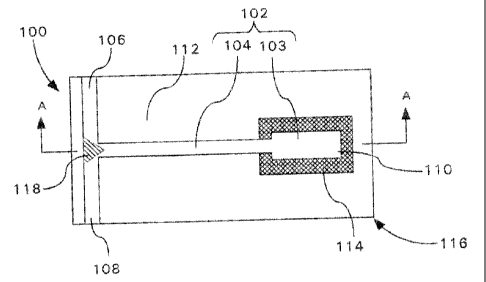
Referring to Fig. 1, according to the preferred embodiment a
substrate layer 100 comprises a first region 1 12 having a first set of
substrate
properties and a second region 1 14 having a second set of substrate
properties.
The substrate properties can include a permittivity and a permeability.
Notably,
the second set of substrate properties can be different than the first set of
substrate properties. For example, the second region 1 14 can have a higher or
lower permittivity and/or permeability that the first region 1 12.
Resonant line 102 is mounted on the substrate layer 100. In one
embodiment the resonant line 102 can be configured to have a stub 103 and a
trace 104. The stub 103 can be wider but shorter than the trace 104. Further,
the stub 103 can be configured to provide a capacitive termination for the
resonant line 102 or to achieve a particular impedance characteristic for the
resonant line 102. It will be appreciated by those skilled in the art,
however,
that the invention is not so limited and the resonant line also can be
configured
in differing shapes. For example, in one arrangement the resonant line can
have
a constant width trace vvithout a stub, can have a trace having an expanding
or
tapered width, or can have a geometrically shaped stub, for example circular.
Still, other resonant line shapes can be utilized.
The resonant line 102 also can connect to a first port 106 and a
second port 108. A transition zone 1 18 can be provided at the junction of the
ports 106, 108 and the resonant line 102 to improve the transition of signals
entering the resonant line 102 through the ports 106 and 108. The transition
zone can be a triangular cylinder as shown, or any other shape, for example a
round cylinder, oval cylinder or a sphere. The permittivity and/or
permeability of
the transition zone 1 18 cyan be controlled to reduce ringing and reflection
of
signals traveling through the ports 106 and 108. I=or example, the
permeability
of the transition zone 1 18 can be higher than the permeability of the first
region
112.
Resonant line 102 and the second region 1 14 of the substrate
layer 100 can be configured so that at least a portion of -the resonant line
102 is
positioned on the second region 1 14 as shown. In a preferred embodiment, at
_7_
CA 02432264 2003-06-12
least a substantial region of the resonant line 102 can be positioned on the
second region 1 14.
The propagation velocity of a signal traveling on the resonant line
is equal to ~ . Accordingly, increasing the permeability and/or
fc,.s,
permittivity in the second region 1 14 decreases propagation velocity of the
signal on the resonant line 102, and thus the signal wavelength. Hence, the
length of the resonant line 102 can be reduced by increasing the permeability
and/or permittivity. Thus the resonant line 102 can be smaller than would be
required on a conventional circuit board. The second region 1 14 also can have
a
permittivity selected to achieve particular capacitance characteristic. For
example, the permittivity in the second region 1 1 ~'_ can be increased to
reduce
the size of the stub 103 required to achieve a given capacitance value.
The permittivity andlor permeability can be chosen to result in a
desired Zo for the resonant line 102 as well, or to control capacitance,
inductance or resistance values associated with the resonant line 102. For
example, the cross sectional area of the resonant (line can be selected for a
particular resistance. Further, the substrate properties can be selected to
achieve a desired Q for particular resonances, shape the resonant response of
the resonant line 102, and/or adjust voltage maxima and minima. Further, the
substrate properties can be selected to suppress higher resonant modes and/or
to create a mismatch between the impedance of the resonant line 102 and the
impedance of free space. This impedance mismatch can help to minimize RF
radiation from the resonant line 102 and reduce electromagnetic interference
(EMI).
The resonant characteristics of the resonant line 102 can be
distributed through the first and second regions 1 12 and 1 14 as the electric
fields and magnetic fields formed in these regions atore and release energy.
The
amount of energy stored and released by the fields can be adjusted by
controlling permittivities and permeabilities associated with different
regions in
the substrate layer 100. For example, a higher per~mittivity in a particular
region
will result in greater energy stored in the electric fields formed in that
region.
_g_
CA 02432264 2003-06-12
Likewise, higher permeability in a particular region will result in greater
energy
stored in the magnetic fields formed in that region.
Figs. 2 and 3 are sectional views, shown along section line A-A,
of two different embodiments of the resonant fine 102 and substrate layer 100
of Fig. 1 . A ground plane 1 16 is provided beneath the resonant line 102 in
both
embodiments shown. The resonant line shown in Fig. 2 is an open-circuited
resonant line. The resonant line of Fig. 3 is a short-circuited with a
shorting
feed 300 provided to short the distal end 1 10 of the resonant line 102 to the
ground plane 116. A circuit designer can select either an open-circuited or
short-circuited resonant line, depending on the application, to provide the
voltage andlor impedance characteristics desired from the resonant line.
Substrate layer 100 has a thickness that defines a resonant line
height above ground. The thickness is approximately equal to the physical
distance from the resonant fine 102 to the underlying ground plane 1 16. This
1 5 distance can be adjusted to achieve particular dielectric geometries, for
example,
to increase or decrease capacitance when a certain dielectric material is
used.
Referring to Figs. 4 and 5, another arrangement for the resonant
line 102 is shown wherein the stub 103 is located within the second region 1
14
and positioned closer to the ground plane 1 16. This configuration can
increase
the capacitance between the stub 103 and the ground plane 1 16 while
maintaining a relatively low capacitance between trace 104 and the ground
plane 1 16. This configuration can be particularly useful for a capacitively
terminated resonant line. Alternatively, a buried m~icrostrip arrangement, as
shown in Fig. 6, can be used if higher capacitance between the trace 104 and
the ground plane 1 16 is desired. A stripline arrangement also can result in
an
increased capacitance value for both the trace 104 and the stub 103. A
shorting feed (not shown) can be provided in any of these configurations as
welt.
In one embodiment of the invention lthe permeability of the
substrate layer 100 can be controlled to increase tine inductance of all or
part of
the resonant line 102. In another embodiment (not shown), the resonant line
_g_
CA 02432264 2003-06-12
can have its own individual ground plane 1 16 or return trace (such as in a
twin
line arrangement) configured so that current on the ground plane 1 16 or
return
trace flows in an opposite direction to current flowing in the resonant line
102,
thereby resulting in cancellation of magnetic flux associated with the
resonant
line and lowering its inductance.
An alternate embodiment is shown iin Fig. 7 wherein a third region
710 is provided in the substrate layer 100. The embodiment shows a microstrip
configuration, but a third region 710 also can be provided in other
configurations, such as stripline and buried microstrip. In one arrangement
the
third region can have substrate properties differinci from the first region 1
12 and
the second region 1 14. For example, the permittivity and/or permeability in
the
third region 710 can be higher or lower than the permittivity and/or
permeability
in the first and second regions 1 1 Z and 1 14. In another arrangement, the
third
region 710 can have the same substrate properties as the second region 1 14.
1 5 For example, the third region 710 can comprise the same dielectric
material as
the second region 1 14 and thus have the same permittivity and/or
permeability.
The permittivities and/or permeabilities can be used to control the impedance
and resonant characteristics of the resonant line 102.
It should be noted that the resonant line 102 and circuit layer 100
configurations are not lirnited to the exemplary figures shown. For example,
the
resonant line can have varying shapes and can be positioned to have varying
distances between the resonant line and the ground plane or circuit layer
surface. in one embodiment, Zo can be controlled over the entire length of
resonant line 102, or any part thereof, using multiple dielectric and
ferromagnetic mixtures or concentrations to vary L:o over different regions of
the
line. Further, the permittivity and/or permeability c:an be differentially
modified
at selected regions of the substrate layer 100 to optimize resonant line
performance. In yet another arrangement, all substrate layer regions can be
modified by differentially modifying permittivity and/or permeability in all
regions
of the substrate layer 100.
The term '°differential modifying°' as used herein refers
to any
-10-
CA 02432264 2003-06-12
modifications, including additions, to the substrate layer 100 that result in
at
least one of the dielectric and magnetic properties being different at one
region
of the substrate as compared to another region. F=or example, the modification
can be selective modification where certain substrate layer regions are
modified
to produce a first set of dielectric or magnetic properties, while other
substrate
layer regions are left un-modified having dielectric and magnetic properties
different from the first set of properties resulting from the modification.
-11-
CA 02432264 2003-06-12
According to one embodiment, a supplemental dielectric layer can
be added to substrate layer 100. Techniques known in the art such as various
spray technologies, spin-on technologies, various deposition technologies or
sputtering can be used to apply the supplemental layer. Referring to Fig. 8, a
first supplemental layer 810 can be added over the entire existing substrate
layer
100 and/or a second supplemental layer 820 can Ibe selectively added in the
first
region 1 12, second region 1 14 and/or third region 710. The supplemental
layers
can change the perrnittivity and/or permeability of the dielectric beneath
line
102.
Notably, the second supplemental layer 820 can include particles
to change the permeability in the first, second ancllor third regions 1 12, 1
14 and
710. For example, diamagnetic or ferromagnetic particles can be added to any
of the regions 1 12, 1 14 and 710. Further, the second supplemental layer 820
can include dielectric particles to change the substrate properties as well.
For
example, dielectric particles can be added to any of the regions 1 12, 1 14
and
710. Further, the first supplemental layer 810 and the second supplemental
layer 820 can be provided in any circuit configurai~tion, for example
stripline,
microstrip and buried microstrip.
A method for providing a size and performance optimized resonant
line is described with reference to the text below and the flow chart
presented in
Fig. 9. In step 910, board dielectric material is prepared for modification.
As
previously noted, the board material can include commercially available off
the
shelf board material or customized board material formed from a polymer
material, or some combination thereof. The preparation process can be made
dependent upon the type of board material selected.
In step 920, one or more substrate Payer regions, such as the first,
second and/or third regions 1 12, 1 14 and 710, can be differentially modified
so
that the permittivity and/or permeability differ between two or more regions.
The differential modification can be accomplished in several different ways,
as
previously described. Referring to step 930, the metal layer then can be
applied
to the resonant line using standard circuit board techniques known in the art.
-12-
CA 02432264 2003-06-12
Substrate boards having metamaterial regions providing localized
and selectable magnetic and substrate properties can be prepared in the
following manner. As defined herein, the term "rr~etamaterials" refers to
composite materials formed from the mixing or arrangement of two or more
different materials at a very fine level, such as the molecular or nanometer
level.
Metamaterials allow tailoring of electromagnetic properties of the composite,
which can be defined by effective electromagnetic parameters comprising
effective electrical permittivity (or permittivity) and the effective magnetic
permeability.
Appropriate bulk dielectric substrate materials can be obtained
from commercial materials manufacturers, such as DuPont and Ferro. The
unprocessed material, commonly called Green TapeTM, can be cut into sized
regions from a bulk dielectric tape, such as into 6 inch by 6 inch regions.
For
example, DuPont Microcircuit Materials provides Green Tape material systems,
such as 951 Low-Temperature Cofire Dielectric Tape and Ferro Electronic
Materials ULF28-30 Ultra Low Fire COG dielectric formulation. These substrate
materials can be used to provide substrate layers having relatively moderate
permittivities with accompanying relatively low loss tangents for circuit
operation at microwave frepuencies ante fired.
In the process of creating a microwave circuit using multiple
sheets of dielectric substrate material, features such as vies, voids, holes,
or
cavities can be punched through one or more layers of tape. Voids can be
defined using mechanical means (e.g. punch) or directed energy means (e.g.,
laser drilling, photolithography), but voids can also be defined using any
other
suitable method. Some vies can reach through the entire thickness of the sized
substrate, while some voids can reach only through varying regions of the
substrate thickness.
The vies can then be filled with metal or other dielectric or
magnetic materials, or mixtures thereof, usually a sing stencils for precise
placement of the backfill materials. The individual layers of tape can be
stacked
together in a conventional process to produce a complete, multi-layer
substrate.
-13-
CA 02432264 2003-06-12
Alternatively, individual layers of tape can be stacked together to produce an
incomplete, multi-layer substrate generally referred to as a sub-stack.
Voided regions can also remain voids. If backfilled with selected
materials, the selected materials preferably include: metamaterials. The
choice of
a metamaterial composition can provide tunable effective dielectric constants
over a relatively continuous range from less than :? to about 2650. Materials
with magnetic properties are also available. For example, through choice of
suitable materials the relative effective magnetic permeability generally can
range from about 4 to 1 16 for most practical RF applications. However, the
relative effective magnetic permeability can be as low as about 2 or reach
into
the thousands.
The term '°differentialiy modified" as used herein refers to
modifications, including dopants, to a substrate layer that result in at least
one
of the dielectric and magnetic properties being different at one region of the
substrate as compared to another region. A differentially modified board
substrate preferably includes one or more metamaterial containing regions.
For example, the modification can be selective modification where
certain substrate layer regions are modified to produce a first set of
dielectric or
magnetic properties, while other substrate layer regions are modified
differentially or left unmodified to provide dielectric and/or magnetic
properties
different from the first set of properties. ~ifferential modification can be
accomplished in a variety of different ways.
According to one embodiment, a supplemental dielectric layer can
be added to the substrate layer. Techniques known in the art such as various
spray technologies, spin-on technologies, various deposition technologies or
sputtering can be used to apply the supplemental dielectric layer. The
supplemental dielectric Payer can be selectively added in localized regions,
including inside voids or holes, or over the entire existing substrate layer.
For
example, a supplemental dielectric layer can be used for providing a substrate
region having an increased effective dielectric constant. The dielectric
material
added as a supplemental layer can include various polymeric materials.
_~q._
CA 02432264 2003-06-12
The differential modifying step can f=urther include locally adding
additional material to the substrate layer or supplements! dielectric layer.
The
addition of material can be used to further control the effective dielectric
constant or magnetic properties of the substrate layer to achieve a given
design
objective.
The additional material can include a plurality of metallic and/or
ceramic particles. Metal particles preferably include iron, tungsten, cobalt,
vanadium, manganese, certain rare-earth metals, nickel or niobium particles.
The particles are preferably nanosize particles, generally having sub-micron
physical dimensions, hereafter referred to as nanoparticles.
The particles, such as nanoparticles, can preferably be
organofunctionalized composite particles. For example, organofunctionalized
composite particles can include particles having metallic cores with
electrically
insulating coatings or electrically insulating cores ~,rvith a metallic
coating.
1 5 Magnetic metamaterial particles that are generally suitable for
controlling magnetic properties of substrate layer 'for a variety of
applications
described herein include ferrite organoceramics (FexCyHz)-(Ca/Sr/Ba-CeramicD.
These particles work well for applications in the frequency range of 8-40 GHz.
Alternatively, or in addition thereto, niobium orgar~oceramics /NbCyliz)-
(Ca/Sr/Ba-Ceramic) are useful for the frequency range of 12-40 GNz. The
materials designated for high frequency are also applicable to low frequency
applications. These and other types of composite particles can be obtained
commercially.
In general, coated particles are preferable for use with the present
invention as they can aid in binding with a polymer matrix or side chain
moiety.
In addition to controlling the magnetic properties of the dielectric, the
added
particles can also be used to controi the effective dielectric constant of the
material. Using a fill ratio of composite particles from approximately 1 to
70%,
it is possible to raise and possibly lower the dielectric constant of
substrate layer
and/or supplemental dielectric layer regions significantly. For example,
adding
organofunctionalized nanoparticles to a substrate layer can be used to raise
the
-15_
CA 02432264 2003-06-12
dielectric constant of the modified substrate layer regions.
Particles can be applied by a variety of techniques including
polyblending, mixing and filling with agitation. For example, a dielectric
constant
may be raised from a value of 2 to as high as 10 by using a variety of
particles
with a fill ratio of up to about 70%. Metal oxides useful for this purpose can
include aluminum oxide, calcium oxide, magnesium oxide, nickel oxide,
zirconium oxide and niobium (Ii, IV and V) oxide. Lithium niobate (LiNbOs),
and
zirconates, such as calcium zirconate and magnesium zirconate, also may be
used.
The selectable substrate properties can be localized to areas as
small as about 10 nanometers, or cover large areas regions, including the
entire
board substrate surface. Conventional techniques such as lithography and
etching along with deposition processing can be used for localized dielectric
and
magnetic property manipulation.
Materials can be prepared mixed with other materials or including
varying densities of voided regions (which generally introduce air) to produce
effective dielectric constants in a substantially continuous range from 2 to
about
2650, as well as other potentially desired substrate properties. For example,
materials exhibiting a low dielectric constant ( < 2 to about 4) include
silica with
varying densities of voided regions. Alumina with varying densities of voided
regions can provide a dielectric constant of about 4 to 9. Neither silica nor
alumina have any significant magnetic permeability. However, magnetic
particles can be added, such as up to 20 wt. %, t~o render these or any other
material significantly magnetic. For example, magnetic properties may be
tailored with organofunctionality. The impact on dielectric constant from
adding
magnetic materials generally results in an increase in the dielectric
constant.
Medium dielectric constant materials have a dielectric constant
generally in the range of 70 to 500 +/- 10%. As noted above these materials
may be mixed with other materials or voids to provide desired effective
dielectric
constant values. These materials can include ferrite doped calcium titanate.
Doping metals can include magnesium, strontium and niobium. These materials
-16-
CA 02432264 2003-06-12
have a range of 45 to 600 in relative magnetic permeabirity.
CA 02432264 2003-06-12
For high dielectric constant applications, ferrite or niobium doped
calcium or barium titanate zirconates can be used.. These materials have a
dielectric constant of about 200 to 2650. Doping percentages for these
materials are generally from about 1 to 10 %. As noted with respect to other
materials, these materials may be mixed with other materials or voids to
provide
desired effective dielectric constant values.
These materials can generally be modified through various
molecular modification processing. Modification processing can include void
creation followed by filling with materials such as carbon and fluorine based
organo functional materials, such as pofytetrafluoroethylene PTFE.
Alternatively or in addition to organofunctional integration,
processing can include solid freeform fabrication (SFF), photo, uv, x-ray, e-
beam
or ion-beam irradiation. Lithography can also be performed using photo, uv, x-
ray, e-beam or ion-beam radiation.
Different materials, including rnetamaterials, can be applied to
different areas on substrate layers (sub-stacks), so that a plurality of areas
of the
substrate layers (sub-stacks) have different dielectric and/or magnetic
properties.
The backfill materials, such as noted above, may be used in conjunction with
one or more additional processing steps to attain desired, dielectric and/or
magnetic properties, either locally or over a bulk substrate region.
A top layer conductor print is then clenerally applied to the
modified substrate layer, sub-stack, or complete stack. Conductor traces can
be
provided using thin film techniques, thick film techniques, electroplating or
any
other suitable technique. The processes used to clefine the conductor pattern
include, but are not limited to standard lithography and stencil.
A base plate is then generally obtained for collating and aligning a
plurality of modified board substrates. Alignment holes through each of the
plurality of substrate boards can be used for this purpose.
The plurality of layers of substrate, one or more sub-stacks, or
combination of layers and sub-stacks can then be laminated (e.g. mechanically
pressed) together using either isostatic pressure, which puts pressure on the
-18-
CA 02432264 2003-06-12
material from all directions, or uniaxial pressure, ~nrhich puts pressure on
the
material from only one direction. The laminate substrate is then further
processed as described above or placed into an oven to be fired to a
temperature
suitable for the processed substrate lapproximately 850 C to 900 C for the
materials cited above).
The plurality of ceramic tape layers and stacked sub-stacks of
substrates can then be fired, using a suitable furnace that can be controlled
to
rise in temperature at a rate suitable for the substrate materials used. The
process conditions used, such as the rate of increase in temperature, final
temperature, cool down profile, and any necessary holds, are selected mindful
of
the substrate material and any material backfilled therein or deposited
thereon.
Following firing, stacked substrate boards, typically, are inspected for flaws
using an optical microscope.
The stacked ceramic substrates can then be optionally diced into
1 5 cingulated pieces as small as required to meet circuit functional
requirements.
Following final inspection, the cingulated substrate pieces can then be
mounted
to a test fixture for evaluation of their various characteristics, such as to
assure
that the dielectric, magnetic and/or electrical char;~cteristics are within
specified
limits.
Thus, dielectric substrate materials can be provided with localized
tunable dielectric and/or magnetic characteristics for improving the density
and
performance of circuits, including those comprising resonant lines. The
dielectric
flexibility allows independent optimization of the resonant lines.
While the preferred embodiments of the invention have been
illustrated and described, it will be clear that the invention is not so
limited.
Numerous modifications, changes, variations, substitutions and equivalents
will
occur to those skilled in the art without departing from the spirit and scope
of
the present invention as described in the claims.
_ 19-