Note: Descriptions are shown in the official language in which they were submitted.
CA 02432286 2003-06-18
WO 02/061805 PCT/US02/03161
HIGH POWER RADIATION EMITTER DEVICE AND HEAT
DISSIPATING PACKAGE FOR ELECTRONIC COMPONENTS
BACKGROUND OF THE INVENTION
[0001] The present invention generally relates to radiation emitter assemblies
such as,
for example, light emitting diode (LED) packages and to heat dissipating
packages for
electronic components.
[0002] Radiation emitters, particularly optical radiation emitters, are used
in a wide
variety of commercial and industrial products and systems and accordingly come
in
many forms and packages. As used herein, the term "optical radiation emitter"
includes
all emitter devices that emit visible light, near infrared (IR) radiation, and
ultraviolet
(UV) radiation. Such optical radiation emitters may be photoluminescent,
electroluminescent, or other solid state emitter. Photoluminescent sources
include
phosphorescent and fluorescent sources. Fluorescent sources include phosphors
and
fluorescent dyes, pigments, crystals, substrates, coatings, and other
materials.
[0003] Electroluminescent sources include semiconductor optical radiation
emitters and
other devices that emit optical radiation in response to electrical
excitation.
Semiconductor optical radiation emitters include light emitting diode (LED)
chips, light
emitting polymers (LEPs), organic light emitting devices (OLEDs), polymer
light
emitting devices (PLEDs), etc.
[0004] Semiconductor optical emitter components, particularly LED devices,
have
become commonplace in a wide variety of consumer and industrial opto-
electronic
applications. Other types of semiconductor optical emitter components,
including
OLEDs, LEPs, and the like, may also be packaged in discrete components
suitable as
substitutes for conventional inorganic LEDs in many of these applications.
[0005] Visible LED components of all colors are used alone or in small
clusters as status
indicators on such products as computer monitors, coffee makers, stereo
receivers, CD
players, VCRs, and the like. Such indicators are also found in a diversity of
systems
such as instrument panels in aircraft, trains, ships, cars, trucks, minivans
and sport
utility vehicles, etc. Addressable arrays containing hundreds or thousands of
visible
LED components are found in moving-message displays such as those found in
many
airports and stock market trading centers and also as high brightness large-
area outdoor
television screens found in many sports complexes and on some urban
billboards.
CA 02432286 2003-06-18
WO 02/061805 PCT/US02/03161
[0006] Amber, red, and red-orange emitting visible LEDs are used in arrays of
up to
100 components in visual signaling systems such as vehicle center high mounted
stop
lamps (CHMSLs), brake lamps, exterior turn signals and hazard flashers,
exterior
signaling mirrors, and for roadway construction hazard markers. Amber, red,
and blue-
green emitting visible LEDs are increasingly being used in much larger arrays
of up to
300 components as stop/slow/go lights at intersections in urban and suburban
intersections.
[0007] Multi-color combinations of pluralities of visible colored LEDs are
being used as
the source of projected white light for illumination in binary-complementary
and ternary
RGB illuminators. Such illuminators are useful as vehicle or aircraft
maplights, for
example, or as vehicle or aircraft reading or courtesy lights, cargo lights,
license plate
illuminators, backup lights, and exterior mirror puddle lights. Other
pertinent uses
include portable flashlights and other illuminator applications where rugged,
compact,
lightweight, high efficiency, long-life, low voltage sources of white
illumination are
needed. Phosphor-enhanced "white" LEDs may also be used in some of these
instances
as illuminators.
[0008] IR emitting LEDs are being used for remote control and communication in
such
devices as VCR, TV, CD, and other audio-visual remote control units.
Similarly, high
intensity IR-emitting LEDs are being used for communication between IRDA
devices
such as desktop, laptop and palmtop computers; PDAs (personal digital
assistants); and
computer peripherals such as printers, network adapters, pointing devices
("mice,"
trackballs, etc.), keyboards, and other computers. IR LED emitters and IR
receivers
also serve as sensors for proximity or presence in industrial control systems,
for location
or orientation within such opto-electronic devices such as pointing devices
and optical
encoders, and as read heads in such systems as barcode scanners. IR LED
emitters may
also be used in a night vision system for automobiles.
[0009] Blue, violet, and UV emitting LEDs and LED lasers are being used
extensively
for data storage and retrieval applications such as reading and writing to
high-density
optical storage disks.
[0010] Performance and reliability of LED components, chips, and systems are
heavily
influenced by the thermal performance of those components, chips, and systems,
and by
ambient temperature. Elevated operating temperatures simultaneously reduce the
emission efficiency of LEDs and increase the probability of failure in most
conditions.
-2-
CA 02432286 2003-06-18
WO 02/061805 PCT/US02/03161
This elevated temperature may be the result of high system thermal resistance
acting in
concert with internal LED power dissipation and may also be the result of high
ambient
operating temperature or other influence. Regardless of the cause, LED
efficiency and
reliability are normal adversely affected by increases in temperature. Thus,
it is
advantageous to minimize temperature rise of LED components, chips, and
systems
attributable to internal power dissipation during operation. This can be
accomplished by
reducing the conductive, convective, and radiative thermal resistance between
the LED
chip and ambient environment, such as by optimizing the materials and
construction of
the packaged device containing the LED chip. These methods, as applicable to
mass-
solderable, auto-insertable, and other discrete LED components, are disclosed
in
commonly assigned U.S. Patent No. 6,335,548, entitled "SEMICONDUCTOR
RADIATION EMITTER PACKAGE," filed on October 22, 1999, by John K. Roberts
et al., and published PCT International Publication No. WO 00/55914.
[0011] For high power LED systems and high power density LED systems, system
thermal performance is especially critical. LED illuminators and high power
signal
lights generating more than ten lumens (or more than one watt of power
dissipation) are
examples of systems which can benefit from improved thermal performance,
especially
if package area/volume must be minimized (increasing power density).
[0012] To limit the operational temperature of the LED, the power that is
allowed to be
dissipated through the LED is typically limited. To limit the dissipated
power, however,
the current that may be passed through the LED must be limited, which in turn
limits the
emitted flux of the LED since the emitted flux is typically proportional to
the electrical
current passed tlirough the LED.
[0013] Other fundamental properties of LEDs place further restrictions on the
useful
operational temperature change dT. Semiconductor LEDs, including IR, visible,
and UV
emitters, emit light via the physical mechanism of electro-luminescence. Their
emission
is characteristic of the band gap of the materials from which they are
composed and their
quantum efficiency varies inversely with their internal temperature. An
increase in LED
chip temperature results in a corresponding decrease in their emission
efficiency. This
effect is quite significant for all common types of LEDs for visible, UV, and
IR
emission. Commonly, a 1 C increase (dT) in chip temperature typically results
in up to
a 1 percent reduction in useful radiation and up to a 0.1 nm shift in the peak
wavelength
-3-
CA 02432286 2003-06-18
WO 02/061805 PCT/US02/03161
of the emission, assuming operation at a constant power. Thus, a dT of 40 C
can result
in up to a 40 percent reduction in emitted flux and a 4 nm shift in peak
wavelength.
[0014] From the preceding discussion, it can be seen that to avoid thermal
damage and
achieve optimal LED emission performance, it is very important to minimize the
AT
experienced by the LED device chip and package during operation. This may be
achieved by limiting power or reducing thermal resistance.
[0015] Limiting LED power, of course, is antithetical to the purpose of high
power
LEDs, i. e. , to produce more useful radiation. Generating higher flux with an
LED
generally requires higher current (and therefore higher power). Most prior art
devices,
however, exhibit relatively high thermal resistance from their semiconductor
radiation
emitter to ambient and are compelled to limit power dissipation in order to
avoid internal
damage. Thus, the best 5 mm T-13/4 THD packages are limited to about 110 mW
continuous power dissipation at 25 C ambient temperature.
[0016] An additional problem faced by designers of conventional LED devices is
that the
wire bond used to join one of the LED leads to the LED chip can break or lose
contact
with the lead or the chip. Such failure can occur, for example, due to shear
forces that
are transferred to the wire bond through the encapsulant or thermal
expansion/contraction of the encapsulant around the wire bond.
[0017] The other forms of radiation emitters mentioned above also experience
performance degradation, damage, increased failure probability or accelerated
decay if
exposed to excessive operating temperatures.
[0018] Consequently, it is desirable to provide a radiation emitter device
that has a
higher emission output than conventional LED devices while being less
susceptible to
failure due to a break in the wire bond contact or other defect that may be
caused by
excessive operating temperatures.
[0019] Similar heat dissipation problems exist with respect to other
electronic
components. For example, large heat sinks are often attached to
microprocessors of the
type used in personal computers. Accordingly, an improved heat dissipation
package for
such electronic components is desirable.
SUMMARY OF THE INVENTION
[0020] It is an aspect of the present invention to provide a relatively high
power and
high power density radiation emitter device capable of high radiant flux
and/or luminous
flux emission. It is a further aspect of the present invention to provide a
radiation
-4-
CA 02432286 2003-06-18
WO 02/061805 PCT/US02/03161
emitter device exhibiting relatively low temperature rise due to internal
power
dissipation and increased reliability by virtue of relatively low thermal
resistance. To
achieve these and other aspects and advantages in accordance with one
embodiment of
the present invention, the radiation emitting device of the present invention
comprises a
sealed chamber; one or more liquids or gels contained in the sealed chamber;
an
electroluminescent emitter that emits optical radiation in response to an
electrical signal,
the electroluminescent emitter is disposed in the sealed chamber in physical
and thermal
contact with one of the liquids or gels; and first and second electrical
conductors
electrically coupled to the electroluminescent emitter for energizing the
electroluminescent emitter. A portion of the structure defining the sealed
chamber may
be partially transparent to allow the radiation to enter or exit.
[0021] It is another aspect of the present invention to provide a package for
electronic
components having improved heat dissipation characteristics. To achieve these
and
other aspects and advantages, the electronic component package comprises first
and
second substrates sealed together and spaced apart to define a sealed chamber,
one or
more liquids or gels contained in the sealed chamber, and at least one
electronic
component disposed in the sealed chamber and thermal contact with one of the
liquids or
gels. According to one embodiment, the at least one electronic component
includes a
semi-conductor electronic component. According to another embodiment of the
invention, the first substrate is a printed circuit board.
[0022] According to another embodiment, an optical radiation emitting device
comprises: a sealed chamber; a fluid intermediary material contained in the
sealed
chamber and having a refractive index greater than 1.0; an electroluminescent
emitter
that emits optical radiation in response to an electrical signal, the
electroluminescent
emitter disposed in the sealed chamber in physical and thermal contact with
the fluid
intermediary material; and first and second electrical conductors electrically
coupled to
the electroluminescent emitter for energizing the electroluminescent emitter.
[0023] According to another embodiment, an optical radiation emitting device
comprises: a semiconductor radiation emitter that emits optical radiation in
response to
an electrical signal; a protective barrier for protecting the semiconductor
radiation
emitter, the protective barrier comprises a material that substantially
maintains its in-
band optical properties over time; and first and second electrical conductors
electrically
-5-
CA 02432286 2006-11-07
coupled to the semiconductor radiation eniitter for energizing the
semiconductor
radiation eniitter.
[0023.1) In one aspect of the present invention, there is provided an optical
radiation
emitting device comprising: a sealed chamber; a liquid or gel contained in
said sealed
chamber; an electroluminescent emitter that emits optical radiation in
response to an
electrical signal, said electroluminescent emitter disposed in said sealed
chamber in
physical and thermal contact with said liquid or gel; and first and second
electrical
conductors electrically coupled to said electroluminescent emitter for
energizing said
electroluminescent emitter.
[0023.21 In another aspect of the present invention, there is provided a
method of reducing
thermal resistance of a radiation emitter device, the method comprising the
steps of:
mounting the radiation emitter device on a substrate; and surrounding at least
a portion of
the radiation emitter device with a convective liquid or gel.
[0023.3J In yet another aspect of the present invention, there is provided a
vehicle headlamp
comprising: a sealed chamber; a liquid or gel contained in said sealed
chamber; a plurality
of optical radiation emitters that emits light in response to an electrical
signal, said light
sources disposed in said sealed chamber in physical and thermal contact with
said liquid
or gel; and first and second electrical conductors electrically coupled to
said optical
radiation emitters for energizing said optical radiation emitters.
[0024] These and other features, advantages, and objects of the present
invention will be
further understood and appreciated by those skilled in the art by reference to
the
following specification, claims, and appended drawings.
BRIEF DESCRIPTION OF THE DRAWINGS
[0025] In the drawings:
[00261 Fig. I is a top elevational view of a radiation emitting device
constructed in
accordance with a first embodiment of the present invention;
[0027] Fig. 2 is a perspective view of the radiation emitting device of first
embodiment
of the present invention;
[0028] Fig. 3A is a cross-sectional view taken along line HI-III" of the
radiation emitting
device shown in Fig. 1;
[0029] Fig. 3B is a cross-sectional view of an alternative embodiment of the
device
shown in Fig. 1;
-6-
CA 02432286 2006-11-07
[0030] Fig. 3C is a cross-sectional view of an alternative embodiment of the
device
shown in Fig. 1;
[0031] Fig. 4 is a cross-sectional view of a radiation emitter device
constructed in
accordance with a second enlbodiment of the present invention;
[0032] Fig. 5 is a cross-sectional view of a radiation emitter device
constructed in
accordance with a third embodiment of the present invention;
[0033] Fig. 6A is a cross-sectional view of a radiation emitter device
constructed in
accordance witli a first variation of a fourth embodiment of the present
invention;
[0034] Fig. 6B is a cross-sectional view of a radiation emitter device
constructed in
accordance with a second variation of a fourth embodiment of the present
invention;
[0035] Fig. 7 is a top view of a radiation emitter device constructed in
accordance with a
fifth embodiment of the present: invention;
[0036] Fig. 8 is a perspective view of a vehicle headlamp assembly constructed
in
accordance with the present invention;
[0037] Fig. 9 is a schematic diagram of an electrical circuit that may be
provided in one
or more of the above embodiments;
[0038] Fig. 10 is a top view of an initial package subassembly in accordance
with a sixth
embod'unent of the present invention;
-6a-
CA 02432286 2003-06-18
WO 02/061805 PCT/US02/03161
[0039] Fig. 11 is a top view of a finished package assembly constructed in
accordance
with the sixth embodiment of the present invention;
[0040] Fig. 12 is a graph illustrating the illuminance as a function of power
for the
package assembly shown in Fig. 11 with the chamber filled with liquid and with
the
sealed chamber not filled with any liquid;
[0041] Fig. 13 is a graph of the relative spectral irradiance as a function of
wavelength
obtained for the package assembly shown in Fig. 11 with the chamber not filled
with any
liquid for various power levels;
[0042] Fig. 14 is a graph of the relative spectral irradiance as a function of
wavelength
obtained for the package assembly shown in Fig. 11 with the chamber filled
with liquid
for various power levels;
[0043] Fig. 15 is a cross-sectional view of an alternative embodiment of the
device
shown in Fig. 1;
[0044] Fig. 16 is a plan view of a subassembly of the device shown in Fig. 15;
[0045] Fig. 17A is a cross-sectional view of an alternative embodiment of the
device
shown in Fig. 1;
[0046] Fig. 17B is a cross-sectional view of an alternative embodiment of the
device
shown in Fig. 1; and
[0047] Fig. 18 is a cross-sectional view of an electronic component package
assembly
constructed in accordance with an alternate embodiment of the present
invention.
DETAILED DESCRIPTION OF THE PREFERRED EMBODIMENTS
[0048] Reference will now be made in detail to the present preferred
embodiments of the
invention, examples of which are illustrated in the accompanying drawings.
Wherever'
possible, the same reference numerals will be used throughout the drawings to
refer to
the same or like parts.
[0049] For purposes of description herein, the terms "upper," "lower,"
"right," "left,"
"rear, " "front, " "vertical, " "horizontal, " "top, " "bottom, " and
derivatives thereof shall
relate to the invention as viewed by a person looking directly at the
radiation emitting
source along the principal optical axis of the source. However, it is to be
understood
that the invention may assume various alternative orientations, except where
expressly
specified to the contrary. It is also to be understood that the specific
device illustrated in
the attached drawings and described in the following specification is simply
an
exemplary embodiment of the inventive concepts defined in the appended claims.
-7-
CA 02432286 2003-06-18
WO 02/061805 PCT/US02/03161
Hence, specific dimensions, proportions, and other physical characteristics
relating to
the embodiment disclosed herein are not to be considered as limiting, unless
the claims
expressly state otherwise.
[0050] Several embodiments of the present invention generally relate to an
improved
optical radiation-emitting device useful in both high and low power
applications. Such
embodiments of the present invention are particularly well suited for use in
limited
power applications such as vehicles, portable lamps, and specialty lighting.
By vehicles,
we mean over-land vehicles, watercraft, aircraft and manned spacecraft,
including but
not limited to automobiles, trucks, vans, buses, recreational vehicles (RVs),
bicycles,
motorcycles and mopeds, motorized carts, electric cars, electric carts,
electric bicycles,
ships, boats, hovercraft, submarines, airplanes, helicopters, space stations,
shuttlecraft
and the like. By portable lamps, we mean camping lanterns, head or helmet-
mounted
lamps such as for mining, mountaineering, and spelunking, hand-held
flashlights and the
like. By specialty lighting we mean emergency lighting activated during power
failures,
fires or smoke accumulations in buildings, microscope stage illuminators,
billboard
front-lighting, backlighting for signs, etc. The light emitting assembly of
the present
invention may be used as either an illuminator or an indicator. Examples of
some of the
applications in which the present invention may be utilized, are disclosed in
commonly
assigned PCT International Publication No. WO 00/55685 entitled "INDICATORS
AND ILLUMINATORS USING A SEMICONDUCTOR RADIATION EMITTER
PACKAGE," by John K. Roberts et al.
0
[0051] Some of the embodiments of the present invention provide a highly
reliable, low-
voltage, long-lived, light source for vehicles, portable lighting, and
specialty lighting
capable of producing white light with sufficient luminous intensity to
illuminate subjects
of interest well enough to be seen and to have sufficient apparent color and
contrast so as
to be readily identifiable. Several of the radiation emitter devices of the
present
invention may be well suited for use with AC or DC power sources, pulse-width
modulated DC power sources, and electronic control systems. The radiation
emitting
devices of the present invention may further be used to emit light of various
colors
and/or to emit non-visible radiation such as IR and UV radiation.
[0052] As used herein, the term "radiation emitter" and "radiation emitting
device"
shall include any structure that generates and emits optical or non-optical
radiation,
while the term "optical radiation emitter" or "optical radiation emitting
device" includes
-8-
CA 02432286 2003-06-18
WO 02/061805 PCT/US02/03161
those radiation emitters that emit optical radiation, which includes visible
light, near
infrared (IR) radiation, and/or ultraviolet (UV) radiation. As noted above,
optical
radiation emitters may include electroluminescent sources or other solid-state
sources
and/or photoluminescent or other sources. One form of electroluminescent
source
includes semiconductor optical radiation emitters. For purposes of the present
invention,
"semiconductor optical radiation emitters" comprise any semiconductor
component or
material that emits electromagnetic radiation having a wavelength between 100
nm and
2000 nm by the physical mechanism of electroluminescence, upon passage of
electrical
current through the component or material. The principle function of a
semiconductor
optical radiation emitter within the present invention is the conversion of
conducted
electrical power to radiated optical power. A semiconductor optical radiation
emitter
may include a typical IR, visible or UV LED chip or die well known in the art
and used
in a wide variety of prior art devices, or it may include any alternate form
of
semiconductor optical radiation emitter as described below.
[0053] Alternate forms of semiconductor optical radiation emitters which may
be used in
the present invention are light emitting polymers (LEPs), polymer light
emitting diodes
(PLEDs), organic light emitting diodes (OLEDs) and the like. Such materials
and
optoelectronic structures made from them are electrically similar to
traditional inorganic
LEDs, but rely on organic compositions such as derivatives of the conductive
polymer
polyaniline for electroluminescence. Such semiconductor optical radiation
emitters are
relatively new, but may be obtained from sources such as Cambridge Display
Technology, Ltd. of Cambridge, and from Uniax of Santa Barbara, California.
[0054] For brevity, the term semiconductor optical radiation emitter may be
substituted
with the term LED or the alternate forms of emitters described above or known
in the
art. Examples of emitters suitable for the present invention include varieties
of LED
chips with associated conductive pads for electrical attachment and that are
emissive
principally at P-N or N-P junctions within doped inorganic compounds of
AlGaAs,
AlInGaP, GaAs, GaP, InGaN, AlInGaN, GaN, SiC, ZnSe and the like.
[0055] LEDs are a preferred electroluminescent light source for use in the
radiation
emitting devices of the present invention because LEDs do not suffer
appreciable
reliability or field-service life degradation when mechanically or
electronically switched
on and off for millions of cycles. The luminous intensity and illuminance from
LEDs
closely approximates a linear response function with respect to applied
electrical current
-9-
CA 02432286 2003-06-18
WO 02/061805 PCT/US02/03161
over a broad range of conditions, making control of their intensity a
relatively simple
matter. Finally, recent generations of AlInGaP, AIGaAs, InGaN, AlInGaN, and
GaN
LEDs draw less electrical power per lumen or candela of visible light produced
than
incandescent lamps, resulting in more cost-effective, compact, and lightweight
illuminator wiring harnesses, fuses, connectors, batteries, generators,
alternators,
switches, electronic controls, and optics. A number of examples have
previously been
mentioned and are incorporated within the scope of the present invention,
although it
should be recognized that the present invention has obvious other applications
beyond
the specific ones mentioned which do not deviate appreciably from the
teachings herein
and therefore are included in the scope of this invention.
[0056] Another preferred radiation source that may be used in the inventive
light
emitting assembly is a photoluminescent source. Photoluminescent sources
produce
visible light by partially absorbing visible or invisible radiation and re-
emitting visible
radiation. Photoluminescent sources phosphorescent and fluorescent materials,
which
include fluorescent dyes, pigments, crystals, substrates, coatings, as well as
phosphors.
Such a fluorescent or phosphorescent material may be excited by an LED or
other
radiation emitter and may be disposed within or on the LED, or within or on a
separate
optical element, such as a lens or diffuser that is not integral with an LED.
Exemplary
structures using a fluorescent or phosphorescent source are described further
below.
[0057] As explained in more detail below, the present invention exhibits a
significantly
lower thermal resistance than conventional LED structures by extracting heat
from the
LED chip(s) via all of the surfaces of the LED chip(s) simultaneously instead
of from
primarily only one surface as in typical prior art LED devices. More
specifically, the
radiation emitter package of the present invention provides a sealed chamber
or cavity
containing a liquid or gel surrounding the LED chips, the liquid or gel having
a
moderate to high thermal conductivity, a moderate to high convectivity, or
botli. A
material that is "moderate to highly convective" is a material that is more
effectively
convective than either air or a conventional clear solid polymer such as epoxy
or
silicone. "Effectively convective" means transporting substantial proportions
of heat
dissipated from a source by natural convection. The LED chips may be mounted
to a
moderate to high thermal conductivity plate to which a transparent plate is
sealed in
spaced-apart relation to define the sealed chamber or cavity. This combination
is
uniquely effective because heat is removed from large surfaces of the chip by
conduction
-10-
CA 02432286 2003-06-18
WO 02/061805 PCT/US02/03161
and by convective transport due to the natural convection of the liquid in the
sealed
chamber or cavity. Embodiments of the present invention are discussed below in
connection with Figs. 1-18. It will be appreciated that these embodiments are
provided
for purposes of illustration only and are not limiting to the present
invention.
[0058] Figs. 1-3 show a radiation emitter device 10 constructed in accordance
with a
first embodiment of the present invention. Device 10 includes one or more
radiation
emitting sources 12, which are shown in Fig. 1 mounted to a first substrate
14.
Although radiation emitters 12 are preferably LED chips or dies, other forms
of
radiation emitters may be used. The LED chips may be any conventional LED chip
including those with vertical and lateral structure, transparent or absorbing
substrate,
electrically conductive or insulating substrate, tapered sides, Truncated
Inverted Pyramid
(TIP) construction, partial TIP construction, or flip chip, or other chip
geometry,
including LED chips utilizing AlGaAs, AIInGaP, GaAs, GaP, InGaN, AlInGaN, GaN,
SiC, ZnSe and other inorganic compound semiconductor materials. The anode can
be
on the topmost surface of the chip, normally used for wirebond, and the
cathode may be
on the bottom of the chip, normally connected with die attach adhesive, solder
or
eutectic bonding. As with some InGaN/SiC LED chips, this polarity may be
reversed
such that the cathode is at the topside, normally used for wirebond and the
anode is at
the bottom, normally connected with die attach adhesive, solder or eutectic
bonding.
Alternately, both anode and cathode may be topside of the chip as in a lateral
type
InGaN/sapphire LED chip structure, normally connected by wirebonding. Both
contacts
may also be at the bottom side of the chip in flip-chip configuration, and
normally
attached with solder or die attach adhesive. LED chips suitable for use in the
present
invention included are available from sources such as Cree, AXTI, UOE,
LumiLEDS
and UEC and others. For purposes of this first embodiment, first substrate 14
may be
made of any electrically conductive material, and preferably a material that
has relatively
high thermal conductivity. Preferably, first substrate 14 has a thickness of
0.5 to 6.1
mm and is made of copper or aluminum. As described below with respect to other
embodiments, the first substrate may alternately be made of electrically
nonconductive
material (such as a ceramic, PC board, passivated metal clad board, etc.). The
first
substrate may also comprise all or a portion of or surface of an external
cooling structure
such as a heat sink or thermoelectric cooler. An optional submount made of
silicon,
silicon carbide, metal or other like materials, may be mounted between
emitters 12 and
-11-
CA 02432286 2003-06-18
WO 02/061805 PCT/US02/03161
first substrate 14 to facilitate distribution of electrical power or to
moderate the physical
properties of the emitters and the first substrate.
[0059] Radiation emitter assembly 10 further includes a second substrate 16
serving as a
protective barrier that is spaced apart from first substrate 14. At least a
portion of
second substrate 16 through which radiation is emitted from radiation emitters
12 is
substantially transparent to some or all of the wavelengths of radiation
emitted from
emitters 12. Alternatively, all of second substrate 16 may be transparent to
the radiation
emitted from radiation emitters 12 or alternatively transparent to all
visible, IR, and/or
UV radiation. For example, second substrate 16 may be made of a 0.5 to 6.1 mm
glass
cover plate. For some embodiments, this glass may be conventional soda-lime
float
glass, and in others it may be fused silica glass, borosilicate float glass or
other glass
composition. Second substrate may also be made of tempered glass, an epoxy
sheet, or
transparent plastics that are aliphatic or olefinic in nature (e.g.,
polypropylene,
polyethylene, dicylcopentadienes and polymethylpentenes). Such transparent
aliphatic or
olefinic plastics do not degrade when exposed to aprotic solvents such as
propylene
carbonate, which is one possible liquid that may be used in the present
invention. These
transparent plastics also function well in solid-state systems that include
pure solution-
phase and partial solution-phase electrolytes. These transparent plastics
include: cyclic
olefin copolymers such as TOPAS available from Ticona, LLC of Summitt, New
Jersey; polymethylpentenes such as TPX' manufactured by Mitsui; hydrogenated
cyclo-
olefin polymers such as ZEONEX (based on dicyclopentadiene) manufactured by
Nippon Zeon Company; and amorphous cycloolefin copolymers such as APELI
manufactured by Mitsui. Another suitable polymer for the second substrate is
polysulfone. Second substrate 16 should maintain its "in-band" optical
properties over
an extended period of time. The term "in-band" optical properties shall mean
those
optical properties that affect or substantially influence radiation at
wavelengths emitted
by the radiation emitters within the assembly. Specifically, it should
maintain an
absence of optical absorption (particularly, at the wavelength emitted by
radiation
sources within the assembly), be resistant to hazing and scattering, and be
resistant to
reactions that cause it to turn yellow or otller color over time in such a
manner as to
unintentionally absorb significant portions of radiation emitted by light
sources within
the assembly. In many embodiments, second substrate 16 should be resistant to
degradation upon prolonged, repeated or intense exposure to short-wavelength
radiation
-12-
CA 02432286 2003-06-18
WO 02/061805 PCT/US02/03161
such as blue, violet or UV light or upon exposure to ambient heat, heat from
processing
the assembly or from internal heat generated by operating the assembly. For
embodiments of the present invention containing emitters of blue-green, blue,
violet or
UV light, it may be especially important for the second substrate 16 to start
and remain
substantially transparent in the short. wavelength bands emitted, avoiding the
yellowing
phenomena typical of some transparent polymer materials, and thus avoiding
excessive
tendencies toward increased absorption of radiation produced by those
emitters. Second
substrate 16 may also be treated with a coating (not shown), such as an anti-
reflection
coating, a barrier coating or other thin-film coating, on one or more of its
surfaces.
Such a coating may be employed, for example to enhance extraction efficiency
for
optical radiation emitted by sources within the chamber 21 and exiting through
surfaces
of second substrate 16. Another coating may be used to prevent permeation of
oxygen,
water vapor or other agents through second substrate 16 into the chaxnber 21,
to prevent
impurities from leaching out of second substrate 16 into liquid 20, or to
prevent portions
of liquid 20 from permeating into or reacting with second substrate 16.
[0060] Second substrate 16 is generally semi-rigid to rigid, however it may be
advantageous in some embodiments for second substrate 16 to be made
substantially
flexible. By making second substrate 16 flexible, it may be possible to
accommodate
bulk thermal expansion of liquid 20 as may occur during prolonged operation of
the
assembly at high power levels, or during operation in environments having an
ambient
temperature greater than that prevailing during the manufacture of the
assembly. Such
flexibility may be accomplished by utilizing thinner sheets of transparent
material for
construction of second substrate 16 or by choosing more flexible materials to
begin with.
Alternately, second substrate 16 may be made flexible by increasing the area
of the
chamber 21 in such a way that portions of second substrate 16 are disposed at
considerable distance from retaining forces applied by seal 18 (or by otlier
mechanisms
in the vicinity of seal 18).
[0061] As shown in Figs. 1-3, assembly 10 further includes a seal (or gasket)
18
extending between first and second substrates 14 and 16 so as to define a
closed region
therebetween that is hereinafter referred to as a "sealed chamber." As used
herein, the
term "chamber" may include a cavity or similar structure. The seal or gasket
18 is
preferably made of epoxy, butyl rubber, a frit of metallic and/or glassy
composition,
ceramic, metal alloys such as solder, or other relatively inert barrier
material. Within
-13-
CA 02432286 2003-06-18
WO 02/061805 PCT/US02/03161
the sealed chamber is a liquid, gel, or other material that is either moderate
to highly
thermally conductive, moderate to highly convective, or both. As used herein,
a "gel" is
a medium having a solid structure and a liquid permeating the solid structure.
Because a
gel includes a liquid, the term liquid is used hereinafter to refer to liquids
contained in
gels as well as non-gelled liquids.
[0062] The liquid 20 is disposed within the sealed chamber 21 so as to
surround each of
the LED chips 12 used in the device. Enough liquid 20 may be disposed within
the
sealed chamber 21 such that the sealed chamber 21 is effectively filled.
Alternately, the
volume of liquid 20 used may be less than the volume of the sealed chamber 21
such that
a portion of the sealed chamber 21 remains occupied by a bubble of air, gas or
vacuum
(not shown). Such an unfilled portion of the chamber 21 may be useful for
accommodating thermal expansion of the liquid 20 or as a visual indication
that the
remainder of the chamber 21 is filled. More than one type of liquid 20 may
also be used
within the same sealed chamber 21 such that more than one zone is defined (not
shown),
and occupied by a such liquids if they are not miscible. Such a configuration
may be
useful if different physical, optical or chemical properties are desired for
the liquid 20
present in different portions of the chamber 21. Liquid 20 is preferably, but
not
necessarily, electrically nonconductive. The materials utilized for substrates
14 and 16,
seal 18, and LED chips 12 preferably are selected such that they do not react
or
otherwise ionize the liquid 20 so as to cause the liquid to become
significantly
electrically conductive. High electrical conductivity of liquid 20 could
create a short
circuit across the LED chips 12 depending upon how they are disposed in the
sealed
chamber 21. Preferably, liquid 20 has low to moderate thermal expansion, or a
thermal
expansion that substantially matches that of first substrate 14, second
substrates 16, or
seal 18, and in some embodiments, a slightly higher thermal expansion may be
desired
to increase convection while in other embodiments, a low coefficient of
thermal
expansion may be desired to minimize stress on the optional die attach (not
shown),
optional solder bumps (25) and seal 18. Liquid 20 is also preferably inert and
does not
readily decompose or otherwise react with external agents that manage to enter
the
sealed chamber 21 over time or with impurities contained within the sealed
chamber 21
from the time of manufacture. Liquid 20 should also maintain its optical
properties over
time. Specifically, it should be resistant to reactions that cause the liquid
to turn yellow
or other color over time in such a manner as to unintentionally absorb
significant
-14-
CA 02432286 2003-06-18
WO 02/061805 PCT/US02/03161
portions of radiation emitted by light sources within the assembly. For
applications
where the assembly will be exposed to short wavelength radiation such as UV,
violet,
blue or blue-green optical radiation from the ambient environment or from
emitters
within the assembly, liquid 20 should be resistant to degradation upon
prolonged,
repeated or intense exposure such radiation. For embodiments of the present
invention
containing emitters of blue-green, blue, violet or UV light, it may be
especially
important for the liquid 20 to remain substantially colorless, avoiding
excessive
tendencies toward increased absorption of radiation produced by those
emitters. Liquid
20 should also be compatible with the seal material. The liquid should also be
substantially transparent to some or all of the wavelengths of radiation
emitted from the
radiation emitters 12. It will be appreciated however, that liquids may be
selected or
dyes may be utilized to selectively filter the radiation emitted from the
radiation emitters
12. Liquid 20 also preferably has an index of refraction between that of the
radiation
emitters 12 and the glass or otherwise have an index that approximately
matches one of
the emitters or the glass. Another benefit that may result from providing
liquid 20 in
contact with emitters 12 and any optional wire bond, is that the liquid
provides viscous
damping of any vibration of the wire bond. Additionally, liquid 20 (also
referred to
herein as an intermediary material that is disposed between the emitter(s) and
the second
substrate or protective barrier) may provide increased optical extraction
efficiency by
minimizing internal reflection within the device. In this respect, it should
be noted that
most LED chip materials possess high refractive indices, such that greater
light
extraction losses occur by total internal reflection and internal absorption
when such
chips are surrounded by media with very low refractive indices. Air or other
atmospheric gasses typically have a refractive index near 1.0 such that a
configuration
involving juxtaposition of LED chips directly against air leads to poor
optical coupling.
For this reason, liquid 20 is selected to have a relatively higher refractive
index,
consistent with other functional requirements. The refractive index of liquid
20 at the
emission wavelength of sources within the assembly is generally higher than
about 1.3,
but is more preferably higher than 1.4 and in some cases may be higher than
1.5. With
addition of small-particle fillers or other additives, liquid 20 may become a
suspension
or solution with an effective refractive index as high as 2.5. Such additives
may include
inorganic fillers or organic materials, including nanoparticles, doped
nanocrystals,
conventional phosphors. Certain types of optical fluids such as oils may also
be
-15-
CA 02432286 2003-06-18
WO 02/061805 PCT/US02/03161
available with or without such fillers or additives and having elevated
refractive indices
greater than 1.4 and as high as 3Ø Liquid 20 may be propylene carbonate or
another
liquid or gel having one or more of the above described properties. One
commercially
available liquid that may be used is Galden D02TS available from Montedison
S.P.A.
of Milan, Italy.
[0063] The liquid 20 may be dispensed within the sealed chamber 21 by vacuum
back-
filling or other conventional techniques such as those used to dispense an
electrochromic
solution between two glass substrates when making an electrochromic mirror or
window.
One or more fill holes may be provided in either the seal or in one or both of
the
substrates. After the sealed chamber 21 is filled with liquid 20, the hole(s)
may be
plugged with a UV-curable or other plug material.
[0064] In the embodiment shown in Figs. 1-3, the substrates are approximately
one inch
by one and one quarter inch rectangles. The size of the substrates may,
however, be
much bigger and be as large as an architectural window or the like, or may be
smaller
depending on the application. Preferably, the volume of liquid in the sealed
chamber 21
defined by the seal and the two substrates is more than about 20 times greater
than the
volume of the radiation emitters to ensure sufficient heat transport. In some
embodiments, it may be possible to reduce this volume as low as 2 times the
volume of
the radiation emitters. Although substrates 14 and 16 are depicted in Figs. 1
and 2 as
being rectangular, it will be appreciated that the substrates may have
virtually any shape.
Square, circular, hexagonal and octagonal shapes may be desirable in specific
applications. Seal 18 need not be formed in the same shape as that of the
substrates.
Seal 18 serves to bond the two substrates together and form sides of the
sealed chamber
21 in which liquid 20 is contained. Seal 18 should also serve as an
environmental
barrier so as to impede diffusion of water, oxygen, and other substances into
the sealed
chamber 21 while also impeding liquid 20 from exiting the sealed chamber 21.
Seal 18
may also function as a spacer for maintaining the separation distance of
substrates 14 and
16. Spacers (not shown) in the form of pillars, glass beads, etc. disposed
between the
substrates may be used as the sole means for maintaining the separation
distance of
substrates 14 and 16 or as a supplement to the spacing function served by the
seal. The
radiation emitters or other electrical components in the sealed chamber 21
(described
further below) may also provide this spacing function.
-16-
CA 02432286 2003-06-18
WO 02/061805 PCT/US02/03161
[0065] To enable electrical current to flow to and through any
electroluminescent
radiation emitters 12 that may be present in the sealed chamber 21, electrical
conductors
are provided that are electrically coupled to emitters 12 and extend out from
the sealed
chamber 21. When an electrically conductive first substrate 14 is utilized,
the negative
or positive terminal of the emitters 12 may be directly mounted to first
substrate 14
while the other of the terminal of emitters 12 may be soldered (note solder
bumps 25) or
otherwise electrically connected to a conductor 22 provided on the bottom
inner surface
of second substrate 16. Conductor 22 may be made of metal or made of indium
tin
oxide (ITO), which is a common transparent conductor. With such a
configuration, the
spacing between first substrate 14 and second substrate 16 would be
approximately equal
to the thickness of emitters 12, which is typically on the order of 0.012
inch, but may be
as low as 0.001 inch or as high as 0.500 inch. In this embodiment, partial
conductivity
of liquid 20 may supplement or serve as the replacement for solder bumps 25 at
the top
of the emitters 12 making electrical connection to conductor(s) 22 on second
substrate
16.
[0066] As shown in Fig. 2, electrical leads 26 and 30 may be coupled to
electrical
conductor 22 and first substrate 14 by respective conductive clips 24 and 28.
Such clips
may have a construction similar to those utilized in electrochromic devices.
An example
of suitable clips is disclosed in U.S. Patent No. 6,064,509 entitled "CLIP FOR
USE
WITH TRANSPARENT CONDUCTIVE ELECTRODES IN ELECTROCHROMIC
DEVICES" filed on August 22, 1997, by William L. Tonar et al. Additionally,
two
pairs of lead posts 31 may extend from opposite ends of clips 24 and 28 so as
to function
as leads 26 and 30. Such lead posts would allow the package to be mounted to
through-
holes in a printed circuit board.
[0067] While first substrate 14 is shown as a flat plate, it will be
appreciated by those
skilled in the art that substrate 14 may include recesses, protrusions, fins,
etc. to
increase the exterior surface area and maximize its effectiveness as a heat
sink. For
example, a heat sink such as that currently employed on Pentium or Athlon
CPU
chips may be used. Additionally or alternatively, a fan, forced convection
system, or
Peltier type cooling system may be used to increase the dissipation of heat
from the
assembly. For example, a Peltier type cooling structure may be used optionally
comprising a Peltier cooler 33, heat sink 35, and/or fan 37 attached to the
backside of
first substrate 14, as shown in Fig. 3B, or otherwise made integral with first
substrate
-17-
CA 02432286 2003-06-18
WO 02/061805 PCT/US02/03161
14. Other thermoelectric cooling materials, structures or means may also be
substituted
for the Peltier cooling structure in this configuration. As described further
below, at
least one electrical component 31 may be provided in the sealed chamber 21
along with
emitter(s) 12.
[0068] Furthermore, substrate 14 may include cup-shaped recesses on its upper
surface
with one such recess for each radiation emitter 12 provided in the device.
Provided
substrate 14 has a reflective upper surface, such recessed cups would serve to
redirect
light emitted from the sides of the emitters in a forward direction through
second
substrate 16. Alternatively, if substrate 14 is not otherwise reflective, the
top surface
may be coated with a reflective material particularly within such recessed
cups or a
reflective pad may be located under the emitters. Such a reflective pad may be
the
electrical conductor, when a nonconductive first substrate is employed.
[0069] Similarly, second substrate 16 need not have a flat upper or lower
surface.
Substrate 16 may include integral microlenses, diffusers, or the like.
Additionally,
graphic masks, appliques, or color filters may be applied to, or made integral
with, one
or more of the surfaces of second substrate 16. For example, an applique may
be
applied that allows light emitted from the emitters to be transmitted through
letters of a
sign, such as an exit sign. In this manner a high brightness, back-lit display
panel may
be provided. The panel may be static (e.g., facia, applique, screen-printed
mask, etc.)
or dynamic (e.g., a liquid crystal display (LCD) panel). When an LCD panel is
used as
second substrate 16, or otherwise attached to or mounted proximate substrate
16, it is
preferred, but not essential, that the radiation emitting device include red,
green, and
blue (RGB) LEDs or alternatively binary complementary white emission source
combination or an InGaN LED/fluorescent white emitting source combination, to
enable
a dynamic full-color display.
[0070] As illustrated in the drawing figures, the radiation emitting assembly
may include
one or more emitters 12. Radiation emitters 12 may emit light within the same
wavelength bands or may emit light in different wavelength bands. For example,
one or
more LEDs may emit IR or UV radiation, while the others emit visible
radiation. As
another exa.mple, the radiation emitters may emit light of complementary
colors such
that the light emitted from radiation emitters 12 overlaps and forms white
light or light
of a color that is not otherwise emitted from any of the radiation emitters
individually.
To produce white light or almost any other color of illumination, three
radiation emitters
-18-
CA 02432286 2005-01-27
may be used with one emitting red light, another emitting blue light, and the
third emitting
green light. Alternatively, two radiation emitters may be used that emit
binary
complementary colors to produce effective white light in the manner disclosed
in
commonly assigned U.S. Patent No. 5,803,579, entitled "ILLUMINATOR ASSEMBLY
INCORPORATING LIGHT EMITTING DIODES," by Robert R. Turnbull et al.
[0071] When more than one radiation emitters 12 that are electroluminescent
are utilized in
the inventive device, separate conductive leads may be provided to each
electroluminescent
emitter 12 so that the emitters may be independently activated and their
intensities
independently controlled. For example, rather than utilizing a single
transparent
conductive layer 22 across the entire surface of second substrate 16 in the
embodiment
shown in Figs. 1-3, the transparent conductive layer 22 may be etched or
otherwise
patterned so as to provide discrete connections to the top, normally positive,
terminals of
emitters 12. Such an example is shown in Fig. 3C where the conductive layer is
patterned
to form two discrete connections 22a and 22b. In this case, two separate and
smaller clips
(not shown) may be used in place of clip 24 (Fig. 2). Conversely, if first
substrate 14 is
made of an electrically nonconductive material, as in the embodiments
described below and
shown in Figs. 4, 5, 6A, 6B, 10, 11, and 18 separate electrically conductive
traces may be
formed on the first substrate to provide discrete connections to the positive
and/or negative
terminals of emitters 12.
[0072] In the event it is desired to have the inventive radiation device emit
white light or
other colored light with a hue differing from that of light emitted by
enclosed
electroluminescent emitters 12, it may be desirable to incorporate a
photoluminescent
radiation source such as a phosphorescent or fluorescent niaterial into
substrate 16 or in a
layer on substrate 16. Alternatively, a photolumin.escent source may be
applied as one or
more blobs over an electroluminescent emitter 12, or may be dissolved or
suspended in
liquid 20. Photoluminescent sources could be used to enable the assembly to
emit
substantially white light when the photoluminescent source is irradiated by
the radiation
emitted from electroluminescent emitters 12. Photoluminescent sources could
also be used
to generate green, blue-green, amber, orange, or red light when irradiated by
UV, violet,
or blue emitting electroluminescent emitters 12. An example of the use of
photoluminescent sources in this manner is disclosed in coimmonly assigned
U.S. Patent
Application Publication No. 2004/0239243 entitled "LIGHT EMITTING ASSEMBLY."
-19-
CA 02432286 2003-06-18
WO 02/061805 PCT/US02/03161
[0073] A photoluminescent source may additionally or alternatively be
dispersed,
dissolved, or suspended in liquid 20. The convection of liquid 20 may tend to
keep the
photoluminescent material in suspension or in solution. Such dispersal of
photoluminescent media within the liquid 20 may also help maintain uniformity
of color
and/or luminance of the device and may help limit degradation of the
photoluminescent
media with long term use.
[0074] While liquid 20 has been described above as preferably being
electrically
nonconductive, liquid 20 may nevertheless be conductive provided that the
resistance of
liquid 20 is greater than that between the negative and positive terminals of
the radiation
emitters 12 in the chamber 21 and that the resistive path through the liquid
between the
electrical conductors is much greater than the resistive path through the
liquid between
each electrical conductors and the negative or positive terminals to which
they are
respectively coupled. Conceivably, by using a conductive liquid, the need for
a wire
bond or solder may be eliminated by allowing current to flow to an
electroluminescent
emitter 12 from first substrate 14 or second substrate 16 via a thin portion
of liquid 20.
[0075] Additionally, additives such as anti-oxidants or UV stabilizers may be
added to
liquid 20 to improve system life. Electrolytes can be carefully added in small
quantities
to establish any optional electrical conductivity desired.
[0076] Fig. 4 shows a radiation emitting device 40 constructed in accordance
with a
second embodiment of the present invention. As shown, radiation emitting
device 40
includes an electrically nonconductive first substrate 32, a second substrate
16, and a
seal 18 disposed between the two substrates to define a sealed chamber 21 in
which a
liquid or gel 20 is contained. Device 40 further includes a first electrical
trace 34 and a
second electrical trace 36 provided on the upper surface of first substrate
32. As shown
in Fig. 4, two radiation emitters 12 are mounted on first electrical trace 34
with their
cathodes in electrical contact with trace 34. Trace 34 extends outward from
the sealed
chamber 21 so as to enable electrical contact with an external device. Second
trace 36
also extends from within the sealed chamber and is electrically coupled to
wire bonds 38
that are coupled to the negative or positive terminals of radiation emitters
12. As
suggested above, both radiation emitters 12 may share common electrical traces
or may
have discrete traces for allowing for independent activation and control.
[0077] First substrate 32 may be made of alumina or other ceramic substrate,
such as
beryllia ceramic, passivated metals, metal clad or metal core printed circuit
board,
-20-
CA 02432286 2005-01-27
passivated, anodized, or laminated metal printed circuit board, or may be made
of glass,
an epoxy sheet, or an aliphatic or olefinic plastic such as those discussed
above. If both
the first and second substrates are made of plastic, it may be possible to
configure and
join the two substrates without requiring a seal or other spacers. Commonly-
assigned
U.S. Patent No. 6,193,379, entitled "ELECTROCHROMIC ASSEMBLY INCLUDING
AT LEAST ONE POLYMERIC SUBSTRATE," issued ori February 27, 2001, discloses
various plastic materials and structures for forming sealed chambers when used
for
containing an electrochromic medium. Such disclosed structures may be used in
the
light emitting assembly of the present invention.
[0078] Device 40 may further include a micro-groove lens 41, which may be a
Fresnel
lens, a diffraction grating, total internal reflection (TIR) lens,
catadioptric lens,
kinoform lens, a holographic optical element (HOE), or other optical lens.
Lens 41 may
be integrally formed on either the inside or outside surface: of second
substrate 16 or
may be optically coupled to second substrate 16. A suitable micro-groove lens
is
disclosed in commonly assigned U.S. Patent No. 6,670,207, issued December 30,
2003,
entitled "RADIATION EMITTER DEVICE HAVING AN INTEGRAL MICRO-
GROOVE LENS."
[0079] Fig. 5 shows a radiation emitting device 50 constructed in accordance
with a
third embodiment of the present invention. Like device 40 of the second
embodiment,
device 50 utilizes an electrically nonconductive first substrate 32 that is
spaced apart
from a second substrate 16 by a seal 18 that forms a sealed chamber 21 in
which a liquid
or gel 20 is contained. Device 50 differs from device 40 in that a lateral-
type LED 52
with two top-side electrode contacts is utilized. LED 52 may be directly
mounted on
substrate 32 within a gap formed between a first electrical trace 54 and a
second
electrical trace 56 that are provided oji the upper surface of substrate 32.
As in the
second embodiment, electrical traces 54 and 56 extend from within the sealed
chamber
21 to the exterior of the device to allow for an electrical signal to be
applied to LED
chip 52 from the exterior of device 50. First trace 54 is provided to be
coupled to a first
wire bond 58 that is coupled to the anode of LED chip 52. Second trace 56 is
provided
for coupling to a second wire bond 60 that is coupled to the cathode of LED
chip 52.
[0080] Both the embodiments shown in Figs. 4 and 5 utilize electrical trace
wires that
are bonded to one of the contact terminals of the radiation emitters.
Preferably, the
trace wires are flat ribbon wires having a rectangular cross-section and are
bonded to the
-21-
CA 02432286 2003-06-18
WO 02/061805 PCT/US02/03161
contact terminal of the radiation emitter using a wedge bond. Such a wire and
bond
reduce the spacing needed to accommodate the radiation emitters between the
substrates
since they provide a lower profile bond than a conventional wire having a
circular cross-
section that is bonded using a ball-shaped bond. However, in some embodiments,
conventional circular bond wire may be used, and in other embodiments, none
may be
necessary.
[0081] Figs. 6A and 6B show two variations of a fourth embodiment of the
present
invention whereby irregularly shaped substrates are used to form the sealed
chamber 21.
Specifically, in Fig. 6A, a structure is shown in which the back and at least
part of the
sides of the sealed chamber 21 are defined by an irregularly-shaped substrate
70, which
may be transparent, partially transparent or opaque, and may be made of metal
or
plastic. Substrate 70 includes an opening 71 that lies above radiation
emitter(s) 12. As
illustrated, a window substrate 72 that is substantially transparent to the
radiation emitted
from radiation emitters 12, is secured to substrate 70 across opening 71. A
seal or
gasket 74 may be disposed between window substrate 72 and irregularly-shaped
substrate 70 to seal the chamber 21.
[0082] In Fig. 6B, a structure is shown in which an irregularly shaped
transparent
second substrate 75 is provided to define the front and at least a portion of
the sides of
the sealed chamber 21. Second substrate 75 may be ultrasonically welded or
otherwise
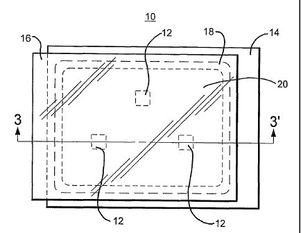
bonded to first substrate 32 in order to seal the chamber 21. As illustrated,
second
substrate has a dome-like shape and includes a peripheral shoulder 76 and rim
77 for
engaging the edges of first substrate 32. Electrical connections to radiation
emitter(s) 12
may extend through vias formed in first substrate 32 that extend from an inner
surface to
an outer surface thereof. The chamber 21 may be filled with the second
substrate
inverted and prior to ultrasonic welding. Alternatively, a fill hole may be
provided
through first substrate so that the chamber may be filled after welding. A UV
curable or
other plug may then be used to seal the fill hole.
[0083] Fig. 7 shows a fifth embodiment of the present invention. In this fifth
embodiment, a reflective mask 80 is provided on a surface of second substrate
16. The
reflective mask 80 includes a plurality of non-masked openings 82 above each
radiation
emitter 12. Mask 80 may optionally include a small reflective spot 84 directly
over each
emitter 12 so as to prevent light from directly emitting from an emitter 12
through mask
80. In this manner, emitters that emit light of different colors may be
disposed within
-22-
CA 02432286 2003-06-18
WO 02/061805 PCT/US02/03161
the chamber 21, and the light emitted from the emitters will mix within the
chamber 21
prior to being emitted from the assembly. Mask 80 may be a patterned
reflective or
diffuse coating or a filter and be made integral with patterned conductors if
used.
Patterns other than those shown may be used to optimize various optical
qualities
without departing from the scope of the invention.
[0084] Figs. 15 and 16 show yet another embodiment of the present invention.
As
shown in the cross sectional view of Fig. 15, radiation emitted from emitters
12 is either
nearly completely transmitted, partially transmitted and partially internally
reflected, or
nearly completely internally reflected from second substrate 16 depending upon
the angle
at which the radiation strikes the surfaces of second substrate 16. Whether
radiation
(i. e. , a light ray) is internally reflected depends upon whether the light
ray strikes the
surface at an angle that is greater than the critical angle as determined by
application of
Fresnel's equations and Snell's Laws. If the entire upper surface of first
substrate 14
served as a specular reflector, those light rays T that are totally internally
reflected from
a surface of second substrate 16 would continue to be totally internally
reflected from the
upper surface of first substrate 14 and then again from the surfaces of second
substrate
16. To cause the light rays T that would otherwise be totally internally
reflected, to
ultimately exit through the second substrate of the radiation emitting device,
upper
surface of first substrate 14 may have different reflective zones--namely, a
specularly
reflective zone 301 and a diffuse reflective zone 303. As shown in Figs. 15
and 16,
separate specularly reflective zones 301 are provided for each emitter 12 and
are circular
in shape with the associated emitter 12 disposed in the center of the circle.
The
remainder of the upper surface of first substrate 14 (with the exception of
that area
covered by electrical traces and contact terminals) constitutes the diffuse
reflective zone
303. Specular reflective zones 301 may be provided as a portion of the
patterned
electrical conductor traces 304. As will be apparent to those skilled in the
art, the
diameter of the circular specular reflection zone 301 is selected to be small
enough not to
reflect light rays that are totally internally reflected from a surface of the
second
substrate 16, and yet large enough to reflect all other light. The diffuse
reflective zone
303 is provided to diffuse those light rays T that are totally internally
reflected from a
surface of the second substrate 16 and thereby reflect the light at angles
that are likely to
allow the light to exit the second substrate 16. Diffusely reflective zone 303
may have a
coating including a photoluminescent material.
-23-
CA 02432286 2003-06-18
WO 02/061805 PCT/US02/03161
[0085] While specular reflection zones 301 are shown as being circular on a
planar
surface, it will be appreciated that the first substrate 14 may include
recessed reflective
cups. Figs. 17A and 17B show alternate variations of such a construction.
Specifically,
Fig. 17A shows the use of reflective partitions 311 between radiation emitters
12 so as to
divert those light rays that would otherwise strike a surface of second
substrate 16 at an
angle exceeding the critical angle. Reflective partitions may form a parabolic
reflective
cup or other shaped cup and may be specular or diffuse in surface character.
Fig. 17B
shows a variation of the structure shown in Fig. 17A in which reflective
partitions 313
are integrally formed in the upper surface of first substrate 315. Note that
partitions 311
and 313 in the above embodiments may function as a spacer between the first
and second
substrates.
[0086] Fig. 8 shows a vehicle headlamp 2600 constructed in accordance with the
present
invention. As shown, the headlamp includes a light emitting assembly similar
to those
shown above, except that it includes an array of radiation emitters 2603 and
2605 within
the sealed chamber 21 that is formed between a first substrate 2601, a second
substrate
2630, and a seal (not shown). Second substrate 2630 preferably includes a
plurality of
micro-lenses 2631 formed in its outer surface above each one or each group of
emitters
2603, 2605. First substrate 2601 preferably includes a heat extraction member
2621 and
a plurality of reflective cups 2602 and 2605 in which each one or each group
of emitters
are mounted. Emitters 2603 are connected to electrical conductor strip 2607
through a
wire bond 2609 and a resistor 2611. Emitters 2605 are connected to electrical
conductor
strip 2613 through a bonding wire 2615 and a resistor 2617. A second assembly
similar
to that shown in Fig. 8 may also be disposed in a common headlamp housing and
preferably disposed at an angle relative to the first assembly so as to
produce high
beams. By utilizing the high power light emitting assembly of the present
invention,
vehicle headlamps may be constructed that require fewer LEDs or other emitters
to
produce the requisite illumination levels that are expected for vehicles.
Headlamp 2600
may also be a fog lamp or other lamp assembly.
[0087] Fig. 9 shows an examplary circuit 100 that may be used in the above
embodiments of the present invention. As shown, three external connections are
provided including a ground contact 102, a first supply voltage contact 104,
and a
second supply voltage contact 106. Second supply voltage contact is provided
to enable
a bias voltage to be applied between a first LED 110, and two second LEDs 112
via a
-24-
CA 02432286 2003-06-18
WO 02/061805 PCT/US02/03161
resistor 114, and thereby adjust the relative intensity of the second LEDs
relative to the
first LED, which is particularly advantageous when the first and second LEDs
emit light
of different colors. A resistor 118 is coupled between the first LED and first
supply
voltage contact. Resistor 118, first LED 110, and second LEDs 112 are coupled
in
series between first supply voltage contact 104 and ground contact 102. As
shown in
Fig. 9, a plurality of such series-connected LEDs may be connected in
parallel. Portions
of circuit 100 may be printed on one or both of substrates 14 and 16. Portions
of circuit
100 may be disposed inside or outside of the sealed chamber 21, with contacts
102, 104,
and 106 extending out of the chamber for external connection. Resistors 114
and 118
may likewise be provided outside of the chamber to lower the heat generated
inside the
chamber.
[0088] In a preferred embodiment, LEDs 110 emit blue-green light while LEDs
112
emit amber light. With such an arrangement, effective white light may be
emitted from
the assembly.
[0089] Fig. 10 shows an initial subassembly that forms a part of the final
assembly
shown in Fig. 11 in accordance with a sixth embodiment of the present
invention. The
package 150 includes a printed circuit board 155, which in the example
provided below,
is made of BeO. Various electrically conductive traces are formed on circuit
board 155.
In the example shown in Figs. 10 and 11, a first trace 160 extends from a
first electrical
contact 162 to a first terminal of each of four first resistors 164a-164d.
Traces 166a-
166b extend from a second terminal of respective resistors 164a-164d to a
respective
anode of a corresponding pad 168a-168d upon which is mounted a first set of
LEDs
170a-170d. First LEDs 170a-170d are mounted with their anode in electrical
contact
with pads 168a-168d, respectively. Traces 166a-166d also extend to a position
proximate pads 172a-172d upon which are mounted respective second LEDs 174a-
174d.
Second LEDs are mounted with their anodes in electrical contact with pads 172a-
172d.
Wire bonds 176a-176d electrically couple the cathodes of second LEDs 174a-174d
to the
end of trace 166.
[0090] The cathodes of first LEDs 170a-170d are electrically coupled via
corresponding
wire bonds 178a-178d to a respective trace 180a-180d, which in turn are
coupled to
respective first terminals of second resistors 182a-182d. Second terminals of
resistors
182a-182d, in turn, are commonly coupled to a trace 184, which extends and is
-25-
CA 02432286 2003-06-18
WO 02/061805 PCT/US02/03161
electrically coupled to a second contact terminal 186. The resistors 164a-164d
and 182a-
182d are preferably 2 Q, 1 W thick film resistors that are printed on circuit
board 155.
[0091] Pads 172a-172b, to which the anodes of second LEDs 174a-174d are
respectively
coupled, are electrically coupled to respective traces 188a-188d. Each of
these traces
188a-188d is connected by means of a respective wire bond 190a-190d to another
respective trace 192a-192d on the opposite side of trace 184. Traces 192a-192d
are
respectively coupled to cathodes of respective third LEDs 194a-194d by a wire
bond
196a-196d. The anodes of third LEDs 194a-194d are mounted on corresponding
pads
198a-198d, which in turn are commonly coupled together via a trace 200 that
extends
and is electrically coupled to a third contact terminal 202.
[0092] With the circuit layout as shown in Fig. 10, the resulting circuit has
a schematic
corresponding generally to Fig. 9, where first LEDs 170a-170d correspond to
LEDs
110, second and third LEDs 174a-174d and 194a-194d correspond to LEDs 112,
first
resistors 164a-164d correspond to resistors 114, and second resistors 182a-
182d
correspond to resistors 118.
[0093] In a preferred embodiment and in the example discussed below, first
LEDs 170a-
170d are preferably InGaN LED chips that emit blue-green light. Botli the
second and
third LEDs 174a-174d and 194a-194d are AlInGaP LED chips that emit amber
light. By
utilizing these LED chips, effective white light may be emitted from the
package in
accordance with the teachings of U.S. Patent No. 5,803,579 entitled
"ILLUMINATOR
ASSEMBLY INCORPORATING LIGHT EMITTING DIODES" by Robert R. Turnbull
et al.
[0094] Once the above-described circuit has been constructed, a cover glass
205 is
attached to circuit board 155 with an epoxy seal 210, which encircles the
circuit
components, with the exception of electrical contacts 162, 186, and 202 and
with the
exception of a small hole through which the resultant sealed chamber 21 may be
filled
with a liquid or gel. In the example discussed below, the seal chamber was
filed with
Galden D02TS. Subsequently, the hole provided in the epoxy between cover 205
and
circuit board 155 was plugged with a plug 212 made of Dynax UV cure adhesive.
The
resultant structure is shown in Fig. 11.
[0095] As apparent from Fig. 11, the resultant final package assembly includes
three
contact pads 162, 186, and 202, which extend outward from the sealed chamber
21 and
up to the edge of printed circuit board 155. In this manner, a conventional
low insertion
-26-
CA 02432286 2003-06-18
WO 02/061805 PCT/US02/03161
force edge connector may be connected to the contact pads for coupling to the
drive
circuit. Such an edge connector may be a conventional PCI or ISA slot
connector. It
should be understood that another number of contact pads may be used,
dependent on
the electrical configuration used.
[0096] The invention will be further clarified by the following example, which
is
intended to be exemplary of the invention and are not intended in any manner
to limit the
invention.
EXAMPLE
[0097] To demonstrate the effectiveness of the present invention, a package
assembly
was constructed as illustrated in Figs. 10 and 11 and described above. The
structure had
a length of approximately 1.5 inches and a width of approximately 1.5 inches,
with the
external contact pads being approximately 0.25 inch long. To demonstrate the
effectiveness of the present invention, the illumination from the device was
measured at
various power levels prior to filling the sealed chamber 21 with any liquid.
Then, the
assembly was filled with liquid and plugged and the illuminance was again
measured at
the same power levels. The results of these measurements are illustrated in
Fig. 12,
with the illuminance measured in foot-candles at 18 inches. As apparent from
Fig. 12,
the provision of the liquid in physical and thermal contact with the LEDs
improved their
performance markedly. The improvement increased as the applied power
increased. It
should be understood that, for this sample, increased illuminance at each
indicated
power level for the filled radiation emitter relative to the unfilled
radiation emitter is an
indication of reduced junction operating temperature and reduced assembly
thermal
resistance.
[0098] Fig. 13 is a plot of the relative spectral irradiance as a function of
wavelength
with the chamber 21 of the device not filled with any liquid. The relative
spectral
irradiance was measured at five different power levels. Subsequently, after
the device
was filled with liquid, the same plots were obtained and are illustrated in
Fig. 14.
[0099] While the above invention has been described with respect to the
provision of
optical radiation emitters and other radiation emitting devices within a
sealed chamber 21
of the inventive package, the inventive package may similarly be used to
improve the
heat dissipation from other electronic components. For example, as shown in
Fig. 18, a
microprocessor 230, a sensor 240, a resistor 245, and other electronic
components,
particularly other semiconductor electronic components, may be disposed within
sealed
-27-
CA 02432286 2003-06-18
WO 02/061805 PCT/US02/03161
chamber 250 that is formed between two members 255 and 260. Examples of other
electronic components that could desirably be placed in the sealed chamber
either alone
or in combination with radiation emitters, microprocessors, resistors, sensors
or other
components, including thermistors, diodes, Zener diodes, photodiodes,
transistors,
voltage regulators, Peltier effect diodes or other thermoelectric cooling
chips or
materials, phototransistors, etc. Members 255 and 260 may have any of the
constructions discussed above. However, if none of the components within the
sealed
chamber are optical components, both members 255 and 260 may be opaque.
Without
such a constraint, first member 255 may, for example, be a printed circuit
board while
second member 260 may be a heat sink, preferably made of a highly thermally
conductive material and having a large surface area. Such a large surface area
may be
provided by including various fins 262 extending outward away from the sealed
chamber. As also shown in Fig. 18, various passageways 264 may be provided
through
heat sink member 260 through which liquid may flow. These passages may join
into
sealed chamber 250 to allow the liquid contained therein to flow through the
passageways to expedite heat dissipation from the liquid.
[0100] The electronic components mounted in the chamber may be surface mount
(SMT), through-hole (THD), ball grid array (BGA), chip-on-board, chip-on-
glass, or
other common semiconductor device form. Electrical connections to/from/between
these components, and any patterned conductors within the chamber or to
contacts
exiting the chamber, may be solder, solder bump, solder paste, conductive
epoxy,
eutectic attach, wire bond, leadframe, or other electrical connection means.
[0101] Another alternative embodiment would enable both members 255 and 260 to
be
printed circuit boards that are sandwiched together by an epoxy seal and
filled with a
liquid or gel. This may enable heat dissipation in accordance with the present
invention
from circuit components mounted to either or both of the circuit boards.
[0102] It should also be appreciated that the components shown in Fig. 18 may
be
combined with a radiation emitter as in the other embodiments within a single
sealed
chamber. It may, for example, be beneficial to include resistors and/or a
sensor within
the same sealed chamber as the radiation emitters. Such a sensor may be a
thermal
sensor, such as a thermistor, so as to provide a mechanism for monitoring the
temperature of the liquid within the sealed chamber and for enabling the
current
provided to the LED chips to be controlled as a function of the temperature
within the
-28-
CA 02432286 2006-11-07
chamber. This would allow the LED chips to be driven at their maximum safe
Ievel.- It
may also be desirable to include a voltage regulator to regulate the
electrical drive signal
to any electroluminescent radiation sources in the chamber. Additionally, it
may be
desirable to include any one or conlbination of transistors, phototransistors,
diodes,
photodiodes, or Zener diodes in the sealed chamber.
[0103] It may further be desirable to dispose an optical sensor within the
same
sealed chamber as the radiation eniitters. U.S. Patent No. 6,498,440, issued
December 24, 2002, entitled "LAMP ASSEMBLY INCORPORATING OPTICAL
FEEDBACK," to Joseph S. Stam et al. discloses the advantages of utilizing an
optical sensor in combination with a plurality of LED chips. Such sensors may
be
employed for many purposes such as to provide feed back for the control of
electroluminescent emitters 12 in the device. In the event an optical sensor
is
provided in the sealed chamber, it may be desirable to incorporate light
absorbing
materials within the sealed chamber so as to effectively filter the light that
reaches
the sensor.
[0104] The radiation emitter device described herein can be used to provide a
near IR
night vision system for use in autonlobiles and other applications. A
radiation emitter
device is constructed as describecl above using IR LED die emitting radiation
at a
wavelength longer than the human eye can detect but still within the sensing
capability of
an electronic image sensor. Preferably, this wavelength range is between 800
and 880
nm, but may be as low as 700 nni or as high as 1200 nm. Such IR-emitting LED
die are
available from Tyntec Corporation of Hsinchu, Taiwan.
[0105] Current vehicular night vision systems have several disadvantages which
are
overcome by using a near IR night vision system. Current systems sense far IR
radiation - essentially heat. Detectors which sense far IR radiation are
significantly
more expensive than detectors wliich sense near IR radiation. Additionally,
glass is
opaque to far IR radiation thus mandating that the sensor be placed outside of
the
vehicle's cabin thereby subjecting the system to much harsher environmental
conditions.
Also, glass optics cannot be used and more expensive optical materials
transparent to far
IR radiation must be used instead. Finally, objects which are not at a higher
temperature
than the ambient surroundings are not sensed as well as hot objects.
Therefore, it is
-29-
CA 02432286 2003-06-18
WO 02/061805 PCT/US02/03161
possible to have an object in the road which is not adequately detected by a
far IR
system.
[0106] The radiation emitter device of the current invention may thus be
configured to
emit radiation illuminating the scene imaged by the camera. In an automobile,
the IR
illuminator assemblies may be packaged with or near the vehicle's headlamps.
Since IR
radiation is not detectable to the human eye, it is possible to substantially
illuminate the
scene in front of a vehicle without any concern for glare disrupting oncoming
or
preceding drivers.
[0107] The camera is configured to image at least the same spectra of light as
the IR
LEDs emit. Preferably, the camera's spectral sensitivity is limited by the use
of filters
to only the wavelength range of light emitted by the IR LEDs. This reduces any
washing-out or blooming in the image from other light sources. The camera can
be
mounted to look through the vehicle's windshield in the region cleaned by the
vehicle's
wiper and washer system by placing the camera in the mount of a rearview
mirror. The
camera preferably uses a wide dynamic image sensor to allow for imaging of
both bright
and faint objects in the forward scene simultaneously. Such an image sensor is
described in commonly-assigned U.S. Patent No. 6,008,486 entitled "WIDE
DYNAMIC RANGE OPTICAL SENSOR."
[0108] If a scene rearward of the vehicle is to be imaged using such a near IR
imaging
system, the camera may be mounted in the center high-mounted stop lamp (CHMSL)
in
a tail liglit, or behind the rear window, while the radiation emitting device
of the present
invention may be mounted in the same location as the camera or in a different
one of the
above locations. A similar rear vision system is disclosed in commonly
assigned PCT
International Publication No. WO 00/15462, entitled "SYSTEMS AND
COMPONENTS FOR ENHANCING REAR VISION FROM A VEHICLE," by
Frederick T. Bauer et al.
[0109] As will be appreciated by those skilled in the art, the radiation
emitting device of
the present invention allows for more efficient extraction of the heat
generated by the
radiation emitters. This improved extraction allows for a greater driving
current to be
delivered to the radiation emitters, which, in turn, generates higher
radiation flux levels
than previously obtained. The LED construction disclosed in the commonly-
assigned
U.S. Patent No. 6,335,548 discussed above, achieves power densities of up to
about 2
W/in2 or more while the structure of the present invention may obtain power
densities of
-30-
CA 02432286 2003-06-18
WO 02/061805 PCT/US02/03161
up to 5 to 10 W/in2 or more. Certain embodiments of the present invention may
be
capable of power dissipation in excess of 1 W for miniature lamp applications
(i.e.,
small area embodiments), and up to and exceeding 1000 W for high power lamp
applications (i.e., large area embodiments).
[0110] Additionally, the likelihood that any wire bonds utilized may fatigue
or break is
either eliminated (as in the case with the first embodiment where wire bonds
are not
required), or significantly reduced, since the present invention does not
encapsulate these
wire bonds with a solid encapsulant. Because the wire bonds used in the
embodiment
shown in Figs. 4 and 5 are surrounded by a liquid or gel, shear forces cannot
be
transferred to the wire bond as a result of any thermal expansion or
contraction as would
be the case if they were encapsulated in a conventional encapsulant material.
[0111] A manufacturing process for making embodiments of the present invention
comprising light engine modules first includes mounting optional surface
mount, BGA,
chips or other electronic components onto the first substrate. Next, one or
more LED
chips to the first substrate using eutectic attachment, solder attachment, die-
attach
adhesive, epoxy or the like. Next, additional optional surface mount, BGA,
chips or
other electronic components may be mounted onto first substrate. A curing
stage or
reflow stage is typically performed, as appropriate to form permanent
electrical and
mechanical bonds between chips and components and the first substrate. Next,
wirebonding is performed for embodiments using wirebonds for electrical
connection to
one or more LED or electronic component chip. Next, a barrier adhesive, seal
or gasket
material is placed or dispensed onto first or second substrate. The seal
material can
optionally or additionally be pre-arranged upon or made integral with portions
of either
first or second substrate. At any point up to this point in the process,
optional spacers
may be placed within the region subsequently forming the cavity, either by
placing or
mounting them on the first substrate or the second substrate or by sandwiching
them
between the two substrates. Next, the first and second substrates are placed
in close
proximity such that any seal material or structure bridges the narrow gap
between them
along an appropriate portion of their surfaces. To facilitate large scale
manufacturing
and production of several modules at one time or modules having several semi-
independent chambers, several first substrates may be placed onto one second
substrate
(and associated seal material) or vice versa. Seal material is next cured,
sintered, or
melted by thermal treatment or radiation exposure such as baking, IR heating,
e-beam or
-31-
CA 02432286 2003-06-18
WO 02/061805 PCT/US02/03161
microwave curing, reflow or other similar process. Small openings may be left
within
first or second substrate or seal material to provide a channel for subsequent
filling of
the cavity. Fluid may then be introduced into the cavity by vacuum-backfill
process, 2-
port pressure or gravity filling or other means. After the cavity is filled,
openings in the
first or second substrate or seal may be plugged with UV curable epoxy or
other
sealant/barrier material.
[0112] The above description is considered that of the preferred embodiments
only.
Modifications of the invention will occur to those skilled in the art and to
those who
make or use the invention. Therefore, it is understood that the embodiments
shown in
the drawings and described above are merely for illustrative purposes and not
intended
to limit the scope of the invention, which is defined by the following claims
as
interpreted according to the principles of patent law, including the doctrine
of
equivalents.
-32-