Note: Descriptions are shown in the official language in which they were submitted.
CA 02432300 2009-06-03
1
SECONDUCTOR WAFER PROCESSING TO INCREASE THE USABLE
PLANAR SURFACE AREA
FIELD OF THE INVENTION
The present invention relates to semiconductor processing, and in particular
to
methods for processing a semiconductor wafer to increase the useable planar
surface area,
to a method for fabricating solar cells and to a process for decreasing the
reflectivity of a
semiconductor surface.
BACKGROUND
In most areas of semiconductor processing, the cost of the starting substrate
wafer is small compared to the value of the final, processed wafer. However,
this is not
always the case. For example, the photovoltaic solar cell industry is
extremely cost
sensitive, and the cost of a starting silicon wafer is typically nearly half
of the processed
wafer value. Thus, in this industry it is extremely important that the silicon
substrates are
used as efficiently as possible. These substrates are produced by sawing thin
slices from
a cylindrical boule of crystalline silicon, typically 6 inches (about l5cm) in
diameter. The
thinnest slice that can be cut is determined by the mechanical properties of
the silicon,
and is typically 300 - 400 m for the current generation of 6 inch wafers, but
is projected
to be 200 pm for the next wafer generation. However, the kerf loss for sawing
through a
6 inch wafer is approximately 250 m, meaning that much of the boule ends up
as
powder. There is a need, therefore, for a method which increases the useful
surface area
of semiconductor for a given unit volume of the semiconductor, or at least for
a useful
alternative to current methods of semiconductor processing.
SUMMARY OF THE INVENTION
In accordance with one embodiment of the present invention, there is
provided a process for increasing the usable surface area of a semiconductor
wafer
having a substantially planar surface and a thickness dimension at right
angles to
the substantially planar surface, the process comprising the steps of:
CA 02432300 2009-06-03
2
a) selecting a strip thickness and a slot width for division of the wafer into
a plurality of adjoining strips such that the thickness of the wafer is
greater than the
sum of the strip thickness and the slot width,
b) selecting a technique for forming a plurality of slots, each slot having
the slot width, and thereby forming the plurality of adjoining strips in the
wafer with
each strip having the strip thickness, wherein each of the slots when formed
extend
from the planar surface at an angle thereto and the slots extending through
70% or
more of the thickness of the wafer over either all of the slot length or most
of the
slot length; and
c) processing a portion of the wafer into the plurality of adjoining strips
using the selected technique wherein the adjoining strips are supported within
a
frame.
In another embodiment, the present invention provides a process for
increasing the usable surface area of a semiconductor wafer having a planar
surface and a thickness dimension at right angles to the planar surface, the
process
comprising the steps of:
a) selecting a strip thickness and a slot width for division of the wafer
into a plurality of adjoining strips such that the thickness of the wafer is
greater than
the sum of the strip thickness and the slot width,
b) selecting a technique for forming a plurality of slots, each slot
having the slot width, and thereby forming the plurality of adjoining strips
in the
wafer with each strip having the strip thickness, wherein each of the slots
when
formed extend from the substantially planar surface at an angle thereto and
the
slots extending either through the wafer or nearly through the wafer over
either all
of the slot length or most of the slot length; and
c) processing a portion of the wafer into the plurality of adjoining strips
using the selected technique wherein the adjoining strips are connected by
multiple
interconnecting portions.
CA 02432300 2009-06-03
3
The semiconductor wafer is typically single crystal silicon or
multicrystalline
silicon. However, the semiconductor wafer may be a wafer of other
semiconductor
material capable of being fabricated into a thin, substantially flat wafer.
The strips may be at any angle to the surface of the semiconductor wafer or
substrate, such as at an angle of from 5 to 90 to the surface of the wafer
or
substrate. Typically the strips are at an angle of at least 300, more
typically at least
45 , still more typically at least 60 and even more typically about 90 (that
is,
substantially perpendicular) to the surface of the wafer or substrate.
A laser may be used to form the slots in the wafer. An area around the
periphery of the wafer may be left uncut, forming a frame, so that all the
resulting
strips are held within the frame. This allows handling of the wafer following
formation of the slots, while the strips undergo further processing. The
strips may
be separated from the frame at any convenient stage of the further processing.
A dicing saw may be used to form the slots in the wafer. An area around the
periphery of the wafer may be left uncut, forming a frame, so that all the
resulting
strips are held within the frame. This allows handling of the wafer following
formation of the slots, while the strips undergo further processing. The
strips may
be separated from the frame at any convenient stage of the further processing.
In yet another form of the processes of the embodiments of the invention,
wet anisotropic etching of (110) oriented wafers is used to form the slots. An
area
around the periphery of the wafer may be left unetched, forming a frame, so
that all
the resulting strips are held within the frame. This allows handling of the
wafer
following formation of the slots, while the strips undergo further processing.
The
strips may be separated from the frame at any convenient stage of the further
processing.
CA 02432300 2009-06-03
3a
In still another form of the processes of the embodiments of the invention,
photo-electrochemical etching may be used to create an aligned series of
perforations through a semiconductor wafer, and chemical etching may then be
used to etch through the semiconductor remaining between the perforations and
along the lines defined by the perforations, to form a narrow slot through the
wafer.
CA 02432300 2008-01-15
4
In a further form of the processes of the embodiments of the invention,
at least one interconnecting portion is formed in or on the wafer, which
connects adjoining strips to each other to maintain a relatively constant gap
between the
strips. Usually, in this form of the methods of the invention, there are a
plurality of
interconnecting strips. Conveniently, the interconnecting strips are spaced
apart at regular
intervals along the length of the strips. The inclusion of such
interconnecting portions
allows processing steps such as diffusions and oxidations to be carried out in
a reliable
and repeatable manner, resulting in predictable diffusion profiles and oxide
thicknesses
down the sides of the slots. The interconnecting portions suitably take the
form of one or
more strips of the semiconductor material formed at least partly across one or
both main
surfaces thereof, perpendicular or oblique to, and usually substantially
perpendicular to,
the strips which are defined by the plurality of slots.
The methods described herein are equally applicable to entire semiconductor
wafers and to pieces of wafers. Consequently, the word wafer used in this
specification is
to be taken to refer to entire wafers or portions thereof
In the embodiments of the invention the slots are typically created
through the complete thickness of the wafer, though not necessarily.
Where the slots are created through the thickness of the wafer, they may be
created in one
step or more than one step. For example, the plurality of slots may be created
partly
through the wafer, optionally further processing may be carried out, such as
doping of the
surfaces of the strips so created, and then the plurality of slots may be
completed by
cutting or etching through the remainder of the thickness of the wafer. Thus,
the step of
separating the strips from each other will typically occur when the creation
of the slots is
completed through the entire thickness of the wafer. Alternatively, if a frame
is left uncut
around the periphery of the wafer as described above, the step of separating
the strips
from each other will occur when the strips are cut from the frame. As a
further
possibility, when interconnecting portions are employed to connect adjoining
strips, as
described above, the step of separating the strips from each other occurs when
the
interconnecting portions are removed or broken. As a still further possibility
(though less
preferred) the strips may be separated from each other by breaking them apart
if the slots
CA 02432300 2008-01-15
between the strips are formed only partway though the wafer but the remaining
part of the
wafer at the bottom of the slots is very thin.
Preferably, most of the processing of the strips into solar cells is carried
out
while the strips are supported within a frame formed from an uncut area around
the
periphery of the wafer. Following processing, the strips are cut out of the
frame and laid
flat side by side. Preferably, separation of the strips from the frame is
carried out using a
laser or dicing saw.
Advantageously, solar cells made by a process which includes a method in
accordance with the present invention may be arranged with gaps between
adjacent cells
and used with an optical concentrator to increase the effective solar cell
area.
Advantageously, said solar cells may be used with optical reflectors in order
to
utilise the cells fabricated by illumination on both sides of each solar cell
strip.
In some forms of the methods of the invention, such as when chemical etching
is
used to form the slots that separate the strips, the newly-exposed surface of
the
semiconductor material is a polished surface. - Such a surface is typically a
reflective
surface, and it will be appreciated that a reflective surface is undesirable
for a solar cell.
Although some techniques exist for texturing a polished semiconductor surface,
they are
not well adapted to be used in conjunction with the methods of the first to
third
embodiments of the present invention.
CA 02432300 2008-01-15
6
BRIEF DESCRIPTION OF THE DRAWINGS
Preferred embodiments of the present invention are hereinafter described, by
way of ex=plc only, with reference to the accompanying drawings, which are
briefly
described as follows.
Figure 1 is a schematic diagram showing top (Figure 1(a)) and cross sectional
(Figure 1(b)) views of a silicon wafer following the formation of slots
according to a
preferred embodiment.
CA 02432300 2003-05-28
WO 02/45143 PCT/AUO1/01546
7
Figure 2(a) shows a top view and a cross sectional view of a silicon wafer in
which macropores are formed according to a further embodiment of the
invention; Figure
2(b) shows a top view of the silicon wafer illustrated in Figure 2(a) after
grooves have
been formed by joining the macropores.
Figure 3 is a schematic diagram showing bottom (Figure 3(a)) and cross-
sectional (Figure 3(b)) views of a silicon wafer following the formation of
slots and
interconnecting strips according to a preferred embodiment.
Figure 4 is a schematic diagram showing top (Figure 4(a)) and cross-sectional
(Figure 4(b)) views of a silicon wafer following the formation of shallow
trenches
io according to a preferred embodiment.
Figure 5 is a schematic diagram showing a top view of the structure resulting
from the formation of slots in the wafer shown in Figure 4, in accordance with
a preferred
embodiment.
Figure 6(a) is a schematic cross sectional view of a silicon wafer into which
a
plurality of shallow grooves has been formed. Figure 6(b) is a schematic cross
sectional
view of the same structure after etching, orthogonal o the cross-section shown
in Figure
6(a).
Figure 7 is a top view of the structure illustrated in Figure 6(b).
Figures 8(a) and 8(b) are schematic cross sectional views of a part of a (110)
oriented silicon wafer before and after the formation of slots in the wafer.
Figure 8(c) is a
schematic top view of the structure shown in cross-section in Figure 8(b).
Figure 9 is a schematic diagram illustrating a method for separating silicon
strips
from their frame by means of a laser, in accordance with a preferred
embodiment.
Figure 10 is a schematic diagram showing a cross-sectional view of a silicon
strip prepared in accordance with the present invention and fabricated into a
solar cell.
Figure 11 is a schematic diagram showing a cross-sectional view of a silicon
strip prepared in accordance with the present invention and fabricated into
another solar
cell.
Figures 12(a), 12(b) and 12(c) are a series of schematic diagrams showing
cross-
sectional views of the front and rear surfaces of a silicon wafer during a
strip formation
process of a preferred embodiment.
Figures 13(a) to 13(d) are schematic illustrations of various ways in which
silicon strips prepared by the process of the present invention can be
electrically
interconnected.
CA 02432300 2003-05-28
WO 02/45143 PCT/AUO1/01546
8
Figure 14 is a schematic diagram showing a cross-sectional view of silicon
strips
mounted on a suitable substrate and positioned adjacent to a light
concentrator to
concentrate sunlight onto the strips.
Figure 15 is a schematic diagram showing a cross-sectional view of silicon
strips
mounted on a suitable substrate and positioned adjacent to another light
concentrator to
concentrate sunlight onto the strips.
Figure 16 is a schematic diagram showing a cross-sectional view of silicon
strips
mounted on a suitable substrate and positioned adjacent to another light
concentrator to
concentrate sunlight onto the strips.
Figure 17 is a schematic diagram of a silicon strip following surface
texturing as
described herein.
DETAILED DESCRIPTION OF THE PREFERRED EMBODIMENT AND
OTHER EMBODIMENTS
In the description of the drawings which follows, like items are referred to
by
reference to like numerals. It will be appreciated that the drawings are not
to scale and
are diagrammatic only. For example, for greater clarity, the drawings do not
necessarily
depict all of the slots, strips, interconnecting portions and the like formed
in a
semiconductor material by the methods described.
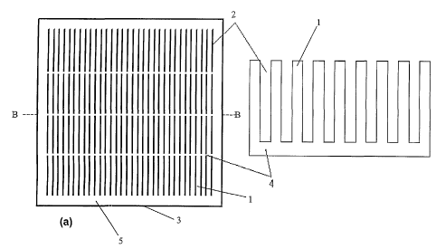
Referring to Figure 1(a), a silicon wafer 3, at least 0.5mm thick and
typically
about lmm thick, is formed by standard crystal growth and wafering techniques.
Wafer 3
is preferably single-crystal, although multi-crystalline wafers may also be
used. A series
of parallel channels or slots 2 is formed in wafer 3, with the slots being
typically 0.05mm
wide and the pitch of the slots being typically 0.1mm, forming thin parallel
strips of
silicon 1, about 0.05mm wide. Because slots 2 do not extend all the way to the
edges of
wafer 3, a frame 5 of uncut silicon holds strips 1 in place. Frame 5 is
typically 5mm wide
on each side.
Slots 2 can be formed by cutting the wafer with a dicing saw having a narrow
blade. Alternatively, slots 2 can be formed by laser ablation. For example, a
Resonetics
Nd:YLF Q-switched laser operating at the fundamental wavelength of 1046iun or
frequency doubled (523nm) can be used to cut wafer 3. Other systems can also
be used,
such as a water jet guided laser cutting system as described in United States
patent no.
5,773,791. As a further possibility, slots 2 can be formed by using a wet
anisotropic
etchant, such as potassium hydroxide solution (KOH), as is well known in the
art. In this
case, it is necessary to use a single-crystal silicon wafer of (110)
orientation. First, a
CA 02432300 2003-05-28
WO 02/45143 PCT/AUO1/01546
9
suitable etch mask such as silicon dioxide or silicon nitride is deposited or
grown on both
sides of wafer 3. Photolithography is used to open narrow stripes in the etch
mask on one
surface of wafer 3, the stripes being typically 0.005mm wide, at a 0.lmm pitch
and
oriented along the [1 -1 -2] direction. Wafer 3 is now immersed in the etching
solution.
One suitable solution is an aqueous solution of 44% w/v KOH, with etching done
at or
above room temperature.
Any of the methods described above can be carried out either from one side of
wafer 3 only, or from both sides of wafer 3, allowing thicker wafers to be
used. For
example, when using a laser capable of ablating 0.5mm of silicon, a first set
of slots is
io made from the front side of a Imm thick wafer. The wafer is then turned
around, and a
second set of slots, aligned to the first, is made. Alternatively, both sets
of slots may be
formed simultaneously by having aligned laser beams above and below the
sample.
If either a dicing saw or a laser is used to form the slots, it is desirable
to have
multiple blades or multiple beams cutting slots into the substrate
simultaneously in order
to speed up the process. For example, if slots are to be formed over a
1Ox10cm2 wafer of
silicon with a pitch of 0.lmm, one thousand cuts are required. If twenty laser
beams are
arranged to hit the sample surface at a pitch of 5mm, each beam is required to
make only
fifty cuts.
In Figure 1(b) there is shown an enlarged vertical cross-section through the
wafer 3 along line A-A showing strips 1 and spaces 2 in cross-sectional view.
Figures 2(a) and 2(b) illustrate a further method of forming slots in the
substrate
by use of photo-electrochemical etching. Photo-electrochemical etching is
described by
Lehmann (Journal of the Electrochemical Society, Vol. 140, No. 10, (1993)
p.2836). As
shown in Figure 2(a), an n type silicon wafer 3 of (100) orientation is used.
Wafer 3 is
provided with an array of indents 26 by lithography and KOH etching. Indents
26 are
arranged along rows, with the spacing between indents 26 being typically 5-10
microns,
while the spacing between rows of indents 26 is typically 50 microns. Wafer 3
is then
immersed in a suitable etch, such as a 10% solution of hydrofluoric acid.
Illumination 65
is directed onto the rear of wafer 3 and a positive bias voltage is applied to
wafer 3. A
counterelectrode 28 is placed in the solution in the vicinity of the wafer.
Under these
conditions, an array of macropores 27 is formed which extends into silicon
wafer 3.
Etching is continued until macropores 27 extend all the way through wafer 3.
Silicon wafer 3, provided with an array of macropores 27, is then immersed in
a
silicon etchant such as a potassium hydroxide solution. This results in an
enlargement of
CA 02432300 2003-05-28
WO 02/45143 PCT/AUO1/01546
macropores 27. As shown in Figure 2(b), with continued etching, macropores 27
coalesce to form slots 2 extending through wafer 3. This technique allows the
creation of
very narrow slots 2 of less than 10 microns in width.
In yet a further form of the methods of the first to third embodiments, slots
5 through the wafer extend all the way through the wafer over most of their
length but at
regular intervals along the slots they are less deep so that some substrate
remains at the
bottom of the groove, forming a series of connecting strips. This is shown in
Figure 3(a)
and 3(b). Figure 3(a) is a view from the underside of the wafer showing
connecting strips
4 running across wafer 3 from opposite sides of frame 5, with slots 2
extending through
10 wafer 3 over most of their length. Figure 3(b) is a vertical cross-section
through line B-B
in Figure 3(a). The structure shown in Figures 3(a) and 3(b) can be fabricated
by laser
ablation. Connecting strips 4 restrict the amount of bending of silicon strips
1 during
further processing and thereby limit the variation in slot width. This ensures
that the
sidewalls of strips 1 can be reliably processed, as described below.
Connecting strips 4
are typically 0.lmm wide, 0.05mm high and spaced 10mm apart.
In a still further form of the methods of the first to third embodiments,
shown in
Figures 4(a), 4(b) and 5, trenches 7 are created in a silicon wafer 3 using an
appropriate
technique such as wet chemical etching, plasma etching or mechanical grinding
using a
dicing saw tool with a wide blade. Trenches 7 are formed in such a way to
result in a
series of regularly spaced connecting strips 4. Trenches 7 are typically
0.05mm deep and
connecting strips 4 so formed are typically 0.1mm wide and spaced 10mm apart.
Slots 2 are then formed in wafer 3 from the face opposite to the face of wafer
3
in which trenches 7 are formed, using either a dicing saw or KOH etching, as
shown in
Figure 5. Slots 2 extend all the way through wafer 3 in regions where trenches
7 were
formed, but not all the way through in the regions of connecting strips 4. As
in the
method described above with reference to Figures 3(a) and 3(b), connecting
strips 4
restrict the amount of bending of silicon strips I and restrict the variation
in the width of
slots 2 between silicon strips 1. It is also possible to reverse the order of
the steps of slot
and trench formation, by first forming slots which extend nearly all the way
through the
wafer, and then forming trenches on the other side of the wafer.
A still further form of a method in accordance with the present invention is
illustrated in Figures 6(a), 6(b) and 7.
Figure 6(a) shows a cross-sectional view of a silicon wafer 3 into which a
series
of shallow grooves 30 have been formed by a suitable technique, such as using
a dicing
CA 02432300 2003-05-28
WO 02/45143 PCT/AUO1/01546
11
saw or a laser. Grooves 30 are typically 20 microns deep, 50 microns wide and
spaced
10mm apart. A suitable etch mask 34 such as a stack of silicon dioxide and
silicon nitride
is then applied to the surface. Slots 2 are then etched into wafer 3 using
photolithography
and KOH etching as described previously. Slots 2 are etched from the face of
wafer 3
opposite to the one containing grooves 30. Grooves 30 are perpendicular to
slots 2. This
will result in connecting strips 4 of silicon remaining behind at the
completion of the etch
process, as shown in Figure 6(b), which is a cross-section through one of
slots 2
perpendicular to the cross-section shown in Figure 6(a). Connecting strips 4
limit the
amount of bending of silicon strips 1 and thereby limit the variation in slot
width. Figure
6(b) shows a cross sectional view of the resulting structure after the
completion of
etching. Figure 7 is a top view of the resulting structure when viewed from
the side of
wafer 3 containing grooves 30. It shows silicon strips 1 and slots 2 which
have resulted
from etching of wafer 3. At regularly spaced intervals there exist connecting
strips 4
(only some are shown) which limit the amount of bending of silicon strips 1.
Yet a further form of the methods of the first to third embodiments of the
present
invention is illustrated in Figures 8(a) to 8(c).
Figure 8(a) shows a cross-sectional view of a part of a (110) oriented silicon
wafer 3. An etch mask 34 has been applied to both surfaces of the wafer.
Typically etch
mask 34 consists of a stack of silicon dioxide and silicon nitride, with each
layer typically
50-100nm thick. Etch mask 34 has been patterned on the front side to create a
series of
narrow line openings 38 through which the silicon wafer substrate 3 is
exposed. On the
rear side, a thicker oxide 35, typically in the range 0.5-5 microns thick, had
been formed
prior to deposition of etch mask 34. Oxide layer 35 can be formed by various
techniques,
such as by thermal oxidation, chemical vapour deposition or by the application
of a spin-
on glass. The oxide is patterned to create a series of oxide strips (not
shown), with the
strips being oriented at right angles to the openings 38 in the etch mask 34
on the top
surface.
Figure 8(b) shows a cross-sectional view of the structure of Figure 8(a)
following etching in KOH. Slots 2 have been etched, creating a series of
silicon strips 1.
Slots 2 are etched from the top surface of wafer 3 through line openings 38 in
top etch
mask 34. Because oxide 35 under rear etch mask 34 was relatively thick and
because
oxide 35 is etched only very slowly by the KOH etch solution, oxide 35 remains
behind at
the end of the etch process, creating a series of connecting strips between
silicon strips 1.
CA 02432300 2003-05-28
WO 02/45143 PCT/AUO1/01546
12
The connecting strips limit the amount of bending of silicon strips 1 and
thereby limit the
variation in slot width.
Figure 8(c) shows a top view of the structure shown in cross-section in Figure
8(b), showing silicon strips 1 and slots 2. At regularly spaced intervals,
etch mask 34 and
oxide 35 below it create connecting strips which limit the amount of bending
of silicon
strips 1 and thereby limit the variation in slot width.
Having formed structures as described above, the entire wafer may be processed
to form solar cells, as described below. Following processing of the wafer and
prior to
separation of the silicon strips from the supporting frame, the connecting
strips, if present,
are removed if required. This can be done, for example, by laser ablation.
Removal of
the connecting strips may not be required if they are so thin that they will
break when the
silicon strips are separated from the supporting frame. The silicon strips are
then
separated from the supporting frame and laid flat by means of an arrangement
such as that
shown in Figure 9. As seen in Figure 9, wafer 3 is supported at frame 5 and
moved along
a direction 70 perpendicular to slots 2. Two stationary laser beams 8 ablate
silicon at
either end of silicon strips 1, thus separating them from frame 5. A catcher 6
underneath
wafer 3 is positioned to catch separated strips 1 and move them down a slope
and onto a
suitable substrate. This arrangement ensures that strips 1 are laid flat,
ready for further
processing, with a minimal amount of handling.
Solar cells can be fabricated on the silicon strips 1 by the following
process,
which is described with reference to Figure 10. Figure 10 illustrates a strip
1 obtained as
described generally above from a wafer, having a heavy boron diffusion layer
10 at one
end thereof, heavy phosphorus diffusion layer 9 at the other end and light
phosphorus
diffusion layers 11 on its other two sides. The sides are coated with oxide
layers 12.
Metallic contacts 13 are deposited at each end of strip 1. Strip 1 may be
fabricated as
follows.
The starting wafer is p-type with a resistivity of around 1 ohm-cm. A heavy
phosphorus diffusion 9 (typically 10 ohms per square) is made on one side of
the wafer,
followed by a heavy boron diffusion 10 (typically 20 ohms per square) into the
opposite
side. A thin oxide (around 50 nm) is grown on both sides of the wafer,
followed by
deposition of a thin layer (around 50 nm) of LPCVD silicon nitride resulting
in a layer on
each side of the wafer. Slots are subsequently formed in the wafer, as
described above. If
a dicing saw or laser is used, the slots are etched in a suitable solution
such as 20% KOH
at room temperature, in order to clean the sidewalls of the strips and remove
any residual
CA 02432300 2003-05-28
WO 02/45143 PCT/AUO1/01546
13
damage. The sidewalls can be textured using a suitable texturing technique. A
light
phosphorus diffusion 11 of around 200 ohm per square is made with both sides
of the
wafer exposed to the dopant, so that the sidewalls are entirely n-doped. This
is followed
by the growth of an oxide 12 of around 200 nm thickness on the exposed
sidewalls. Next,
the nitride layer is stripped off the front and rear of the wafer using either
reactive ion
etching or other suitable nitride etch such as hot phosphoric acid at about
180 C. The thin
oxide underneath the nitride is then removed in hydrofluoric acid solution.
Since oxide
12 covering the light phosphorus diffusion is much thicker than the oxide
under the
nitride, it is not removed by this etch. Metal 13 is now deposited on both
sides of the
wafer in such a way as to minimise deposition of the metal down the sidewalls.
This can
be done, for example, by line of sight vacuum evaporation.
In another process for fabricating solar cells, described with reference to
Figure
11, phosphorus 9 and boron 10 are diffused into the front and rear sides of a
(110)
oriented wafer, respectively, and layers of silicon dioxide and silicon
nitride are deposited
on both wafer surfaces, as described above. Using laser ablation or
photolithography/etching, stripes running along the [1 -1 -2] direction are
opened in the
top oxide and nitride layers. The wafer is then placed in KOH solution until
grooves are
etched to within typically 50 microns of the rear surface. A light phosphorus
diffusion 11
of typically 200 ohms per square is then made into the grooves, and an oxide
12 of
typically 150 nm thickness is grown. Stripes aligned with the grooves are then
opened in
the oxide and nitride layers on the rear surface, as described above. The
wafer is again
immersed in KOH solution until the new grooves etched into the wafer from the
rear join
up with the grooves made from the front side to produce slots extending all
the way
through the wafer. A thin oxide 12 is then grown to passivate the sections of
the
sidewalls not already covered with oxide. The nitride and oxide layers on the
front and
rear surfaces are then stripped and metal contacts 13 are deposited on the
front and rear
surfaces. The resulting cell structure is shown in Figure 11.
This cell structure can be realised using just one photolithographic step, as
follows. Following deposition of oxide and nitride on the front and rear
surfaces, both
surfaces are coated with photoresist and aligned stripe patterns are
photolithographically
defined in both resist layers. This may be achieved in a single exposure step
by arranging
for simultaneous exposure of two aligned masks, one above the wafer, and the
other
below the wafer. After developing the photoresist, the wafer is immersed in
buffered HF
solution, which etches silicon nitride as well as silicon dioxide, albeit more
slowly. The
CA 02432300 2003-05-28
WO 02/45143 PCT/AUO1/01546
14
wafer is removed from the etching solution when about half the thickness of
the nitride
layers has been etched, as shown in the schematic illustration of the oxide
layers 12A and
12B, and nitride layers 29A and 29B, on front surface 40 and rear surface 50
respectively,
in Figure 12(a) (the photoresist layer is not shown). Rear surface 50 is then
protected
from further etching, for example by deposition of a further layer of
photoresist. The
wafer is again immersed in etching solution until the nitride 29A and oxide
12A layers in
the stripes have been completely removed, as shown in Figure 12(b), and KOH
etching to
form grooves into front surface 40 can be carried out. In order to form a mask
of stripes
on rear surface 50, the wafer is immersed in hot phosphoric acid to remove the
remaining
nitride in the partially etched trench, as shown in Figure 12(c). The wafer is
immersed in
an HF solution to remove the oxide 12B remaining in the stripes on rear
surface 50. This
does not significantly affect the nitride layer because the nitride etch rate
is much lower
than the oxide etch rate. The wafer can then be immersed in KOH solution in
order to
etch grooves into the wafer from the rear surface 50 of the silicon wafer. As
above, strips
are formed after the front and rear silicon etch fronts meet.
Once the wafer has been processed and the strips have been separated from each
other, the strips are laid flat on a suitable substrate. The cells can be
connected in series
or in parallel, either with a gap between cells in the case where static
concentration of
light is used, or without a gap between cells.
Figure 13(a) shows a way to create series connection without a gap between
cells. Cells 20 are arranged on a substrate 21 so that the p polarity contact
32 of one cell
is in close proximity to the n polarity contact 33 of the adjacent cell.
Electrical
connections are then made connecting the p polarity contact of one cell to the
n polarity
contact of the next cell.
Figure 13(b) shows a way to create series connection with a gap between cells.
Cells 20 are arranged on a substrate 21 as shown. Electrically conductive
tracks 16 are
formed so that the p polarity contact 32 of one cell is electrically connected
to the n
polarity 33 contact of the adjacent cell.
Figure 13(c) shows a way to create parallel connection with a gap between
cells.
Cells 20 are arranged on a substrate 21 as shown. Electrically conductive
tracks 16 are
formed so that all the p polarity contacts 32 are electrically connected
together at one end
of the cells while all the n polarity contacts 33 are electrically connected
together at the
other end of the cells.
CA 02432300 2003-05-28
WO 02/45143 PCT/AUO1/01546
Figure 13(d) shows a way to create parallel connection with no gap between
cells. Cells 20 are arranged on a substrate 21 as shown. Every second cell has
been
oriented so that the order of its p contacts 32 and n contacts 33 is reversed.
Electrically
conductive tracks 16 are formed so that all the p polarity contacts are
electrically
5 connected together at one end of the cells while all the n polarity contacts
are electrically
connected together at the other end of the cells.
The arrangements of Figures 13(b)-(d) as well as many other possible
arrangements require that electrically conductive tracks be formed on the
substrate on
which the cells are mounted. The tracks may be formed before or after the
placement of
10 the cells on the substrate. If the tracks are formed prior to the placement
of the cells on
the substrate, they can be formed using any of a number of well known
techniques such as
screen printing, metal evaporation or sputtering. One possible approach is to
screen print
solder paste onto the substrate to form the required tracks. The cells are
then placed on
the substrate and the substrate is heated to reflow the solder and create the
electrical and
15 physical contact to the cells. If the tracks are formed after the placement
of the slivers,
then the tracks and the electrical connection of the cells to the tracks may
be formed at the
same time. Any number of well known processes and materials may be used,
including
electrically conductive adhesive and electrically conductive ink.
After the individual cells have been fabricated and mounted according to any
of
the embodiments described above, the cells must be packaged into a suitable
form for use.
Because each of the strips is an individual cell, this can be exploited to
increase
the effective area of each cell by using a light concentrator. In order to
increase the
amount of light absorbed by each cell, the cells are not placed next to each
other but
spaced apart by a certain distance. The spacing is between 0 and 3 times the
width of
each cell. Advantage can also be taken of the fact that the cells are
bifacial: that is, they
respond equally well to sunlight impinging on either surface.
Figure 14 shows a cross sectional view of a possible concentrator structure.
Cells 20 are mounted on a glass superstrate 22 using a suitable optical
adhesive. Cells 20
have been electrically connected to each other by a suitable combination of
series and
parallel connections (not shown). A suitable transparent substrate 21, such as
glass, has
been applied and the space between cells 20 and substrate 21 has been filled
with a
suitable pottant 23, such as ethyl vinyl acetate (EVA) or a silicone. The rear
surface of
substrate 21 has a sawtooth shape and a reflector 24, made of a suitable
reflective material
such as silver, has been applied to it to form a rear reflector. The reflector
structure is not
CA 02432300 2003-05-28
WO 02/45143 PCT/AUO1/01546
16
aligned to cells 20 and need not have the same period as the spacing of cells
20.
Preferably, the period of reflector 24 is much less than the spacing of cells
20. Sunlight
60 which passes through the space between cells 20 will be reflected off rear
reflector 24
and the reflected light 61 will have a second chance at being absorbed by the
cells.
Further, light that reaches the front air-glass interface 45 may be reflected
back into
superstrate 22 if it strikes interface 45 at greater than the critical angle,
thus giving it yet
another chance at being absorbed by cells 20.
Figure 15 shows a cross sectional view of another possible concentrator
structure. Cells 20 are mounted on a glass superstrate 22 using a suitable
optical
adhesive. Cells 20 have been electrically connected to each other by a
suitable
combination of series and parallel connections (not shown). A suitable
transparent
substrate 21, such as glass, has been applied and the space between cells 20
and substrate
21 has been filled with a suitable pottant 23, such as ethyl vinyl acetate
(EVA) or a
silicone. A highly reflective lambertian (diffuse) reflector 24, such as a
suitable white
paint, has been applied to the rear surface. Sunlight 60 which passes through
the space
between cells 20 will be reflected off rear reflector 24 as shown at 61 and
have a second
chance at being absorbed by cells 20. Further, light that reaches the front
air-glass
interface 45 may be reflected back into superstrate 22 if it strikes interface
45 at greater
than the critical angle, thus giving it yet another chance at being absorbed
by cells 20.
Figure 16 shows a cross sectional view of another possible concentrator
structure. Cells 20 are mounted on a glass superstrate 22 using a suitable
optical
adhesive. Cells 20 have been electrically connected to each other by a
suitable
combination of series and parallel connections (not shown). A suitable
transparent
substrate 21, such as acrylic, has been applied and the space between cells 20
and
substrate 21 has been filled with a suitable pottant 23, such as ethyl vinyl
acetate (EVA)
or a silicone. The rear side of substrate 21 has been shaped using a suitable
process such
as injection moulding and a suitable reflective material, such as silver, has
been applied.
The resulting reflector 24 has been aligned to cells 20. Reflector 24 is
designed and
positioned in such a way that most of the sunlight 60 that passes through the
space
between cells 20 will be reflected onto cells 20.
In order to maximise the efficiency of silicon solar cells, it is important to
maximise the amount of light with a wavelength less than 1100nm absorbed in
the silicon.
There are two mechanisms which can reduce the amount of light absorbed. Light
may be
reflected off the silicon surface, or it may enter the silicon and exit the
silicon again some
CA 02432300 2003-05-28
WO 02/45143 PCT/AUO1/01546
17
time later without having been absorbed. Both these loss mechanisms can be
reduced by
roughening, or texturing, the silicon surface. This reduces reflection losses
by increasing
the probability that a light ray will strike the silicon surface multiple
times, and it reduces
absorption losses by confining the light within the silicon.
A texturing technique which can be used for single crystal silicon of (100)
orientation is to etch the silicon in a solution of potassium hydroxide (KOH)
and
isopropyl alcohol (IPA). This results in a surface covered in square base
pyramids.
However, this approach cannot be used for the case where the silicon strips
are created by
KOH etching, as in this case the surfaces of the strips have a (111)
crystallographic
orientation. Several other texturing techniques are currently under
development which do
not rely on a particular crystallographic orientation, such as the use of
reactive ion etching
(RIE). However, these techniques may prove to be expensive or to lead to other
disadvantages, such as increased carrier recombination at the silicon surface.
Further,
these techniques are only suitable for the texturing of flat wafers and cannot
be applied to
the texturing of silicon strips which are held in a wafer frame, such as
strips produced as
part of a process of the present invention.
Figure 17 shows a cross sectional view of a silicon strip 1 following
texturing.
The texturing process is as follows. A thin layer of silicon nitride 29 is
deposited on the
silicon strip substrate 1 by low pressure chemical vapour deposition (LPCVD).
This
technique results in a uniform and conformal layer of silicon nitride 29 over
the substrate
surface. Importantly, silicon nitride 29 is also deposited by LPCVD down
narrow
channels or slots and onto the sidewalls of silicon strips created by one of
the techniques
described above. Only a very thin layer of silicon nitride, of the order of
several atomic
layers thick, is deposited. Such a layer is sufficiently thin that it contains
some holes
through which the silicon substrate is exposed. Strip 1 is then etched in a
suitable etchant,
such as a solution of 1:50 hydrofluoric:nitric acid. At room temperature, this
solution
etches silicon nitride about 3000 times slower than silicon. Consequently,
etch pits 31
will form in the silicon of strip 1. After several minutes, most of the
surface will be
covered in etch pits 31 up to several microns in size. Etching is now
terminated. Control
of the etching process can be achieved by varying the silicon nitride
deposition
parameters, which may influence the density of holes in the layer, and by
varying the etch
time and temperature. If a lower etch temperature is used, a lower etch rate
of silicon
nitride 29 compared to silicon 1 can be obtained. For example, at 0 C, the
etch solution
etches silicon nitride 29 about 6000 times slower than silicon. It is also
possible to carry
CA 02432300 2003-05-28
WO 02/45143 PCT/AUO1/01546
18
out the above texturing process twice in order to obtain a further improvement
in the
texture properties.
The above texturing technique is particularly advantageous for thin film
silicon
cells since it only consumes a small amount of silicon in the texturing
process
(approximately 2-3 microns on each textured surface). The texturing technique
can be
applied to silicon wafers or films of arbitrary grain size.
The etching of deep grooves with vertical sidewalls into (110) silicon wafers
has
been reported extensively in the literature. For narrow grooves of several
hundred
microns depth, it is often found difficult to maintain a uniform groove depth
and a
reasonable etch rate. Two possible reasons for this are the formation of
hydrogen bubbles
which adhere to the sidewalls of the grooves and prevent etching in the
regions around the
bubbles, and the lack of supply of fresh etchant to the bottom of the grooves.
Several
methods have been discussed in the literature which may improve the etch rate
and
uniformity of deep grooves, such as the use of ultrasonic agitation and
stirring. However,
stirring of the solution does not result in a substantial improvement in the
etch behaviour
of deep grooves, while ultrasonic agitation often leads to the destruction of
fine features.
We now describe another technique for the etching of deep narrow grooves.
This technique consists of periodically removing the wafer from the solution
and then
reinserting it. In a typical treatment, etching is done with a 44wt% solution
of KOH at
85 C for 5 hours. The wafers are placed in an assembly which holds them in
place,
typically at an angle of about 45 to the horizontal. The assembly lowers the
wafer into
the solution and leaves it immersed for 5 minutes. Then, the wafers are raised
above the
solution and left in this position for 5 minutes. Now the cycle is repeated by
again
lowering the wafers into the solution.
The technique described above was applied to a silicon wafer having grooves
whose
initial width was 10 microns. A 5 hour etch resulted in approximately 10
microns lateral
etching so that the final groove width was 20 microns. Depth variation was
found to be
less than 40 microns at the end of the 5 hrs etching. The minimum and maximum
groove
depth was at 340 and 380 m respectively. An experimental evaluation showed
that 60%
of grooves etched to a depth range of 350-360 microns, 15% etched to a depth
of 340 and
the remaining 25% etched to a depth range of 370-380 microns. A 0.5mm thick
piece of
silicon was entirely etched through in a time of 6 hours and 30 minutes.
CA 02432300 2003-05-28
WO 02/45143 PCT/AUO1/01546
19
EXAMPLES
Example 1- Fabrication of solar cell
Solar cells have been fabricated as follows. 0.5 Ohm-cm, boron doped float-
zoned
wafers, 100mm in diameter and 0.8min thick, were used as the starting
material. The
wafers were etched to remove any surface damage. A phosphorus diffusion was
made
into one side of the wafer (the top side) to a sheet resistance of
approximately 50
ohm/square, followed by a boron diffusion into the rear side to about 50
ohm/square. A
100nm thick oxide was grown on both surfaces, followed by deposition of 50nm
of
silicon nitride. Cuts were made into the wafers from the top side using a
dicing saw, with
io the cuts extending to within approximately 50 microns of the rear surface,
to create
silicon strips. The wafers were then given an etch in potassium hydroxide
solution to
remove any damage resulting from the cutting process. A phosphorus diffusion
was then
made into the grooves to about 100 ohm/square. An oxide was grown on the
sidewalls of
the strips to a thickness of 200nm. A second set of cuts was then made on a
dicing saw
into the rear of the wafer, aligned to the first set of cuts and of sufficient
depth to create
cuts extending all the way through the wafer. The wafers were again immersed
in a
potassium hydroxide solution to remove any damage from the cuts. An oxide of
275nm
thickness was then grown on the freshly exposed silicon surfaces, increasing
the thickness
of the sidewall oxide to 300nm. The silicon nitride layers on the front and
rear of the
wafer were now removed using phosphoric acid at 165 C. The wafers were then
immersed in a solution of 10% hydrofluoric acid in water until the oxide had
been
removed from the top and rear surfaces of the wafer. At this stage, an oxide
of
approximately 18Onm thickness was still present on the sidewalls of the
silicon strips. The
wafers were now metallised. Silver was then electroplated onto the contacts to
a
thickness of approximately 4microns. Finally, the silicon strips were cut out
using a
dicing saw. Silicon strips having thicknesses ranging from less than 100
microns to 250
microns have been made in this way.
One hundred and fifty silicon strips were connected together in series as
follows.
The strips were butted against each other and placed into a suitable plating
jig. They were
3o shorted together by applying silver paint along one edge of the assembly of
strips. The
cells were then silver plated. This resulted in a silver deposit creating an
electrical and
physical connection between adjoining strips. Following plating, the edges of
the
resulting cell to which silver paint had been applied were cut off with a
dicing saw. The
resulting cell was mounted on glass using heat activated adhesive. A 53cm2
cell was
CA 02432300 2003-05-28
WO 02/45143 PCT/AUO1/01546
manufactured in this way. The cell had an efficiency of 13.4% with an open
circuit
voltage of 92V, a current of 10.3mA and a fill factor of 73%.
Example 2 - Texturing polished silicon surface to decrease reflectivity
A silicon nitride layer approximately 2 nrn thick was deposited at 750 C on a
5 polished silicon wafer of (111) orientation, using low pressure chemical
vapour
deposition. A sample was cut out of the wafer and etched in a solution. of
1:50
hydrofluoric acid:nitric acid for 150 seconds at 0 C. The sample was
encapsulated behind
1mm thick low iron glass using silicone and its reflectance was measured using
a
spectrophotometer with an integrating sphere. The sample had a reflectivity of
11 % at
10 900nrn, while a polished encapsulated silicon reference wafer had a
reflectivity of 24%
and a sample of (100) oriented silicon textured with inverted pyramids had a
reflectivity
of 8% at the same wavelength.. These results indicate that the texturing
process is very
effective at reducing reflection from the silicon surface. The results also
indicate that the
texture is likely to be very effective at confining light within the silicon.
15 Advantages of the processes of the present invention over prior art
industrial silicon solar
processing techniques
The processes of the present invention provide a greater surface area of solar
cell
per unit length of ingot material, compared to prior art methods. For example,
next
generation crystalline silicon (c-Si) solar cells will be around 0.2 mm thick.
Kerf losses
20 are around 0.25 mm, resulting in a total thickness of about 0.45 mm of
ingot consumed
per wafer. In accordance with the present invention, if strips are cut at a
pitch of 0.1 mm
from a 1 min thick wafer, then this provides an effective surface area which
is ten times
the area of the original wafer, for a consumption of 1.25 min of ingot. So the
amount of
ingot consumed per equivalent wafer area would be 0.125 mm and the gain would
be a
factor of 3.6 (that is, 0.45/0.125). The inclusion of a silicon frame around
the periphery
of the wafer would reduce this gain slightly. This area gain can be extended
further by
concentrating the sunlight directed onto solar cells made from the strips.
In the methods of the present invention, a solar cell fabrication process can
be
carried out while the strips remain attached to the wafer. For each wafer
processed, and
using the above example, effectively ten times the area of the wafer is being
processed,
reducing processing costs. In general, the thickness of the wafer should be
greater than
the sum of the width of each strip and the width of silicon removed in order
to achieve a
net gain in planar surface area.
CA 02432300 2003-05-28
WO 02/45143 PCT/AUO1/01546
21
Monolithic interconnection results naturally from the processes of the present
invention. This is desirable as it lends itself more easily to automated
production than the
conventional cell interconnection process. Cells can also be connected in
series, giving a
high voltage, small current device which is also desirable.
The invention also allows very simple, yet highly effective static
concentrator
designs to be implemented, which allow concentration of sunlight by a factor
of two or
more. This means that only about one half or less of the surface of a module
must be
covered in solar cells. There are two basic reasons why solar cells produced
by the
processes of the present invention are better suited to static concentrator
designs than
io solar cells of the prior art.
The first reason is that cells produced by the processes of the present
invention
are bifacial - that is, they respond equally well to sunlight impinging on
either surface.
Standard solar cells of the prior art are not bifacial and only respond to
sunlight impinging
on one surface. The most effective static concentrator designs require
bifacial cells.
is The second reason is that cells produced by the processes of the present
invention can be very narrow - of the order of lmm is typical. The height of
static
concentrators is directly proportional to the width of the cell. Standard
solar cells of the
prior art, made from wafers, are typically 10x10cm2 or larger, and therefore
static
concentrator systems made with such cells are large and bulky.
20 Many modifications of the processes described herein with reference to the
accompanying drawings will be apparent to those skilled in the art without
departing from
the scope of the present invention.