Note: Descriptions are shown in the official language in which they were submitted.
CA 02432778 2003-06-19
TITLE OF THE INVENTION
TOTEM POLE RF AMPLIFIERS WITH PHASE AND AMPLITUDE CORRECTION
BACKGROUND OF THE INVENTION
Field of the Invention
The present invention relates generally to apparatus and method for
splitting, amplifying, and combining radio frequency (rf) or microwave rf
signals.
More particularly, the present invention pertains to rf power amplifiers in
which field-effect devices are connected in series to dividingly share a do
supply
voltage, and in which both apparatus and method are provided for phase
correcting and power equalizing rf outputs prior to combining.
Description of the Related Art
Gallium arsenide field-effect transistors (GaAsFETs) are the primary solid
state devices used for amplification of high frequency signals in the range of
3 Ghz and higher. GaAsFETs have the advantages of being readily available and
relatively inexpensive. However, a major disadvantage of GaAsFETs is that the
maximum operating voltage is commonly + 10.0 volts dc.
For many transmitter/amplifier applications, particularly airborne
applications, the do supply voltage is 28 volts dc, plus or minus 4.0 volts
dc.
Since gallium arsenide FETs have an operative voltage of +10 volts dc, the use
of
gallium arsenide FETs has presented a problem.
Traditionally, there have been two solutions to this problem. One is to
use a linear voltage regulator. The other is to use a switching regulator.
In linear voltage regulators, the voltage is linearly regulated from the
supply of 28 volts to approximately 10 volts with the power difference being
dissipated in heat by the regulator. This type of regulation has the
disadvantages of
excessive heat and low power efficiency.
Switching regulators, on the other hand, are power converters that transfer
the power of a higher voltage supply to lower voltage with increased current
capacity. This type of regulation has the advantage of low heat dissipation
and
high power efficiency, but has the disadvantages of increased costs, space
inefficiency due to their large size, and the creation of a spurious signal on
the rf
CA 02432778 2003-06-19
2
carrier (EMI problems) due to the switching action of the regulator. A high-
attenuation filter is required to suppress this spurious switching signal.
A third approach to solving the problem of disparity between the operating
voltage of solid-state current devices and a source voltage has been to
connect the
solid-state current devices in series, thereby dividingly sharing the source
voltage
and utilizing the same current flow two or more times. This third approach was
presented in IEEE Transactions on I~%licrowave Theory and Techniques, Volume
46,
Number 12, of December 1998, in an article entitled, "A 44-Ghz High IP3 InP-
HBT Amplifier with Practical Current Reuse Biasing."
This type of circuit solves the problem of the disparity between the
operating voltage of solid-state current devices and a higher supply voltage
by
stacking the solid-state current devices in a totem pole fashion so that the
source
voltage is divided between the solid-state current devices. Two, or more,
solid-
state current devices are used in series for do operation, but they are used
in
parallel for rf operation.
Thus, current that flows in series through the solid-state current devices is
used two, or more times, in the production of the rf output. It is used once
in
each of two, or more, series-connected solid-state current devices, thereby
increasing the rf output for a given current flow, as compared to rf
amplifiers
connected in the conventional fashion.
However, totem pole, voltage-dividing, or current-sharing circuits, have
been used only at low rf powers, as in the above-referenced article wherein
the
power was in the order of 10 milliwatts. At higher rf powers, problems
associated
with inadequate rf decoupling have included low power efficiency, oscillation,
a
decrease in reliability of the circuits, and destruction of the solid-state
current
devices. This problem of inadequate decoupling was solved by Lautzenhiser et
al.
in U.S. Patent Application, No. 10/028,844 which Was filed on December 20,
2001.
BRIEF SUMMARY OF THE INVENTION
In the rf power amplifiers of the present invention, an rf input signal is
supplied to a power sputter, which in the present invention is a quadrature
power
splitter. The quadrature-split rf signals are separately amplified in solid-
state
CA 02432778 2003-06-19
3
current devices that preferably are field-effect transistors, and that more
preferably
are gallium-arsenide field-effect transistors (GaAsFETs). The separately-
amplified rf
signals are supplied to a power combiner, which in the present invention is a
quadrature combiner. Optionally, a high-power rf amplifier can be interposed
between the drain terminals of the GaAsFETs and rf inputs to the power
combiner.
The GaAsFETs are connected in series between positive and negative
terminals of a supply voltage, as taught by Lautzenhiser et al. in the
aforementioned patent. Drain-to-source voltages of the GaAsFETs dividingly
share
a supply voltage.
In the present invention, apparatus and method are provided for phase
correcting rf output power prior to combining, and for power equalizing the rf
outputs prior to combining, thereby further increasing rf power efficiency
over the
gains made by Lautzenhiser et al. in the aforementioned patent.
Considering further the background of the present invention, in order for a
splitter, such as a quadrature splitter used in the subject invention, to
operate
optimally, three conditions must be met. First, assuming a 50 ohm splitter,
the
drive impedance as well as the load impedance should be 50 ohms. Second, the
splitter should be operating in its design bandwidth. And third, the splitter
should
be operating in its power range. In the present state of the art, these
factors do not
present design problems, so the present invention does not address any problem
related to any of these three conditions.
In order for a combiner, such as the quadrature combiner that is used in
the present invention, to operate optimally, three conditions must be met.
First of
all, the combiner must output to a 50 ohm load in its design bandwidth.
Second,
the rf inputs to the combiner should be at 90 degrees. And finally, the rf
inputs to
the combiner should be at the same power level.
The present invention relates to these last two conditions, namely: the
present invention optimizes efficiency of rf amplifiers of the type shown and
described herein by correcting the phase angle of the rf inputs to the
combiner.
And, the present invention optimizes the efficiency of rf amplifiers of the
type
shown and described herein by equalizing amplitudes of the rf inputs to the
combiner.
CA 02432778 2003-06-19
4
Phase correction is achieved by measuring a voltage that is a function of
the phase error and then by trimming a line length to correct a phase angle of
one
of the two rf inputs to the combiner. More particularly, an rf mixer is
connected
across the two rf inputs to the combiner to measure a do voltage that is a
function
of any phase-angle error.
That is, when quadrature signals are applied to the RF and LO inputs of an
rf mixer, since the two rf inputs have equal frequencies, if no phase error
exists, a
zero do voltage at the IF output reflects a zero variation from quadrature
phase
angles. However, any phase error in the quadrature frequencies will be
indicated
by a do voltage. This do voltage will be plus or minus polarity depending upon
whether the actual phase angle is more than, or less than, ninety degrees.
Correction in the phase angles is achieved by a slider that adjustably
lengthens or shortens a tuning loop, and by subsequently removing a redundant
length of the tuning loop.
Since rf power losses are dissipated in the resistor that connects the
combiner to an electrical ground, rf power losses may be measured by replacing
the grounding resistor with a power meter. Since this rf power loss may
represent
a phase error and/or unequal rf power amplitudes, subsequent to phase
correcting,
the remaining rf power loss is the result of unequal rf power amplitudes
delivered
to the power combiner.
If GaAsFETs provide the final rf power amplification, equalization of rf
power to the combiner is achieved by adjusting gate voltages to values that
will
produce equal rf outputs from the GaAsFETs. That is, the voltage that is
supplied
to a gate of the upper one of the GaAsFETs is selectively adjusted, thereby
equalizing rf outputs from the GaAsFETs, as taught by Lautzenhiser et al. in
the
aforementioned patent application and as taught herein.
However, if high-power amplifiers, such as one kilowatt rf amplifiers, are
placed intermediate of the GaAsFETs and the combiner, equalizing of rf power
into
the combiner is still achieved by adjusting voltages on the GaAsFETs. However,
rather than making the rf output of the GaAsFETs equal, voltages on the
GaAsFETs
are adjusted to make the rf outputs of the high-power amplifiers equal, even
though this may require making rf outputs of the GaAsFETs unequal, thereby
compensating for any difference in gain in the two high-power amplifiers.
CA 02432778 2003-06-19
While only a few of the possible variations in circuitry are shown herein,
the principles taught herein may be applied, for instance, to circuitry shown
and
described by Lautzenhiser et al. in U.S. Patent Application No. 10/028,844
which
is incorporated herein by reference thereto.
5 In a first aspect of the present invention, a method for minimizing power
losses when combining quadrature rf signals from two rf conductors comprises:
producing a do voltage that is a function of a phase-angle deviation from
quadrature; correcting the phase-angle deviation; and the correcting step
comprises
nulling the do voltage.
In a second aspect of the present invention, a method for rf power
amplifying with optimal efficiencies comprises: series connecting upper and
lower
solid-state current devices between a do supply voltage and a lower do
voltage;
splitting an rf input signal into two duadrature rf signals; separately
amplifying the
quadrature rf signals in the upper and lower solid-state current devices;
producing
a do voltage that is a function of a phase-angle deviation from quadrature
that
exists between the separately-amplified quadrature rf signals; quadrature
combining
the separately-amplified quadrature rf signals; correcting the phase-angle
deviation;
and the correcting step comprises nulling the do voltage.
In a third aspect of the present invention, a method for minimizing power
losses when combining quadrature rf signals from two rf conductors comprises:
producing a do voltage from the twa rf conductors that is a function of a
phase-
angle deviation from quadrature; measuring a power loss that is generated by
combining the quadrature rf signals and that is a function of both the phase-
angle
deviation and unequal amplitudes of the quadrature rf signals; reducing the
phase-
angle deviation as indicated by reductions in the do voltage; and equalizing
the
amplitudes of the quadrature rf signals as indicated by reductions in the
measured
power loss.
In a fourth aspect of the present invention, a method for rf power
amplifying comprises: series connecting upper and lower solid-state current
devices
between a do supply voltage and a lower do voltage; separately amplifying rf
signals in the solid-state current devices with an rf output of the upper
solid-state
current device; and making an rf effective series resistance between the
series
CA 02432778 2003-06-19
6
connection of the solid-state current devices and an rf ground less than 0.4
divided
by the rf output in watts.
BRIEF DESCRIPTION OF THE SEVERAL VIEWS OF THE DRAWINGS
FIGURE 1 is an rf power amplifier, as also taught by Lautzenhiser et al. in
the aforementioned patent application, that includes two, n-channel, gallium
arsenide FETs that are stacked to dividingly share the supply voltage, an rf
splitter,
and an rf combiner;
FIGURE 1A replaces the fixed voltage divider of FIGURE 1 with a
potentiometer and adds a buffer for the gate-to-source bias of Q1, as also
taught by
Lautzenhiser et al. in the aforementioned patent application;
FIGURE 2 is a variable rf power amplifier, as also taught by Lautzenhiser
et af. in the aforementioned patent application, in which an npn bipolar
transistor
is stacked with the two FETs of FIGURE 1 and replaces the source resistor of
the
lower FET, thereby providing current control of both FETs as a function of
voltage
applied to the base of the npn bipolar transistor;
FIGURE 3 is a model for simulating a microwave inductor;
FIGURE 4 is model for simulating a microwave capacitor;
FIGURE 5 shows the use of multiple decoupling capacitors to minimize
the equivalent series resistance (ESR} of the decoupling capacitors;
FIGURE 6 is a side elevation, in partial cross section, of a high-power rf
FET that is mounted to achieve maximum thermal conduction while maintaining
electrical isolation of the source terminal from electrical ground;
FIGURE 7 is a first embodiment of the present invention in which a
variable rf power amplifier is generally as shown in FIGURE 1, and means is
included for correcting both phase errors and inequalities in t:he amplitudes
of the
rf signals that are to be combined;
FIGURE 8 is a second embodiment of the variable rf power amplifier of
the present invention, and is the same as that of FIGURE 7, except that the
larger
and smaller phase-adjusting loops are repositioned to be between the drain
terminals of the FETs and the inputs of the power combiner;
CA 02432778 2003-06-19
7
FIGURE 9 is a third embodiment of the variable rf power amplifier of the
present invention, and is the same as that of FIGURE 8, except that a pair of
high-
power rf amplifiers have been inserted intermediate of the FETs and the rf
mixer;
FIGURE 10A is an enlarged view of the larger and smaller phase-adjusting
loops; and
FIGURE 10B is an enlarged view of the larger and smaller phase-adjusting
loops with a jumper selectively positioned on the larger phase-adjusting loop
and
an excess portion of the larger phase-adjusting loop removed.
DETAILED DESCRIPTION OF THE INVENTION
Referring now to FIGURE 1, an rf power amplifier 10 includes solid-state
current devices, n-channel gallium arsenide field-effect transistors,
GaAsFETs, or
FETs, Q1 and Q2 that are connected in series between a positive supply voltage
Vp~ and a ground.
More particularly, a first rf c:hoke L1 connects the supply voltage Vp~ to a
drain terminal of the FET Q1, a second rf choke L2 connects a source terminal
of
the FET Q1 to a drain terminal of the FET Q2, and a resistor R1 connects a
source
terminal of the FET Q2 to a ground.
The rf power amplifier 10 also includes an rf power splitter 12 and an rf
power combiner 14. The rf power splitter 12 is connected to gate terminals of
the
FETs Q1 and Q2, respectively, by coupling capacitors C1 and C2. The rf power
combiner 14 is connected to drain terminals of the FETs Q1 and Q2,
respectively,
by coupling capacitors C3 and C4. And source terminals of the FETs Q1 and Q2
are connected to an rf ground by decoupling capacitors C5 and C6,
respectively.
The rf power splitter 12 may be an in-phase splitter, or it may split at some
other
phase-angle, such as a quadrature splitter that splits at ninety degrees.
A fixed voltage divider FD1, that includes resistors R2 and R3, is
connected to the supply voltage Vp~, and supplies a bias voltage to the gate
terminal of the FET Q1 through a third rf choke L3. The resistor R1 supplies a
negative gate-to-source bias for the gate terminal of the FET Q2 through a
fourth rf
choke L4.
The resistor R1, in setting the gate-to-source bias for the FET Q2, controls
current flow through both FETs, Q1 and Q2. This principle is incorporated into
CA 02432778 2003-06-19
the embodiment of FIGURE 2 where an npn bipolar transistor Q3 replaces the
resistor R1, thereby providing means for variably controlling the gate-to-
source bias
for the FET Q2, thereby providing means for controlling current through the
FETs
Q1 and Q2, and thereby providing means for variably controlling power
amplification of the FETs Q1 and Q2.
Continuing to refer to FIGURE 1, if the supply voltage is 22.0 volts dc, and
if the resistor R1 provides a 2.0 voltage drop between the source terminal of
the
FET Q2 and a ground, assuming equal current through the FETs, Q1 and Q2, the
remaining 20.0 volts will be equally divided, thereby providing 10.0 volts for
each
FET, Q1 and Q2, with the FET Q2 having 22.0 volts applied to the drain
terminal
and 12.0 volts applied to the source terminal.
If then, resistances of the resistors R2 and R3 are proportioned to provide
10.0 volts to the gate terminal of the FET Q1, a negative gate-to-source bias
of 2.0
volts will be provided for the FET Q1. In like manner, with 12.0 volts being
applied to the drain terminal of the FET Q2 and 2.0 volts being applied to the
source terminal, an electrical ground will be 2.0 volts below the voltage that
is
applied to the source terminal, thereby providing a negative gate-to-source
bias of
2.0 volts for the FET Q2, since the gate terminal of the FET Q2 is connected
to an
electrical ground through the rf choke L4.
In operation, an input signal at an rf input RF,N is split in the rf power
splitter 12, amplified in the FETs Q1 and Q2, and combined in the rf power
combiner 14 to provide a power amplified output at an rf output RFouT.
The amplification function of the FETs Q1 and Q2 is maintained by using
rf chokes, L1, L2, L3, and L4, to keep the rf signal from coupling onto the do
bias
lines and to prevent rf interference between FETs Q1 and Q2; and decoupling
capacitors, C5 and C6, are used to keep the source terminals of both FETs, Q1
and
Q2, at an rf ground.
Since the performance of the rf power amplifiers of the present invention
rest heavily on correct design and application of the rf chokes, L1, L2, L3,
and L4,
and the decoupling capacitors, C5 and C6, their design and selection will be
considered in greater detail subsequently.
Referring now to FIGURE 1A, the voltage divider FD1, that includes the
resistors R2 and R3, has been replaced by a variable voltage divider, or
CA 02432778 2003-06-19
9
potentiometer, VD1. And an operational amplifier, OP1, configured as a buffer,
has been inserted in series with the rf choke L3.
Referring now to FIGURES 1 and 1A, With regard to the potentiometer
VD1 of FIGURE 1A, if any drain-to-source bias imbalances occur between the
FETs, Q1 and Q2, when applying an rf signal, the drain-to-source biases of the
FETs Q1 and Q2 may be equalized by adjusting a wiper 16 of the potentiometer
VD1, thereby adjusting the gate-to-source bias of both FETs, Q1 and Q2.
Continuing to refer to FIGURES 1 and 1A, with regard to the operational
amplifier OP1, the gate current of the FET Q1 must be accounted for when
biasing
the gate, particularly in high-power rf applications. If the gate current
changes
when the amplifier is tuned across a frequency band or operated over varying
environmental conditions, the operational amplifier OP1 may be inserted
between
the voltage divider and the gate of the FET Q1, as shown, to prevent the
varying
gate current from affecting the fixed voltage divider FD1 and therefore the
bias of
both FETs, Q1 and Q2. A buffer is required since the gate current may be bi-
directional under the varying operating conditions.
Referring now to FIGURE 2, an rf power amplifier, or variable rf power
amplifier, 20 includes like-named and like-numbered components as those in
FIGURE 1, except that the npn bipolar transistor Q3 has been placed in series
with
the FETs Q1 and Q2, and the resistor R1 has been replaced by a resistor R4.
Continuing to refer to FIGURE 2, the npn bipolar transistor Q3 has been
placed in the stack, in totem-pole arrangement, with the FETs Q1 and Q2, with
a
collector terminal of the npn bipolar transistor Q3 connected to the source
terminal of the FET Q2, and with an emitter terminal of the transistor Q3
connected to the resistor R4. Thus, the npn bipolar transistor Q3 dividingly
shares
the supply voltage with the FETs Q1 and Q2, and thereby uses the same current,
even as the FETs Q1 and Q2 of FIGURE 1 dividingly share the supply voltage and
use the same current.
Since GaAsFETs may be biased for linear amplification (Class A
Amplifiers), or semi-linear amplification, (Class B or AIB Amplifiers),
amplification
is approximately a linear function of the drain current. Therefore, by placing
a
variable current device, such as the transistor Q3, in series with the FET Q2,
the rf
power amplifier 10 of FIGURE 1 becomes the variable rf power amplifier 20 of
CA 02432778 2003-06-19
FIGURE 2. Power amplification is variably controlled by controlling a voltage
V~AR
to a base terminal of the npn bipolar transistor Q3.
Referring again to FIGURE 1, as stated previously, the amplification
function of the FETs, such as the FETs Q1 and Q2, is maintained by using rf
5 chokes, such as the rf chokes, L1, L2, L3, and L4, to keep the rf signal
from getting
onto the do bias lines and to prevent rf interference between the series-
connected
FETs; and decoupling capacitors, such as the decoupling capacitors C5 and C6,
are
used to keep the sources of FETs at an rf ground.
The selection of the decoupling capacitors and chokes are both critical to
10 the rf performance of the circuit, particularly for high power rf
amplifiers, although
selection of decoupling capacitors is the most critical. Decoupling
capacitors, such
as the decoupling capacitors C5 and C6 are selected for both resonant
frequencies
at or very near to the circuit operating frequency and the lowest possible
effective
(or equivalent) series resistances (ESRs). The rf chokes, such as the rf
chokes L1,
L2, L3, and L4, preferably are inductors with self-resonant frequencies at or
very
near to the circuit operating frequency.
Referring now to FIGURE 3, a microwave circuit model 22 of an inductor
is a series resistor RS and an inductor L in parallel with a capacitor C. The
resistor
RS represents the do coil resistance along with the increased wire resistance
at rf
frequencies due to the skin effect (the effect of the current being
concentrated
nearer to the surface of the wire) as the operational frequency is increased.
The
capacitor C represents the distributed capacitance between the parallel
windings of
the coils. Inductance of the inductor L is the nominal component inductance.
At operation below the self-resonant frequency, the impedance of an
inductor increases as frequency increases. At the inductor self-resonant
frequency,
the inductor, as represented by a parallel L/C circuit of FIGURE 3, resonates
as an
open circuit creating a maximum impedance to the rf signal. At operation
higher
than the self-resonant frequency, the distributed capacitance of the capacitor
C
dominates the rf impedance resulting in the impedance decreasing with
increasing
frequency. The inductor self-resonant frequency equation is given as: FSR =
1 /[2rr*~(LC)).
The resistance of the resistor RS limits the maximum impedance of the self-
resonant inductor. That is, a quality factor (Q) of the inductor is the ratio
of an
CA 02432778 2003-06-19
11
inductor's reactance to its series resistor's RS resistance. High-Q inductors,
with
very low resistances, have very high self-resonant impedances, but for only a
narrow bandwidth. Lower-Q inductors, with higher resistances, have lower self
resonant impedances for a much broader bandwidth.
This self-resonant feature is used in the circuit to prevent the rf signal
from
coupling onto the do bias lines and to aide the decoupling capacitors in
preventing
rf crosstalk between the two, or more, FETs. For narrow-band operation, very
high-Q inductors are desired to maximize series impedance. Quarter wave
transformers may also be used for this function in narrow-band applications.
For
broad-band operation, lower-Q inductors are desired to obtain a high impedance
across a larger bandwidth. In either application, the inductor must be capable
of
passing the maximum do current without breakdown.
Utilizing the self resonant characteristics of decoupling capacitors, such as
the decoupling capacitors C5 and C6, is required to optimize rf performance
while
maximizing dc-rf conversion efficiency, particularly in applications where the
rf
power exceeds 100 milliwatts.
Referring now to FIGURE 4, a microwave circuit model 24 of a capacitor
is an inductor L in series with a resistor RS in series with a capacitor C.
The
inductor L represents the inductance of the leads and the capacitor plates.
The
resistor RS represents the equivalent series resistance (ESR) of the
capacitor.
Capacitor dielectric losses, metal plate losses, and skin effects all
contribute to the
ESR. The capacitor C is the nominal component capacitance.
These parasitic effects of a capacitor at microwave frequencies alter its
impedance characteristics in the opposite manner as that of an inductor. At
operation below the self-resonant frequency, a capacitor decreases in
impedance as
frequency increases. At the capacitor self-resonant frequency, a capacitor, as
represented by a series L/C circuit of FIGURE 4, resonates as a short circuit
creating a minimum impedance to the rf signal. At frequencies higher than the
self-resonant frequency, the lead and plate inductance of the inductor L
dominates
the rf impedance resulting in the impedance increasing with increasing
frequency.
The capacitor self-resonant frequency equation is: FSR = 1/[2rr"'~/(LC)],
which is the
same as for the inductor.
CA 02432778 2003-06-19
12
The rf impedance of a capacitor at self-resonant frequency is equal to the
ESR. As in the case of the inductor L, the quality factor Q of a capacitor is
the
ratio of a capacitor's reactance to its ESR, or alternatively the quality
factor Q is
1/DF where DF is the dissipation factor of the capacitor. High-Q capacitors,
with
very low ESR, have very low self-resonant impedances, but for only a narrow
bandwidth. Lower-Q capacitors, with higher ESR, have lower self-resonant
impedances for a much broader bandwidth. Presently, the preferred capacitor
dielectric used to minimize capacitor ESR is porcelain. Porcelain has a
dissipation
factor, DF, of 0.00007, the lowest of all currently available capacitor
dielectrics.
To minimize the rf impedance from the FET source terminal to a circuit
ground, decoupling capacitors with self-resonant frequencies at or very near
to the
amplifier operational frequency are required in higher rf power applications.
The power dissipated in the decoupling capacitor is Pp~ss = Iz*ESR, where
I is the root-mean-square, or rms, of the rf current through the capacitor.
Alternatively, Pp~ss - PRF*ESR/Z where Z is the circuit load impedance,
typically
50.0 ohms, and PRF is the rf output power of the FET.
For optimal performance, the ratio of FET rf output power, PRF, to
decoupling capacitor power dissipated, Pp,ss, should be no less than 2000 for
medium rf power, which is defined as 100 milliwatts to 2.0 Watts FET rf output
power. For high power rf applications, which is defined as FET output power
greater than 2.0 Watts, the PR~/Pmss ratio should be no less than 5000.
Very high-Q decoupling capacitors are necessary to minimize series
impedance to a circuit ground, whether it be for narrow-band, or wide-band
operation. For broad-band operation, multiple high-Q decoupling capacitors
with
self-resonant frequencies selected at several points in the operating
frequency band
are optimally selected for minimum ESR across a broad frequency band.
Referring now to FIGURE 5, parallel-connected capacitors Ca-n, that
include two or more multiple porcelain dielectric capacitors CP, each with
self-
resonant frequencies at or near the amplifier frequency, are connected in
parallel
from the FET source terminal to a circuit ground to achieve the required
reduction
in the ESR that is required for decoupling in high power rf applications.
Paralleling a plurality of capacitors at the self-resonant frequency divides
the ESR in the same manner as paralleling resistors. However, if a capacitor
is not
CA 02432778 2003-06-19
13
available with a resonant frequency that closely matches an operating
frequency for
narrow-band operation, two paralleled capacitors are chosen with one having a
resonant frequency above the narrow-band frequency, and the other having a
resonant frequency below the narrow-band frequency.
Referring now to FIGURES 1, 2, 7, 8, and 9, preferably the effective series
resistances of the decoupling capacitors C5 and C6 each have an effective
series
resistance of less than 0.4 ohms divided by the rf output power. More
preferably,
al) of these decoupling capacitors have an ESR of 0.20 ohms divided by the rf
output power.
If the required ESR, as calculated by either of the formulas given above, for
any or all of the decoupling capacitors C5 and C6 cannot be met by a single
capacitor, any or all may be replaced by any number of parallel-connected
capacitors Ca-n, as shown in FIGURE 5.
Porcelain capacitors presently have the lowest dielectric resistance and are
preferred for minimizing the effective rf impedance. Porcelain capacitors,
model
600S, manufactured by American Technical Ceramics of Huntington Station, New
York, are suitable for rf decoupling as taught herein.
Model 600S capacitors that are available from American Technical
Ceramics, their self resonant frequencies, their capacities, and their
effective series
resistances, are included in the following table.
Table 1: Porcelain Capacitors
Self Resonant Frequencies vs. ESRs
Self Resonant Freq. Capacitance ESR
1 Ghz 100 pF 0.07 ohms
2 Ghz 40 pF 0.09 ohms
4 Ghz 15 pF 0.15 ohms
8 Ghz 3 pF 0.20 ohms
16 Ghz 1 pF 0.30 ohms
Referring now to FIGURE 5 and Table 1, as an example of capacitor
paralleling to achieve a required ESR, assume an rf output of 5.0 Watts, using
the
0.2 ohms/Watts criteria, the ESR of the decoupling capacitor should be 0.04
ohms.
Assuming an operating frequency of 4 Ghz, from Table 1, the ESR for a
porcelain
capacitor is 0.15 ohms, so four capacitors must be paralleled to achieve the
required ESR.
CA 02432778 2003-06-19
14
Packaged GaAsFETs typically have a considerable source lead parasitic
inductance. By choosing a decoupling capacitor, or capacitors, with a value
that
resonates with the source lead inductance, the true FET source impedance to a
circuit ground is further reduced.
Therefore, the package, or lead, inductance of the capacitor, or capacitors,
should be considered in the equation for resonance when selecting a capacitor
to
resonate with the GaAsFET source lead inductance. Additionally, several
parallel
capacitors with a combined reactance that resonates with the GaAsFET source
lead
inductance are selected to minimize the decoupling capacitor ESR and maximize
efficiency in high power rf applications (FET rf output in excess of 2.0
Watts).
Often in high power packaged FETs the source terminal is the body of the
device and is connected to a mounting flange. Conventionally, the flange is
connected directly to a circuit ground with metallic screws to achieve minimal
rf
impedance to an electrical ground and to maximize thermal conductivity between
the FET and a circuit ground, which is most often a chassis serving as a heat
sink
to the FET. However, in the present invention, the source terminals of the
FETs are
electrically isolated from a circuit ground.
Referring now to FIGURE 6, a thermally conductive, electrically insulating
pad 26 is inserted between a FET mounting flange 28 of a FET 30 and a heat
sink,
or chassis, 32 to allow the dissipated heat of the FET 30 to flow to the heat
sink 32
while maintaining electrical isolation. The electrical insulating material of
the pad
26 should have no higher than 0.5 °C/Watt thermal resistance. An
insulating
material with a higher thermal resistance, combined with the thermal
resistance of
the FET 30 and the ambient temperature, may result in the internal junction
temperature of the FET 30 being excessive, thereby causing reduced reliability
or
destruction of the FET 30.
A suitable material for the insulating pad 26 is DeItaPad Thermally
Conductive Insulator, Part Number 174-9 Series, manufactured by Wakefield
Engineering of Pelham, NH. The material for the insulating pad 26 is 0.22
millimeters (0.009 inches) thick, has a thermal resistance of 0.25°
C/W, a resistivity
of 10'3 megohms per cubic centimeter of volume, and a 5000 volt breakdown.
The mounting flange 28 is held in heat-conducting contact with the
insulating pad 26 and with the heat sink 32, with non-ferrous, or non-
conductive,
CA 02432778 2003-06-19
screws 34. The tensile strength and stretching of the material for the screws
34,
along with the manufacturer-recommended FET mounting flange 28, must be taken
into account when selecting fasteners.
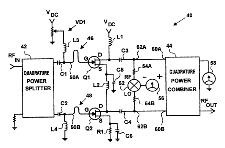
Referring now to FIGURE 7, an rf power amplifier 40 includes parts as
5 named and described in conjunction with FIGURE 1, except that the fixed
voltage
divider FD1 has been replaced by the variable voltage divider VD1, and except
that a quadrature power splitter 42 and a quadrature power combiner 44 have
replaced the power splitter 12 and the power combiner 14 of FIGURE 1. In
addition, a larger phase-adjusting loop, or tuning loop 46, and a smaller
phase-
10 adjusting loop, or tuning loop 48, have been inserted into conductors 50A
and
50B, respectively. Also, an rf mixer 52, resistors 54A and 54B, a voltmeter
56, and
a power meter 58 have been added.
Operation of the rf power amplifier 40 is the same as that of the rf power
amplifier 10 of FIGURE 1, except for two general areas of improvement. First,
15 some of the added components, as listed above, provide means for measuring
a
voltage that is a function of any out-of-phase condition that may exist at rf
inputs
60A and 60B of the quadrature power combiner 44. Other of the added
components provide means for correcting any imbalance in the amplitude of rf
signals supplied to the quadrature power combiner 44.
Obviously, frequencies provided by the quadrature power splitter 42 will be
equal, and frequencies in conductors 62A and 62B will be equal, so that equal
frequencies will be applied to the RF and LO inputs of the rf mixer 52.
Therefore,
any phase error in the quadrature inputs to the rf mixer 52 will show up as a
do
voltage at the voltmeter 56. While a given do voltage will not represent a
known
phase error, the fact that there is a do voltage will indicate that a phase
error exists.
Further, the polarity of the do voltage will indicate the direction of the
phase error.
Referring now to FIGURES 7, 10A, and 108, a jumper 64 of FIGURE 10B is
attached to the larger phase-adjusting loop 46 and is used to shorten the loop
46
to whatever length 66 provides the least do voltage on the voltmeter 56.
Obviously, an increasing voltage indicates changing the length 66 of the loop
46
in the wrong direction. After removing an excess portion 68 of the loop 46,
the
voltmeter 56 may indicate a need to reposition the jumper 64 somewhat.
CA 02432778 2003-06-19
16
Continuing to refer to FIGURE 7, subsequent to correction of phase angles,
equalization of the magnitude of the rf signals is achieved by adjusting the
voltage
that is supplied by the variable voltage divider VD1, thereby reproportioning
the
voltages that are applied to the gates of the FETs Q1 and Q2, and thereby
selectably proportioning the voltages across the FETs Q1 and Q2, as described
previously.
Referring now to FIGURE 8, an rf power amplifier 70 includes all of the
parts shown and described in conjunction with FIGURE 7, the difference being
that
the phase-adjusting loops, or tuning loops, 46 and 48, have been relocated.
Since
the mixer 52 is located immediately ahead of the quadrature power combiner 44,
phase correction can be made either before or after amplification by the FETs
Q1
and Q2. Therefore, the embodiments of FIGURES 7 and 8 provide equal
advantages, except that any phase-angle errors introduced by the FETs Q1 and
Q2
will not be detected by the embodirnent shown in FIGURE 7.
Referring now to FIGURE 9, an rf power amplifier 80 includes all of the
parts shown and described in conjunction with FIGURES 7 and 8. In addition the
rf amplifier 80 includes high-power rf amplifiers 82A and 82B and coupling
capacitors C7 and C8 that are interposed between respective ones of drain
terminals of the FETs Q1 and Q2 and the quadrature power combiner 44.
Thus, the mixer 52 is located to provide voltages that are indicative of
phase angle errors that occur after high-power amplification, and adjustment
of the
larger tuning loop 46 is effective for correcting phase-angle errors that
occur up to,
and in, the high-power amplifiers 82A and 82B. While the tuning loops 46 and
48
have been shown located as in FIGURE 8, obviously, the tuning loops 46 and 48
can be located as shown in FIGURE 7. That is, the tuning loops 46 and 48 must
be located ahead of the quadrature power combiner 44.
While the preceding discussion has focused on use of GaAsFETs in totem
pole circuit at microwave frequencies for frequencies of 3 Ghz, or higher,
there are
also efficiency advantages to using the totem pole circuit at lower
frequencies,
such as the "L" and "S" bands (1 to 3 Ghz).
At these lower frequencies, silicon bipolar transistors operated in Class C
are the most commonly used amplification device. However, GaAsFETs, in totem-
CA 02432778 2003-06-19
17
pole arrangement, provide an improvement in amplifier efficiency over that
achieved by the use of silicon bipolar transistor amplifiers.
There are two basic reasons for this improvement in efficiency. First, the
GaAsFETs, with efficiencies up to seventy percent, are inherently more
efficient
than silicon bipolar transistors at "L" and "S" bands. Second, the high gain
of
GaAsFETs at "L" and "S" bands (up to 20 Db) versus silicon bipolar transistors
(about 10 Db) result in fewer total amplification stages to achieve the
desired rf
power output.
Therefore, the use of GaAsFETs at these lower frequencies results in the
elimination of stages) and allows for lower power driver stages. And the high
gain
of the GaAsFETs makes the power-added efficiency (PAE) higher than that of
traditional Class C silicon bipolar transistors despite the Class A or A/B
operation of
the GaAsFET.
While GaAsFETs have been shown and described, it should be understood
that the principles taught herein may be applied to other types of solid-state
current
devices.
With regard to methods of the present invention, a method for minimizing
power losses when combining rf signals in two conductors that are at
quadrature
phase angles includes: producing a do voltage that is a function of a phase-
angle
deviation from quadrature; and correcting the phase-angle deviation. The
producing step includes mixing the rf signals; and the correcting step
includes
nulling the do voltage. The nulling step includes tuning a length of a
selected one
of the two conductors.
The tuning step includes interposing a larger tuning loop into the selected
one of the conductors; interposing a smaller tuning loop into the other of the
conductors; and adjusting an effective length of the larger tuning loop. The
adjusting step includes sliding a slider over the larger tuning loop.
Preferably the
tuning step includes removing an excess length from the larger tuning loop
subsequent to the sliding step. Optionally, the method includes readjusting
the
effective length of the larger tuning loop subsequent to the removing step.
Methods of the invention include: replacing a grounding resistor of the rf
combiner with a power meter; using the power meter to measure a power loss
that
is a function of an inequality in amplitudes of the rf signals; and equalizing
the
CA 02432778 2003-06-19
18
amplitudes of the rf signals as indicated by reductions in the measured power
loss.
Optionally, methods of the invention include: measuring a power loss that is a
function of both a phase-angle deviation and an inequality in amplitudes of
the rf
signals; and equalizing the amplitudes of the rf signals as indicated by
reductions
in the measured power loss either prior to or subsequent to the step of
correcting
the phase-angle deviation.
Methods of the present invention includes series connecting upper and
lower solid-state current devices between a do supply voltage and a lower do
voltage; splitting an rf input signal into two quadrature rf signals;
separately
amplifying the quadrature rf signals in the upper and lower solid-state
current
devices; quadrature combining the separately-amplified quadrature rf signals;
determining a phase-angle deviation from quadrature that exists between the
separately-amplified quadrature rf signals prior to the combining step;
correcting
the phase-angle deviation prior to the combining step; and the correcting step
comprises producing a do voltage that is a function of a phase-angle deviation
from
quadrature.
Additionally, the correcting step includes, either prior to or subsequent to
the correcting of the phase-angle deviation, measuring a power loss that is a
function of an inequality in amplitudes of the separately-amplified rf
signals, and
reducing the measured power loss. The reducing step includes adjusting a bias
voltage of one of the solid-state current devices.
The present invention can be characterized as connecting a plurality of
field-effect transistors in series for do operation while the same transistors
operate
in parallel for rf operation. Additionally, the present invention provides a
method
for minimizing the rf impedance from field-effect transistor sources to a
circuit
ground, thereby maximizing dc-rf conversion efficiency while minimizing
interference between field-effect transistors, and between field-effect
transistors and
power supply, by design and selection of decoupling capacitors and rf chokes.
Finally, in addition to characterization of the present invention as provided
in the preceding paragraph, the present invention can be characterized as
having
means for correcting phase errors in quadrature rf signals, and as having
means for
correcting amplitude inequalities in quadrature rf signals prior to quadrature
combining.
CA 02432778 2003-06-19
19
While specific apparatus and method have been disclosed in the preceding
description, it should be understood that these specifics have been given for
the
purpose of disclosing the principles of the present invention, and that many
variations thereof will become apparent to those who are versed in the art.
Therefore, the scope of the present invention is to be determined by claims
included herein without any limitation by numbers that may be parenthetically
inserted in the claims.
Industrial Applicability
The present application is applicable to rf power amplifiers in which
quadrature signals are mixed, and there is a need or a desire to minimum power
losses that are caused by deviations in phase angles from quadrature andlor
differences in signal amplitudes.