Note: Descriptions are shown in the official language in which they were submitted.
CA 02432888 2003-06-20
WO 02/065634 PCT/US02/01025
POWER AMPLIFIER SYSTEM HAVIhTG FiZEQUENCY AND AMPLIFIER FAILURE
COMPENSATION
The present invention is directed to an RF power amplifier system for use in
amplifying
an RF input signal and is more particularly directed toward frequency and
amplifier failure
compensation.
RF power amplifier systems axe known in the art for use in amplifying RF
signals for
broadcasting purposes, including radio and television. ~ ' Such power
amplifiers may be
employed in the broadcasting of either analog television signals, known as the
NTSC, PAL,
SECAM format, or digital signals, sometimes known as DTV format. When employed
in
~.o television broadcasting, the frequency bandwidth for the television
signals is 6 MHz. The
television channels will be in the UHF signal xange from appxoximately 470 to
860 MHz.
The RF input signal to such a power amplif~.er is obtained from an.IZF exciter
and, for
example, this may take the form of a modulated 1ZF carrier within a frequency
band of 470 to
860 MHz with the bandwidth of any one channel being on the order of 6 MHz.
This RF input
signal may have a magnitude omthe order of 20 milliwatts. This input signal is
increased in
magnitude to a much higher level such as on the order of 400 watts which
represents a gain on
the order of 43 d8.
These power amplifier systems are expected in many situations to be constantly
operating so that a radio or television station employing such a power
amplifier system may
2o continuously broadcast.
Broad band RF power amplifiers are often required to have a flat gain over the
specified
frequency range. Usually, an automatic gain control (AGC) closed-loop system
is used to
control the gain of an amplifier. Most AGC closed-loop controllers are analog,
however, the
AGC can be digital by using a microprocessor for complex algorithms. A
potential integxal
differential (PID) algorithm based AGC closed-loop controller can be used to
control the gain
of a power amplifier. A PID controller for AGC, which includes both analog and
digital
components, can automatically adjust the gain, compensating for fine
variations caused by the
temperature changes or a power supply voltage change. It has been widely used
in industrial
control.
3o The regular closed-loop AGC control system of a RF power amplifier
operating at
nominal frequency can be described in the block diagram of Fig.10 and Equation
A.
Pout( jc~) _ G. ~ G~(jm) ~ GP( jrv), Equation A
PZn(jcv) 1+G4~G~(jc~)~GP(jr~)
1
CA 02432888 2003-06-20
WO 02/065634 PCT/US02/01025
The ideal RF sensor characteristics are:
V;n = GI*P;n Expression (1)
Vont = Go'~Pout . Expression (2) '
Here,
c~: Frequency (w = 2~cf )
Pin (j c~) : Input dower signal at nominal frequency
Pout(j~): Output power signal from amplifier 602 at nominal
frequency
Vin: Voltage signal from input power sensor 600 at nominal
1o frequency
Vout~ Voltage signal from output power sensor 620 at nominal
frequency
G==GI (j~) :Transfer Function of input power sensor at, nominal
frequency
Go=Go(jcoN) :Transfer Function of output power sensor at nominal
frequency
G~(jce~) : Transfer function of PID controller
GP(ja~) : Transfer function for plant (controlled object)
c~N: Nominal frequency
2o The amplifier itself can contain several sub-amplifiers, which work in
parallel. The
failure of one of them changes the overall gain. A simple AGC controller would
restore the
gain. Ievel by increasing the RF drive level. That would overdrive the working
sub-amplifiers
and sacrifice the overall performance. The degradation in performance can not
be adjusted
nor compensated by the AGC, since the amplifier is driven into non linear
working region.
A cancellation technique can be used to correct gain variatioils by correcting
the
variation of the input and output signals from the RF sensors, which are due
to the
frequency response of these sensors, before the signals are used for the PID
AGC algorithm.
A similar technique can be used to compensate the gain variation caused by sub-
amplifier
2
CA 02432888 2003-06-20
WO 02/065634 PCT/US02/01025
failure.
The present invention includes a power amplifier system for use in amplifying
ari RF
input signal comprising a signal modulator that receives and modifies said
input signal and
provides therefrom a modified input signal, given operating frequency within a
known
range of frequencies and comprising a signal modulator that receives and
modifies said
input signal and provides therefrom a modified first signal, a power
amplif~.er that receives
and amplifies said modified first signal, a first power detector that detects
said input signal
and provides therefrom an average input power signal representative of the
average input
power thereof, and a second power detector connected to the output of said
amplifier for
1o providing an output average power signal representative of the average
output power
thereof, a controller that adjusts the magnitude of said average input power
signal and the
magnitude of said average output power signal as a function of the frequency
level of said
operating frequency, and, said controller inciudes a comparator that compares
the adjusted
said input average power signal and said adjusted output average power signal
and conixols
said modulator in accordance therewith.
Advantageously, a power amplifier system is provided for use in amplifying an
RF
input signal at a given operating frequency within a known range of
frequencies. The
system includes a signal modulator that receives and modifies an RF input
signal and
provides therefrom a modified first signal. At Ieast one power amplifier is
provided that
2o receives and amplifies the modified first signal. A first power detector
detects the input
signal and provides therefrom an average input power signal representative of
the average
input power thereof. A second power defector is connected to the output of the
amplifier
and provides an output average power signal representative of the average
output power
thereof. A controller adjusts the magnitude of the average input power signal
and adjusts
fhe magnitude of the average output power signal as a function of .the
frequency Ievel of the
operatirzg frequency. The controller includes a comparator that compares the
adjusted input
average power signal with the adjusted output average power signal and
controls the
modulator in accordance therewith.
The invention will now be described, by way of example, with reference to the
3o accompanying drawings in which:
Fig.1 is a schematic-block diagram illustration of apparatus employed in one
embodiment of the invention;
Fig. 2 is a block diagram of a detector in accordance with the invention;
Fig. 3 is a schematic-block diagram of an integrator;
CA 02432888 2003-06-20
WO 02/065634 PCT/US02/01025
Fig. 4 is a flow diagram of one routine involved in the invention;
Fig. 5 is a flow diagram of another routine involved in fine invention;
Fig. 6 is a flow diagram of another routine involved in the invention;
Fig. 7 is a flow diagram of anothex routine involved in the invention;
Fig. 8 is a flow diagram of anothex routine involved in the invention;
Fig. 9 is a flow diagram of another routine involved in the invention;
Fig.10 is a block diagram of a prior art closed-loop automatic gain control
(AGC)
control system for a power amplifier;
Fig.11 is a block diagram similar to that of Fig.10, but illustrating the
manner in
~o which the closed-loop gain is affected by the frequency dependent
characteristics of
sensors 600 and 620;
Fig.12 is a block diagram based on Fig.1 herein showing frequency compensation
for the input power sensor 60 as well as for the output power sensor 62;
Fig.13 is a flow diagram of another routine involved in the invention;
z5 Fig. 24 is a flow diagram of another routine involved in the invention;
Fig.15 is a block diagram of a prior art amplifier system similar to that as
shown in
Fig.10, but additionally illustrating power reduction factor F1 caused by the
failure of one or
more sub-amplifiers;
Fig.16 is a block diagram based on the block diagram herein of Fig.1 and
illustrating
2o that the power amplifier which is comprised of a plurality of parallel sub-
power amplifiers
PA-1 to PA-M and exhibits a power reduction factox Fl; and,
Fig.17 is a block diagram similar to that of Fig. 16 but.showing both
frequency
compensation and sub-power amplifier compensation.
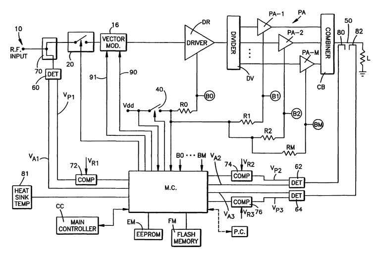
Fig.1 illustrates a power amplifier system which receives a modulated RF input
25 signal at an input terminal 10 and amplifies the, signal and supplies it to
a load L, which may
take the form of a transmitting antenna and associated equipment. The RF input
signal may
have a magnitude on the order of 20 milliwatts and have a frequency within the
UHF
frequency range between 470 and 860 MHz with a 6 MHz bandwidth for the
television
channel involved. The signal may be increased by the amplifier with a gain on
the order of
30 43 dB so that the output signal as applied to the Ioad L may be on the
order of 400 watts.
The RF input signal is applied to the input terminal 10 and, thence, to a
vector
modulator. The vector modulator changes the magnitude and the phase of the RF
signal.
The modified RF signal from the vector modulator is then amplified by a driver
DR to a
higher level, such as 20 watts. The output, as taken.from the driver DR, is
then supplied to a
CA 02432888 2003-06-20
WO 02/065634 PCT/US02/01025
power divider DV, sometimes referred to as a signal or power splifter, which
divides the
amplified signal by a factor of M. M signals are then applied to M~sub-power
amplifiers PA-
1 through PA-M, where M, for example, may be 12. The signals from the sub-
power
amplifiers PA-1 through PA-M are then combined in a signal combiner CB to
provide an
output signal which is applied to the load L.
The input signal is applied to a vector modulator 16 when the RF input switch
20 is
closed. The RF switch 20 is controlled by a microcontroller MC, as will be
explained in
greater detail hereinafter. The microcontroller also controls the vector
modulator to vary the
phase and gain of the RF signal.
1o The driver DR amplifies the signal with a gain of approximately Z4 dB to
deliver an
RF signal of approximately 20 watts to a divider. DV. This divider serves as a
power sputter
and splits the applied RF signal into N,portions. The divider applies N equal
portions of the
RF signal to respective sub-power amplifiers PA-1 through PA-M. Each sub-power
amplifier inay include a field effect transistor having its drain electrode
connected through a
suitable resistor, such as resistor R1 or R2 or RM, to a DC switch 40. When
this switch is
closed, it connects each drain electrode with a DC voltage source VbD. This
voltage source
may, for example, be on the order of 32 volts.
The outputs from the power amplifiers PA-1 through PA-M are combined at the
power combiner CB. The output signal at the output circuit 50 is on the order
of 400 watts.
2o The microcontroller MC monitors the operation of the amplifier system and
controls
the system by varying the phase and or gain of the RF signal and controlling
the operation of
the RF switch 20 and the DC switch 40.
When the DC switch 40 is closed, current will flow in the power amplifiers PA-
2
through PA-M. This current will flow through the associated resistors R1
through Rm. A
voltage is developed across each resistor. These voltages are supplied as
current samples to
the microprocessor MC which then determines whether fhe current levels are too
high or too
low and takes appropriate action. Also, when the switch 40 is closed current
flows through
resistor RO and the driver DR. The voltage developed across this resistor is
also supplied to
the microcontroller MC for analysis.
so In addition to moxutoring the current flowing through the various power
amplifiers,
the microcontroller also monitors peak and average power levels with the use
of power
detectors. These detectors include an input power detector 60 and output power
detectors
62 and 64. The power detector 60 is connected to an input signal divider 70
and serves to
provide DC output signals V~ and VAl respectively representative of the input
peak power
CA 02432888 2003-06-20
WO 02/065634 PCT/US02/01025
and the input average powex. The signal representative of the input peak power
V~ is
compared with a reference V~ at comparator 72. Tf the peak power V~ exceeds
the reference
then an interrupt signal is supplied to the microprocessor MC which interrupts
the routine
being processed and enters a fault process to turn the power amplifier system
off.
Detector 62 is connected to a incident signal coupler 80 coupled to the output
transmission line 50. This detector 62 provides a DC voltage signal VP2
representative of the
peak output power as well as a DC voltage V,~ which represents the average
output power
in the forward direction at the output transmission line 50. Signal VPZ is
compared with a
reference V~ at comparator 74. Tf signal V~ exceeds reference V~ fhen an
interrupt signal is
1o supplied to microcontroller MC which then enters a fault process routine to
turn the power
amplifier off.
A coupler 82 is employed for sensing the reflected power and this coupler is
connected to detector 64. This detector 64 serves to provide DC voltage
signals including a
signal VP3 representative of the peak reflected power and VA3 representative
of the average
reflected power. If signal VP3 exceeds a reference V~, then comparator 76
applies an
interrupt signal to the microcontroller MC which then enters a fault process
routine to turn
the power amplifier off. The monitored average power signals VA1, V,~ and VA3
are supplied
to the microcontroller MC which is programmed to vary the gain and/ or phase
of the RF
signal as needed.
2o Each of the power detectors is constructed in the same fashion as detector
60 is
described with reference to Fig. 2. This detector includes an envelope
demodulator 61 which
receives a sample of an RF signal from correspondingly input or output
transmission lines.
The carxier signal may, for example, be on the order of 600 MHz and the
baseband for fhe
television signal has a bandwidth of ~6 MHz. The demodulator 61 effectively
strips off the
carrier signal (600 MHz) leaving only the demodulated baseband signal. This
signal may be
viewed as an analog positive signal and which is applied to the integrator 63
and a peak
power detector 65.
The integrator 63 provides an output signal in the form of voltage VAl
representative
of the average input power whereas the peak detector 65 provides an output
signal in the
3o form of a voltage V~ representative of the peak input power. The
demodulator 62 and the
integrator 63 form an RMS detector.
The integrator 63 located in each of the detectors 60, 62 and 64 may take the
form as
illustrated in Fig. 3 to be described below.
As will be recalled, the digital 8-VSB format refers to an 8 Ievel vestigial
sideband
CA 02432888 2003-06-20
WO 02/065634 PCT/US02/01025
signal. The baseband of this signal is 6 MHz wide. It is desired to provide
efficient power
level control of the power amplifier system illustrated in Fig. 1. To achieve
this, it is desirous
to provide a power detector that provides an output signal, Vo"t, which is
proportional to the
corresponding average power. In the past, circuit designers have typically
employed true
RMS detectors for converting an input baseband signal into a DC Ievel
proportional to the
RMS power. This is done in accordance with the equation noted below.
T
~'V.,~ dt
V~ T
A significant problem in a power amplifier system as shown in Fig.1 is the
complexity
and expense of the circuitry to perform the above equation. At present,
commercially available
2o integrated circuits that perform this type of an equation are only suitable
for use at low
frequencies, such as up to 10 kHz. As such, they are not able to provide an
RMS signal
representative of a baseband signal that is of a substantially higher
frequency, such as being 6
MHz wide as in the case of digital television signals. There is a need to
provide a circuit that
will deliver an output voltage Vout which is proportional to the RMS value of
the input voltage
s5 V;~ without employing multiplication (such as V;~ times V;~ to obtain.
V~,Z). This is achieved with
the circuit shown in Fig. 3 as described below.
The input voltage V;~ is applied to an input terminal 100 and the output
voltage Vo"t is
obtained at an output termina1102. A wideband operational amplifier 104 is
provided having
an RC charge path connected to its positive or non-inverting input '106 and an
RC discharge
2o path is connected to its inverting or negative input 108. The charge path
includes a resistor R2
and a capacitor C1 having their junction point connected to input 106 of
amplifier 104. The
other side of capacitor C1 is connected to circuit ground. The discharge path
includes a resistor
R2 and a capacitor C2 having their junction point connected to input 108 of
the operational
amplifier 104. The other side of capacitor C2 is connected to circuit ground.
A diode D1 is
25 connected between the output 105 of amplifier 104 and the circuit output
202. The circuit
output 102 is connected to the negative input 108 of the amplifier 104 by way
of a circuit
path 110.
The circuit in Fig. 3 has separate RC circuits that define the charge and
discharge time
constants acid thereby provides independently controlled charge and discharge
times. The
CA 02432888 2003-06-20
WO 02/065634 PCT/US02/01025
circuit may be tuned by changing the value of resistors R1 and R2 so that the
ratio of the charge
and discharge time constants allows the detector to deliver an output voltage
Vout proportional
to the RMS value of V;~. The manner of operation involved is presented below.
Consider a situation wherein the diode D1 is connected between output 105 and
circuit
output 102 and that R2*C2 > R1*C1.
In this situation, the voltages Vo"t and V- will follow voltage V+ as voltage
V+ increases.
The moment voltage V+ decreases, voltage Vout follows the discharge time R2*C2
until V+
increases again and the operation repeats. Since voltage V+ follows voltage
V;~ with a charge
time constant R1*C1, then voltage Vout follows voltage V;~ with the C1*R1 time
constant on the
1o rise and the C2*R2 time constant on the voltage V;~ fall.
When the R2*C2 time constant is long enough ( c~ ~ ~ < f~oW
where flow is the lowest frequency in the spectrum of the envelope demodulated
signal) this
allows creation of the voltage Vo"t anywhere in the range from voltage V;~
max. to voltage V;
avexage by manipulating the C1*R1 time constant from C1*R1=0 to C1*R1=C2*R2.
2s If the diode D1 is replaced by diode DZ (as shown by the broken line) the
condition
R1*C1 > R2*C2 results. If R1*C1 is Iong enough ( * < flow ) then this allows
creation
CI Rl
of voltage Vout anywhere in the range from V;~ average to V;~ m;n;mmn, varying
C2*R2 from =
C1*R1 to zero.
In the power amplifier system of Fig.1, it is contemplated that an 8-VSB
baseband signal
2o is involved. It's spectrum looks like white noise with a frequency range
from 0 to 6 MHz and
almost even distribution of power within the range. The goal is to tune the
ratio of charge and
discharge time constants for the detector to deliver voltage Vout proportional
to the RMS value
of voltage V;~ without going through a multiplication (V;~*V;~), which would
require circuit
complication.
25 This is achievedby referencingvoltage Vout originatedby 8-VSB modulated RF
to voltage
Vo"t originated by CW. Since the modulation baseband of the nonmodulated
(CW)RF signal is
equal to zero, voltage V;~ is a I7C voltage. .The RMS value for the DC voltage
is equal to the
voltage itself. Applied as voltage V;~, it will appear as Vout=V;~'on the
output of the deteetor.
CA 02432888 2003-06-20
WO 02/065634 PCT/US02/01025
The level of this voltage Vout can be used as a xeference of RMS voltage for a
given average
power of RF and, after switching from CW to 8-VSB signal with the same average
power level,
tune the time constants so that the voltage Vout shows the same value.
The way to tune the time constants is to adjust fhe values of resistors R1 and
R2 to
achieve a certain voltage Vout. Thus, the RMS detector delivers true RMS value
for two kinds
of RF modulations: CW (no modulation) and 8-VSB.
Fig. 3 discloses a non-modulated continuous wave (CW) signal of a known power
level
Pr may be applied to the RF input terminal 10 (see Fig.1). The value of
voltage Vout is observed.
" The continuous wave may then be replaced with an 8-VSB source of the same
known power
level Pr. Again, the output voltage Vo"t is observed. Since the input power
levels were the same
Pr, the value of voltage Vout should be the same for both cases. If it is not
the same, then the
values of resistor R1 and R2 in the charge and discharge paths, are varied to
change the ratio
of the charge and discharge time constants. Once the output voltages are the
same then the
values of the resistors are fixed and thus they have been optimized to achieve
the same voltage
Vout for both CW and 8-VSB baseband signals.
Reference is now made to the flow diagrams of Fig. 4 through Fig. 9 which
illustrate the
manner in which the microcontroller MC is programmed to accomplish various
functions
herein.
Attention is specifically directed to Fig. 4 which illustrates the flow
diagram for the fault
2o process routine 200 which is employed for turning off the power amplifier
when a fault
condition has been determined. In step 202, a "module off" indication has been
made because
a condition (to be discussed in greater detail hereinafter) has been
determined to be a fault and
the module (i.e. the power amplifier of Fig.1) is to be turned off. This may
be accomplished by
the microcontroller MC controlling the RF switch 20 and the DC switch 40 by
opening the
switches and by adjusting the modulator 16 for minimum gain,
The procedure then steps to a three-strike process 204 during which the power
amplifier
is turned on and the conditions are again monitored to determine if there is a
fault condition.
In this case, the power amplifier is turned on up to three times over a 10
second interval to
determine whether the fault condition is still present.
so~ Thereafter, the procedure advances to step 206 which determines whether
the power
amplifier has been successfully turned on during the three-strike process. If
it has been
successful, then the procedure advances to step 209 and continues monitoring.
If the attempt
to restart the power amplifier is not successful, then the procedure advances
to step 208 during
which.the power amplifier is shut down and not restarted. This shut down
procedure involves
CA 02432888 2003-06-20
WO 02/065634 PCT/US02/01025
the microcontroller commanding the RF switch 20 to open and comma"ding ~,e DC
switch 40
to open as well as turning down the gain of the vector modulator 16.
Fig. 5 illustrates an emergency process routine 250 which is employed by the
micxocontroller in fhe event that emergency Ievel faults have been detected.
This routine
includes step 252 during which the microcontroller responds to an interrupt
signal received
from one of the peak power compaxators 72, 74 or 76 to interrupt the
micxocontroller and enter
into fhe fault process routine 200, described above wifh reference to Fig. 4,
for purposes of
turning off the power amplifier module of Fig. 1. Comparator 72 provides such
an interrupt
signal when the input peak power signal V~ is greater than a reference signal
VRl. Similarly,
2o comparator 74 provides such an interrupt signal when the output forward
peak power signal
V~ exceeds a reference V~. Also comparator 76 provides such an interrupt
signal when the
reflected peak power signal VP3 exceeds a reference VR3 (representative of a
VSWR excessive
condition).
Fig. 6 illustrates a fast monitor process routine 300. In this routine, a
determination is
made at step 302 as to whether any of the pallets or sub-power amplifiers PA-1
through PA-M
have an overloaded current condition. If so, then fhe procedure advances to
the fault
process 200 (see Fig. 4). If not, the procedure advances to step 304.
Before proceeding with step 304 attention is now directed to Fig. 7 which
illustrates a
routine for determ~nrng whether one of the sub-power amplifiers PA-1 through
PA-M has an
over-current condition. This routine commences with a start step 303 and, in
the monitoring
operation, a current sample TSl representative of the current flowing in the
sub-power amplifier
PA-1 is obtained in step 305. In step 307, the current sample IS1 is compared
with a reference
sample IH representative of a high level of acceptance. If the current sample
exceeds this high
level, the procedure advances to the fault process 200 discussed hereinbefore
with reference to
Fig. 4. This type of routine may be practiced for monitoring each of the sub-
power amplifiers
PA-1 through PA-M.
Attention is again directed to routine 300 in Fig. 6. If none of the power
amplifiers are
current overloaded, as determined in step 302, the procedure advances to step
304 wherein a
determination is made as to whether the input power is overloaded. In this
step, a signal
so representative of the average input power is signal VA1 and this is
compared with a reference
of an acceptable level in the microcontroller MC. If an overload condition is
determined, the
procedure advances to the fault process 200.
If the input power is not overloaded, the procedure advances to step 308 at
which a
determination is made as to whether the output power is overloaded. This is
accomplished by
~o
CA 02432888 2003-06-20
WO 02/065634 PCT/US02/01025
comparing the signal V~, representative of the averag ouput power, with an
acceptable
reference level. Of signal V~ exceeds the reference Ievel, the procedure
advances to the fault
process routine 200. If not, then the procedure to step 310. ,
In step 310 a determination is made as to whether the reflected power is
overloaded.
This is determined by comparing the average reflected power signal VA3 with a
reference Ievel
and if the reflected power is overloaded, the procedure advances to the fault
process
routine 200. Reference is now made to Fig. 8 which illustrates a slow monitor
process
routine 350. In this routine, a determination is made at step 352 as to
whether the DC voltage
(V~D) is too high. This is accomplished by comparing the voltage with a
reference level. If the
so voltage VDD is too high, the procedure advances to the fault process 200.
If not, the procedure
advances to step 354.
In step 354, a determination is made as to whether the heat sink temperature
is too high.
This is obtained by comparing a signal representative of the heat sink
temperature from a
suitable source 81 with a reference. If the heat sink is overloaded, the
procedure advances to
the fault process routine 200. Otherwise, the procedure advances to step 356.
In step 356, a determination is made as to whether there has been an automatic
gain
control failure (AGC failure). If so, the procedure advances to the fault
process routine 200.
Otherwise, the monitoring operation continues.
Fig. 9 illustrates the automatic gain control (AGC) routine 400. This
procedure includes
2o step 401 during which the average sub-PA current I ave. is determined for
each sub-PA; that is
determine the value of Ii for from i = 0 to i = M and then divide the sum by
M, the total number
of Sub-PA. The procedure then advances to step 403.
In step 403, a determination is made as to how many of the sub-PA (PA-1
through
PA-M) failed. This is done by determining if the current Ii at each sub power
amplifier is equal
z5. to or less than Io, where Io is a threshold for "zero" current and is set
to a value on the order of
10% to 20% of I ave. Step 403 then sets K to the number of failed sub-Pas. The
procedure then
advances to step 405. .
In step 405, a determination is made as to whether K exceeds X, where X is the
maximum
allowed number of failed sub-Pas. If "yes", the procedure advances to the
fault process step 200.
3o If the determination at step 405 is "no", the procedure advances to step
407.
In step 407, the value of the output power signal P°ut(N) is re-
calculated by multiplying
the measured value of the output power signal by the ratio of M K . The
procedure then
11
CA 02432888 2003-06-20
WO 02/065634 PCT/US02/01025
advances to step 408.
In step 408, the confrol output signal variation ~ V is generated as presented
in
the block bearing the label 408.
The procedure then advances to step 410 at which a determination is made as to
s whether the absolute value of D V is greater than d ~ (i.e. is ~ ~ V~ > d ~
) . If so, the
absolute value of 0 V (i.e. ~ ~ V~ ) is made equal to the value of ~ ~ in step
412.
The procedure then advances to step 414 wherein the magnitude of the control
voltage vector VM is updated so that it is equal to VM + ~ V.
The procedure then advances to step 416 wherein a check is made that the
control
so voltage vector VM is greater than 0 but is less than the full scale value
of VM which is
used herein as Vng..
The procedure then advances to step 418 wherein the microcomputer reads the
phase signals which are referred to as c~ and c~ from the external source 83
(Fig.1).
2
These signals are used in the following. The procedure advances to sfep 420
wherein
Zs a determination is made that ~ is greater than 0 but Less than ~ (i.e. 0<~<
The procedure then advances to step 422 wherein the vectors to be supplied to
the vector modulator 26 are generated. This includes the I~e~tor which is
equal to VM cosc~
and the Qve~tor which is equal to VM sine .
2o The procedure now advances to step. 424 wherein the Lector ~d ~~e Qv~tor
are
supplied to the vector modulator 16 to vary the phase and gain of the signal
being
processed by the vector modulator 16.
Thereafter, the procedure advances to step 426 during which a suitable time,
such
as 20 milliseconds, is waited. Then, the procedure advances to step 428 during
which
2s a determination is made as to whether or not the AGC control has failed. If
so, the
procedure advances to the fault process procedure 200 (see Fig. 4).
To maintain the gain of the power amplifier constant at different operational
frequencies, the cancellation technique employs compensation factors to
correct the
2z
CA 02432888 2003-06-20
WO 02/065634 PCT/US02/01025
input and output power, then the PID AGC algorithm will use corrected data to
generate control signals.
The closed-loop AGC control system, without using the cancellation technique
for input and output power sensors can be described by the block diagram
Fig.11 and
s Equation B. Thus, the system closed-Ioop gain will be affected by the
frequency
characteristics of the sensors.
Pout( jc~) _ G~ . Ga( jw) . G~( j~) . GP( j~) Equation B
Prrz(jw) ~l+Go~Gaur(jw)~G~(jw).Gp(j~)~
The real IZF sensor characteristics are:
V~(jc~) - Gin (jcc~) *GI*Pin - Expression (3)
1~ Vout ~.7~~ - Gout (~~)'~Go'kpout E~preSSlOn (4)
Here,
Pin(jw) : Input power signal as a function of frequency
Pout(j~)~ Output power signal as a function of frequency
G==GI(jc~N) :Transfer, Function of input power sensor at nominal
s5 frequency
Go=Go(j~N):Transfer Function of output power sensor at nominal
frequency
Gin(jc~) : Gain factor of input power sensor due to frequency-
dependency
20 Gout (j~) : Gain factor of output power sensor. due to frequency-
dependency
GI*Gin (jc~) : Transfer Function of input power sensor ,with
frequency-dependence
I3
CA 02432888 2003-06-20
WO 02/065634 PCT/US02/01025
Go*Gout (jc~) :Transfer Function of output power sensor with
frequency-dependence
Vin (jcv): Voltage signal from input power sensor with
frequency-dependence
Vout (.7 ~~ : Voltage signal from output power sensor with frequency-
dependence
Since Equations A and B are different closed-Loop transfer functions, a
regular
PID algorithm based AGC controller can not generate the same gain for the RF
amplifier if it is operated at any frequency other than nominal frequency.
The closed-loop AGC control system using the cancellation technique for
Zo input and output power sensors can be described in the block diagram of
Fig.12 and
Equation C.
Pour(j~) _ G..Ga(jw).Fr~(jw).G~(jw).GP(jev) EquationC
Pa(jCV) ~l+Go~Gour(jw)~Faur(j~)~Gc(jw).GP(jw)~
After compensation, the signals will be:
- Fin (~~) *~in (J~~ - Fin (~~) *Gin (]~) *G=*Pin
Expression (5)
V ~ out ( ~ ~ ) - ~' out ( J ~ ) * Vout (J ~ ~ - Fout ( ~ ~ ) * Gout ( ~ ~ ) *
Gp * Pout
Expression (6)
Here,
Gin(j~a) : Gain factor of input power sensor due to frequency-
2o dependency
Gout (jc~) : Gain factor of output power sensor due to frequency-
dependency
G==GI (jc~N) : Transfer Function of input power sensor at nominal
I4V
CA 02432888 2003-06-20
WO 02/065634 PCT/US02/01025
frequency
Go=Go (jc~N) : Transfer Function of. output power sensor .at nominal
frequency .
Fin (j~): Compensation factor function for input power sensor
Fout (7m) = Compensation factor function for output power
pin=Pin (j~N) = Input power signal at nominal frequency
Pout=Pout(j~N) : Output power signal at nominal frequency '
Vin=Vin(j~N) ~ Voltage signal from input power sensor at
nominal frequency
1o V' in (jt~) : Corrected voltage signal from input power sensor
Vout=Vout(j~N) = Voltage signal from output power sensor at
nominal frequency
V~out (j~) : Corrected voltage signal from output power sensor
t~N : Nominal frequency ,
I f , ,
Fin (J~) *Gin (j~) - ~- Expression ('7)
Fout (j~) *Gout (j~) - 1 . Expression' (8)
Then,
Vein (]~) - Fin (]~) *~in ~.7~~ - Fin (]~) *Gin (]~) *G=*Pin = G=*Pin
Vin
Expression (9)'
V ~ out ( ] ~ ) - Fout ( ] ~ ) * vout ~.7 ~ ~ - Fout ( ] ~ ) * Gout ( ] ~ ) *
Go * Pout = Go * Pout
Expression (10)
Expressions 9 and~l0 mean that any variations in the RF sensors' output due to
frequency dependency will be canceled by a compensation factor function. After
cancellation, the RF sensors seem working at norivnal frequency all the time.
Thus the
RF sensors will be frequency-independent within the specified frequency range,
this
CA 02432888 2003-06-20
WO 02/065634 PCT/US02/01025
means the PID AGC algorithm and the P,F power sensors can be used in a broad
bandwidth.
From Expressions 7 and 8, the following conclusions can be drawn:
F;~(jt~) - 1/ Gin (jco) ~ Expression (11)
Foist (jc~) - 1/ Gout (jw) Expression (12)
The inverse of the firansfer function of the RF sensors is the compensation
factors
for the cancellation of the variation of input and output power caused by the
sensors.
Thus, after cancellation Equation C can be rearranged as follows:
Pou~(jw) _ Gr.G~(jcv).GP(j~)
Pa(jcc~) 1+Go~G~(j~).GP(ja~) ~ EquationC~
This equation Equation C ~ is identical to equation A. This means the
compensated system operating at any given frequency will have the same closed-
loop transfer function as a system operating at nominal frequency and these
two
systems will have the same gain under Automatic Gain Control.
In practice, the RF power amplifier will operate at a fixed frequency ~o or f
o
once the operational frequency is set. Thus Expressions 7 and ~ can be
modified as:
F;~(jwo) - 1/Gin (7~0) Expression (13)
Foist (7~0) - 1/Gout (j~o) Expression (14)
The characteristics of frequency response of RF sensors, G;~ (jw ) and Gout
zo ( j ~ ) , can be obtained through measurement. Since the frequency response
of the
RF sensors can not be described by simple closed-form formula they are
presented in
the format of data look-up table. Also, since the look-up table has non-
continued
discrete data points, an interpolation algorithm will be ixsed to generate the
correct
16
CA 02432888 2003-06-20
WO 02/065634 PCT/US02/01025
factor at the exact frequency, even it may not be obtained directly from look-
up
table. Once the look-up tables of response vs frequency are obtained, for any
given
frequency, the variation caused by the frequency dependency of the RF sensor
can be
compensated using this technique. Since the look-up tables are stored in non-
volatile
s memory, they can be used to correct the frequency-dependent input power and
output power sensors for any given operating frequency as long as the
frequency is
within the bandwidth.
To use the cancellation technique to compensate the frequency dependence of
RF sensors, the operating frequency has to be set. -The controller can use the
1o cancellation technique to compensate the variation caused by the frequency
via look-
up table or equation. The operating frequency of the RF amplifier will be. set
via data
communication from a PC or main controller to the micro-controller MC, in
which a
digital PID algorithm based AGC controller resides.
Once the operating frequency f0 or ~o is set or updated, the micro-controller
is calculates the frequency compensation factor F;~ (jc~o ) and ' gout ( j wo
) . The
setting frequency fo or coo is stored in non-volatile memory EEPROM. Every
time
the micro-controller restarts, the compensation factors F~ (jcuo ) and Fout (
7 ~o )
will be calculated at initialization time. During normal operation, the micro-
controller uses the factors to compensate the input and output power for the
2o iteration of the PID algorithm. .
The microcontroller MC (Fig. 2) is also connected to a central or main
controller CC by way of a serial bus that may take the form of a controller
area
network (CAN) serial bus. Additionally, the microcontroller MC is connected by
a
serial communications network with a personal computer PC. The microcontroller
is
2s provided with memories including a EEPROM memory EM and a flash memory FM.
These memories may be located externally of the microcontroller or internally
thereof. The memory EM stores configuration information including the
operational
frequency fo for the power amplifier PA. 'The changes to be made in the
magnitude
of the frequency may be supplied from either the main controller CC or from
the
so personal computer PC to the controller MC which then stores the new
operating .
17
CA 02432888 2003-06-20
WO 02/065634 PCT/US02/01025
frequency f0 in memory EM. The flash memory FM stores software codes as well
as
the look-up table LUT.
The look-up table LUT stores the frequency compensation correction factors
employed for correcting the measured values of the input power signal Pa,~ and
output power Poi, as measured by the detectors 60 and 62. These correction
factors
are employed in Equation C herein. An example of the look-up table is
presented in
Table 1 below.
Table 2 (Look-up table LUT)
f G F G 'F
10(f=UJ in ~ in ~ out ~ out t
~ ~ ~ ~ ~ J ~ J w
) ) ) )
2~)
MHz
4 0 1 0 1
1570 .9925 .0075 .9193 .0878
4 0 1 0 1
80 .9883 .0118 .9323 .0726
4 0 1 0 1
90 .9899 .0102 .9452 .0580
205 0 1 0 . 1
00 .9943 .0057 .9469 .0560
5 1 0 0 1
.0005 .9995 .9577 .0442
5 1 0 0 1
2520 .0092 .9909 .9720 .0288
5 1 0 0 1
30 .0166 .9837 .9824 .0179
5 1 0 0 1
40 .0168 .9835 .9937 .0063
305 ~ 1 ~ 0 1 1
50 .0101 .9900 .0000 .0000
5 ' 1 1 0 1
60 .0000 .0000 .9988 .0012
1s
CA 02432888 2003-06-20
WO 02/065634 PCT/US02/01025
0 1 0 1
70 .9889 .1122 .9950 .0050
5 0 1 0 1
80 .9797 .0207 .9985 .0015
5 5 0 1 1 0
90 .9740 .0267 ,0073 .9928
6 0 1 1 0
00 .9691 .0319 .0150 .9852
6 0 1 1 0
2010 .9675 .0334 .0219 .9786
6 0 1 l 0
20 .9664 .0348 .0219 .9786
6 0 Z 1 0
30 .9704 .0305 .0133 .9869
~
256 0 Z 1 0
40 .9776 .0229 .0030 .9970
6 0 1 0 1
50 .9872 .0130 .9990 .0010
6 1 0 0 1
20.60 .0170 .9833 .9410 .0627
6 1 0 0 1
70 .0220 .9785 .9480 .0548
6 1 0 0 1
80 ~ .0220 .9785 .9620 .0395
256 1 0 0 1
90 .0170 .9833 .9720 .0288
7 1 0 0 1
00 .0090 .9911 .9840 .0163
7 1 0 0 1
3010 .0030 .9970 .9970 .0030
7 0 1 1 0
20 .9990 .0010 .0100 .9900
7 0 1 1 0
30 .9970 .0030 .0230 .9775
29
CA 02432888 2003-06-20
WO 02/065634 PCT/US02/01025
7 0 1 1 0
40 .9950 .0050 .0340 .9671
7 0 1 1' 0
50 .9960 .0040 .0460 .9560
7 0 1 1 0
60 .9990 .0010 .0580 .9452
7 1 0 1 0
70 .0010 .9990 .0640 .9398
7 1 0 1 0
1080 .0020 .9980 .0760 .9294
7 0 1 1 0
90 .9950 .0050 .0820 .9242
8 0 1 1 0
00 .9790 .0215 .0800 .9259
158 0 1 1 0
.9680 .0331 .0780 .9276
It is noted that the look-up table LUT in Table 1 provides correction factors
for
frequencies in the frequency range from 470 MHz to 810 MHz. Additionally, the
frequencies shown are increased in value by 10 MHz at each step. It is to be
appreciated
2o that such a look-up table may include several more frequencies. With the
frequency
correction factors for the frequencies shown, it will be appreciated that for
any
frequency located between those shown in the Table, the value of the
correction factors
may be obtained through an interpolation algorithm, common in-the art.
Reference is now made to the frequency update process routine 500 illustrated
25 in Fig.13. This process includes a step 502 during which the
rnicrocontroller determines
whether a frequency update has taken place through a serial communications
port from
either the main controller CC or from the personal computer PC. If not, the
process
loops back to make another determination. If the determinafiion in step 502 is
affirmative, then the process advances to step 504.
so In step 504, a determination is made as to whether the new frequency is
equal to
the old frequency. If so, then the procedure loops back to step 502. Tf the
determination
at step 504 is that the new frequency is not equal to the old frequency, then
the
procedure advances to step 506.
zo
CA 02432888 2003-06-20
WO 02/065634 PCT/US02/01025
In step 506, the procedure stores the new frequency fo into the non-volatile
memory {EEPROM) EM (Fig.1). Based on the frequency fo in the look-up table
LU'T and
a suitable interpolation algorithm, if needed, the correction factors are
obtained for the
input power sensor 60 and the output power sensor 62 and then the procedure
loops
s back to step 502.
Fig. 24 illustrates a power correction process routine 600. This routine
includes
step 602 wherein the input power signal P;~(N) is adjusted by multiplying the
signal
with the correction factor obtained from the look-up table (and further
adjusted by
interpolation if needed). Also, the output power signal Pout{N) is. corrected
in a similar
?o . fashion by obtaining the correction factor at the operating frequency fo.
Now that the
input and output power signals have been corrected to cancel the effects of
frequency,
the automatic gain control procedure at step 400 (Fig. 9A) is employed.
For a power amplifier with many sub-amplifiers, fhe failure of some sub-
amplifiers should not prevent the power amplifier from continuous operation
and it
Zs should not prevent the AGC controller from working. Since the PID algorithm
can not
compensate for the errors caused by the sub-amplifier failure for AGC, the
cancellation
technique is used to correct either the input or output power for the PID
algorithm. The
correction factors can be calculated from the total number of sub-amplifiers
and the
number of failed sub-amplifiers. The total power reduction factor F1 is equal
to (M-
zo K)/M. The correction factor will be M/(M-K), where M is total number of
sub-amplifiers and K is the number of the failed sub-amplifiers. The number of
failed
sub-amplifiers should be realized based on the sub-amplifiers' working
conditions.
The regular closed-loop AGC control system with failed sub-arrnplifiers can be
described by the block diagram Fig. 15 and Equation D. As we can see the
system
2s closed-loop gain will be affected by the failure of sub-amplifiers.
Pout(jw) _- GT.G~(jw).GP(j~).F~ EquationD
Pin( jw) ~1 + Ge ~ F~ . G~( jw) . GP( jw)~
By comparing Equation D with Equation A, it is seen that these two transfer
functions have different forms, thus they will not have the same gain under
same
22
CA 02432888 2003-06-20
WO 02/065634 PCT/US02/01025
PID based AGC controller.
A compensation factor is added to provide fhe block diagram of Fig.16 and
equation E:
Pour(jw) _ G~.G~(jw).GP(j~).F~ EquationE
Prn(jcv) ~1+Go~F~.G~(jcv}.Gp(jw).Fz~
Here,
Fl=(M-K}/M:Power reduction factor caused by the failure of a number
sub-amplifiers PA-1 to PA-M (Fig.1)
F2: Power compensation factor
M: Total number of sub-amplifiers
so K: Number of failed sub-amplifiers
Thus, if we let FZ =1/Fl = M/ (M-K), Equation E can be modified as:
Pout c~ . M Equation E ~
(j ) M_K _ G,.G~(jtv).Gp(jc~)
Ptn(jw) 1+Go~G~(jtr~).Gp(jc~)
By comparing Equation E" with Equation A, it is seen that the xight sides of
the two equations are identical, this means the system with failed sub-PA will
have
25 the same transfer function as that of a normal system after the
compensation. Thus
the PID algorithm could still be used for Auto Gain Conlxol. And power
amplifier
can still operate normally at reduced power without any signal distortion or
amplifier been over-driven.
Overall compensated system can be described in block diagram Fig.17 and
~~ ~"".,+;~,., ~
Pot( jw) G~ G~( jcv). F~~ jc~). G(j~). G(j~).
P~~j~} 1+C~-C~=~(jco)~Ftycv)-~ K.G(j~).~. M
M M-K
CA 02432888 2003-06-20
WO 02/065634 PCT/US02/01025
Equation F
After cancellation, we have
Pour(jw).M K G..G~(jcv).GP(jeo) EquationF~
Pca(jc~) ~ 1+Go~G~(jcv).Gp(jc~)
If there is no failed sub-amplifier, which means K=0, the equation will be
s identical to Equation A.
A power amplifier system for use in amplifying an RF input signal exhibiting
a given operating frequency within a known range of frequencies. The system
includes a signal modulator that receives and modifies the input signal and
provides
therefrom a modified first signal. A power amplifier receives and amplifies
the
Zo modified first signal. A first power detector detects the input signal and
provides
therefrom an average input power signal representative of the average input
power
thereof. A second power detector connected to the output of the amplifier
provides
an output average power signal representative of the average output power
thereof.
A controller adjusts the magnitude of said average input power signal and the
25 magnitude of said average output power signal as a function of the
frequency level
of the operating frequency. The controller includes a comparator that compares
the
adjusted said input average power signal and said adjusted output average
power
signal and controls said modulator in accordance therewith. Also, the
amplifier
includes a .plurality of sub-amplifiers that are monitored for failure and
adjustments
2o are~made to the average output power signal as needed. .
23