Note: Descriptions are shown in the official language in which they were submitted.
CA 02432936 2003-06-23
WO 02/052910 PCT/USO1/47653
MAI~IUFACTURE OF PRINTED CIRCUITS USING
SINGLE LAYER PROCESSING TECHNIQUES
BACKGROUND OF THE INVENTION
FIELD OF THE INVENTION
The present invention relates to the maalufacture of circuit boards. More
particularly, the invention relates to a continuous process for forming a
multilayered circuit structure, which prevents damage to conductive foils
during the formation of multilayered circuit structures while enhancing
etching precision and accuracy of the circuits.
DESCRIPTION OF THE RELATED ART
Circuit boaxds and printed circuits have wide application in'the field of
electronics. They ar a useful for large scale applications, such as in
industrial
control equipment, as well as in small scale devices, such as telephones,
radios
and personal computers. In producing such printed circuits, it is important
that
a high degree of accuracy and resolution is attained for very small line and
space widths to ensure good performance of the circuit.
The ability to produce accurate features having very small dimensions,
particularly of 100, or less, is extremely important in the production of
small
and large scale equipment. Etching precision becomes more important as the
circuit patterns become ever smaller. It is well lcnown in the art to use
lcnomn
photolithographic techniques to produce printed circuit boards having small
features with a high degree of accuracy. Typically, an electrically conductive
foil is deposited onto a substrate, and a photoresist is then deposited onto
the
foil. The photoresist is then imagewise exposed and developed, forming a
CA 02432936 2003-06-23
WO 02/052910 PCT/USO1/47653
pattern of small lines and spaces which are then etched into the conductive
foil.
It is a common practice to then subject the foil to a bond enhancement such as
a "black oxide" treatment, in which the copper is pre-roughened by chemical
micro-etching, and is chemically treated with a layer of copper oxide (which
is
black). This treatment helps to promote secure adhesion of the foil to otlier
materials. See, for example, the discussion in U.S. Patent No. 4,997,516,
which is incorporated herein by reference, for a discussion of forming a
blaclc
oxide on the surface of a foil. The adhesiveness of the foil surface to
prepregs
or other materials is greatly enhanced by the black oxide treatment, resulting
in greater heat and moisture resistance of the resulting multilayer circuit
structure.
One problem that arises in the formation of circuit structures is that damage
to
metallic foil surfaces, resin spots on the foil, and handling of thin
laminates
have been known to cause low yield. This damage is mainly caused by
excessive manipulation of the foils during manual handling processes, such as
those presently widely used in the art. It would therefore be desirable to
employ a process for forming multilayer circuit structures which avoids or
reduces damage and imperfections to metal foils, while etching circuit lines
and spaces with high resolution and accuracy. The present invention provides
a solution to this problem by providing a continuous process which minimizes
manual handling of copper foils, to thereby avoid or reduce unnecessary
damage to the foils.
Continuous processes are used in the manufacturing of flexible printed
circuits that minimize yield losses due to material damage. The flexible
substrate (usually a copper clad polyimide or polyester film) has a circuit
pattern put on one or both sides. Typical process flows are described by J.
2
CA 02432936 2003-06-23
WO 02/052910 PCT/USO1/47653
Fjelstad, Flexible Circuit Technology, Silicon Valley Publishers Group, 1994.
The reel to reel technique was also described by D. Weiss, et al "Manufacture
of 4 Layer MCM-L's Using Reel to Reel Manufacturing Methods", Institute
for Interconnecting and Packaging Electronic Circuits, 1997, in the
S production of four layer multichip modules made from epoxy laminate. He
contended that if the epoxy substrate is extremely thin, it would be flexible
enough to be processed in a continuous process. The problem with epoxy
substrates is that the core thiclmess is limited to approximately 1S0 microns,
since above that the substrate loses flexibility. Additionally the current
flexible
printed circuit process is limited in substrate thickness between SO and 200
microns in SO micron increments. The present invention addresses these issues
in that a wide range of finished product thickness can be obtained in very
small increments.
1S According to the present invention, multilayer circuit structures are
formed by
a continuous process which includes applying and curing a film forming
polymer onto the matte side of a copper foil. The opposite (shiny) side of the
foil is optionally but preferably cleaned, and applied with a photoresist
which
is then optionally but preferably dried. The photoresist is exposed, and
developed to remove the nonimage areas but leave the image areas. The foil
under the removed nonimage area is then etched to form a copper pattern, and
the remaining photoresist is optionally but preferably removed. The foil is
then cut into sections, and then optionally but preferably punched with
registration holes. The copper pattern is then optionally but preferably
treated
2S with a bond enhancing treatment, optionally but preferably inspected for
defects, and laminated onto a substrate to form a multilayered circuit
stmcture.
This approach is preferably conducted in a reel to reel mamier. This technique
results in more accurate etching and better etch uniformity than known
methods, because the optimal orientation (face down) through the wet
processing steps can be utilized.
CA 02432936 2003-06-23
WO 02/052910 PCT/USO1/47653
SUMMARY OF THE INVENTION
The invention provides a continuous process for forming a multilayered circuit
structure which comprises:
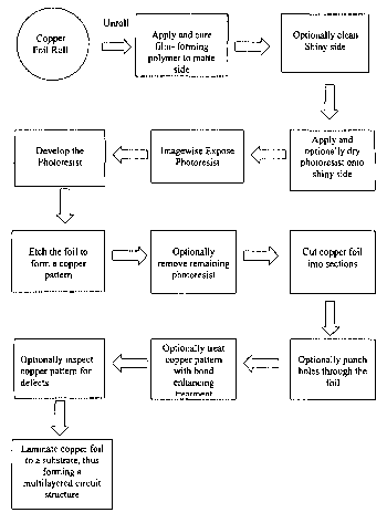
(a) unrolling a roll of copper foil, which foil has a shiny surface side and a
matte surface side;
(b) applying and curing a film-forming polymer onto the matte side of the
foil,
(c) optionally cleaning the shiny side of the foil;
(d) applying and optionally drying a photoresist onto the shiny side of the
foil;
(e) imagewise exposing the photoresist to actinic radiation to thereby form
image and nonimage areas;
(f) developing the photoresist thereby removing the nonimage areas and
leaving the image areas;
(g) etching the foil under the removed nonimage areas of the photoresist to
thereby form a copper pattern;
(h) optionally removing the remaining photoresist;
(i) cutting the foil into sections;
(j) optionally punching registration holes through the foil;
(lc) optionally treating the copper pattern with a bond enhancing treatment;
(1) optionally inspecting the copper pattern for defects; and
(m) laminating at least one foil section to a substrate; thus forming a
multilayered circuit structure.
The invention also provides a continuous process for forming a multilayered
circuit structure v~hich comprises:
(a) unrolling a roll of copper foil, which foil has a shiny surface side and a
matte surface side;
(b) applying and curing a film-forming polymer onto the matte side of the
foil,
4
CA 02432936 2003-06-23
WO 02/052910 PCT/USO1/47653
(c) cleaning the shiny side of the foil;
(d) applying and drying a photoresist onto the shiny side of the foil;
(e) imagewise exposing the photoresist to actinic radiation to thereby form
image and nonimage areas;
(f) developing the photoresist thereby removing the nonimage areas and
leaving the image areas;
(g) etching the foil under the removed nonimage areas of the photoresist to
thereby form a copper pattern;
(h) removing the remaining photoresist;
(i) cutting the foil into sections;
(j) punching registration holes through the foil;
(lc) treating the copper pattern with a bond enhancing treatment;
(1) inspecting the copper pattern for defects; and
(m) laminating at least one foil section to a substrate; thus forming a
multilayered circuit structure.
The invention further provides a continuous process for forming a
multilayered circuit structure which comprises:
(a) unrolling a roll of copper foil, which foil has a shiny surface side and a
matte surface side, both sides having been treated with bond enhancing
treatment;
(b) applying and curing a film-forming polymer onto either side of the foil,
(c) optionally cleaning the side of the foil that has not been applied with
the
film-forming polymer;
(d) applying and optionally drying a photoresist onto the uncoated side of the
foil;
(e) imagewise exposing the photoresist to actinic radiation to thereby form
image and nonimage areas;
(f) developing the photoresist thereby removing the nonimage axeas and
leaving the image areas;
5
CA 02432936 2003-06-23
WO 02/052910 PCT/USO1/47653
(g) etching the foil under the removed nonimage areas of the photoresist to
thereby form a copper pattern;
(h) optionally removing the remaining photoresist;
(i) cutting the foil into sections;
(j) optionally punching registration holes through the foil;
(1t) optionally inspecting the copper pattern for defects; and
(1) laminating at least one foil section to a substrate; thus forming a
multilayered circuit structure.
The invention still further provides a continuous process for forming a
multilayered circuit structure which comprises:
(a) unrolling a roll of copper foil, which foil has a shiny surface side and a
matte~surface side, whose shiny side has been treated with a bond enhancing
treatment;
(b) applying and curing a film-forming polymer onto the shiny side of the
foil,
(c) optionally cleaning the matte side of the foil;
(d) applying and optionally drying a photoresist onto the shiny side of the
foil;
(e) imagewise exposing the photoresist to actinic radiation to thereby form
image and nonimage areas;
(f) developing the photoresist thereby removing the nonimage areas and
leaving the image areas;
(g) etching the foil under the removed nonimage areas of the photoresist to
thereby form a copper pattern;
(h) optionally removing the remaining photoresist;
(i) cutting the foil into sections;
(j) optionally punching registration holes through the foil;
(k) optionally treating the copper pattern with a bond enhancing treatment;
(1) optionally inspecting the copper pattern for defects; and
(m) laminating at least one foil section to a substrate; thus forming a
multilayered circuit structure.
6
CA 02432936 2003-06-23
WO 02/052910 PCT/USO1/47653
BRIEF DESCRIPTION OF THE DRAWINGS
FIG.1 shows a flow chart representing the process steps according to the
invention.
DETAILED DESCRIPTION OF THE PREFERRED EMBODIMENT
The invention provides a continuous process for producing a multilayered
circuit structure. The process of the present invention is preferably
conducted
in a reel to reel manner.
The first step in one embodiment of the present invention is to unroll a roll
of
copper foil having a shiny surface side and a matte surface side. According to
the invention, the term "copper foil" preferably comprises copper or a copper
alloy. Copper alloys may contain zinc, chrome, nickel, aluminum, stainless
steel, iron, 'titanium and combinations thereof. Copper foils can be
manufactured by well lalown electrodeposition processes. One preferred
process includes electrodepositing copper from a solution of a copper salt
onto
a rotating metal drum. The side of the foil next to the drum is typically the
smooth or shiny side, while the other side has a relatively rough surface,
also
l~nown as the matte side. This drum is usually made of stainless steel or
titanium which acts as a cathode and receives the copper as it is deposited
from solution. An anode is generally constructed from a lead alloy. A cell
voltage of about 5 to 10 volts is applied between the anode and the cathode to
cause the copper to be deposited, while oxygen is evolved at the anode. This
copper foil is then removed from the drum.
The foil's shiny side, matte side, or both, may optionally be pre-treated with
a
bond enhancing treatment known in the art, which may serve as an adhesion
7
CA 02432936 2003-06-23
WO 02/052910 PCT/USO1/47653
promoter for the copper foil. One preferred bond enhancing treatment
includes Durabond, a tin oxide, which can be purchased commercially from
McGean Rohco Inc. of Cleveland, Ohio. Other suitable bond enhancing
treatments also nonexclusively include oxide treatments. One preferred oxide
treatment is black oxide treatment, which oxidizes the copper foil with an
oxidant thereby to convert the copper on the substrate to spiny copper oxide.
Black oxide treatment preferably uses, as a treating solution, a solution of
an
oxidant such as sodium hypochlorite. Since the oxidant solution is alkaline,
copper foils treated with the oxidant solution may need to be washed after the
treatment. One supplier of this chemistry is Electrochemicals Inc. of Maple
Plains, MN.
A film forming polymer composition is then applied and cured onto one side
of the foil. It is preferred that the film forming polymer composition is
applied and cured onto a side of the foil which has been pre-treated with a
bond enhancing treatment. This may be done to either side of the foil,
preferably the matte side. In an embodiment where both sides of the foil have
been pre-treated with a bond enhancing treatment as described above, then the
polymer composition may be applied and cured onto either side of the foil.
The copper foil is preferably partially or fully unrolled prior to the
application
and curing of the film forming polymer composition. Suitable film forming
polymers nonexclusively include polyimides, polyesters, polyester containing
co-polymers, polyarylene ethers, liquid crystal polymers, polyphenylene
ethers, amines, and combinations thereof. Of these, polyimides and polyesters
are the most preferred. The film forming polymer composition may optionally
contain a filler. The film forming polymer composition may be applied by
conventional techniques such as spraying, meniscus coating, doctoring blade
coating, sputtering, evaporation, vapor deposition or the lilce to allow for
control and uniformity of the polymer thickness. The polymer is then
preferably cured onto the foil, thus forming a prepreg. Curing is preferably
CA 02432936 2003-06-23
WO 02/052910 PCT/USO1/47653
conducted by conventional techniques such as heating in an oven. Preferably,
heat curing is performed at a temperature of from about 100°F to about
600°F,
for about 1 to about 10 minutes. After curing, the copper foil may be re-
rolled
for inspection and/or storage and unrolled at a later time for completion of
subsequent steps according to the invention. Such re-rolling and unrolling
may be done by any suitable method known in the art, such as by using an
accumulator.
Next, the side of the foil which has not been applied with the film forming
polymer may optionally be cleaned using conventional techniques. In an
embodiment where the matte side has been applied with the polymer, then the
shiny side may optionally be cleaned. Conversely, in an embodiment where
the shiny side has been applied with the polymer, then the matte side may
optionally be cleaned. It is preferred that the foil is partially or fully
unrolled
prior to cleaning. Cleaning may be done by any conventional method known
in the art, such as micro-etching with sodium persulfate or rinsing with mild
sulfuric acid.
Next, a photoresist is applied and optionally but preferably dried, onto the
side
of the foil opposite to that applied with the polymer. The photoresist
composition may be positive working or negative working and is generally
commercially available. Suitable positive working photoresists are well
known in the art and may comprise an o-quinone diazide radiation sensitizer.
The o-quinone diazide sensitizers include the o-quinone-4-or-5-sulfonyl-
diazides disclosed in U. S. Patents Nos. 2,797,213; 3,106,465; 3,148,983;
3,130,047; 3,201,329; 3,785,825; and 3,802,885. When o-quinone diazides
are used, preferred binding resins include a water insoluble, aqueous alkaline
soluble or swellable binding resin, which is preferably a novolalc. Suitable
positive photodielectric resins may be obtained commercially, for example,
under the trade name of AZ-P4620 from Clariant Corporation of Somerville,
9
CA 02432936 2003-06-23
WO 02/052910 PCT/USO1/47653
New Jersey as well as Shipley I-line photoresist. Negative photoresists are
also widely commercially available. The photoresist is preferably applied
onto the shiny side of the foil by conventional techniques such as mentioned
above. The thickness of photoresist layers may vary depending on the
deposition procedure used. The photoresist may then optionally be dried onto
the foil by conventional techniques such as heating. After applying and
optionally drying the photoresist onto the foil, the copper foil may be re-
rolled
for inspection and/or storage and unrolled at a later time for completion of
subsequent steps according to the invention. Such re-rolling and unrolling
may be done by any suitable method known in the art, such as using an
accumulator.
The photoresist is then imagewise exposed to actinic radiation such as light
in
the visible, ultraviolet or infrared regions of the spectrum through a mask,
or
scanned by an electron beam, ion or neutron beam or X-ray radiation, to
thereby form image and nonimage areas. The foil should be unrolled prior to
exposure. Actinic radiation may be in the form of incoherent light or coherent
light, for example, light from a laser. In one embodiment, the process of the
invention may be temporarily or permanently stopped after exposure of the
photoresisf to radiation.
The photoresist is then imagewise developed using a suitable solvent, such as
an aqueous alkaline solution, thereby removing the nonimage areas and
leaving the image areas. Preferred solvent developers are widely
commercially available and may comprise aqueous sodium hydroxide,
potassium hydroxide or sodium carbonate solutions.
The next step is to selectively etch away portions of the copper foil under
the
removed nonimage areas of the photoresist layer, forming an etched copper
pattern. This photoresist pattern defines an excellent quality etch mask for
CA 02432936 2003-06-23
WO 02/052910 PCT/USO1/47653
etching the conductive layer with high accuracy and precision. This etched
pattern may be formed by conventional techniques such as acid etching and
allcaline etching. Suitable etchants non-exclusively include alkaline
solutions
or acidic solutions, such as cupric chloride or nitric acid. Also preferred
are
ferric chloride or sulfuric peroxide. The remaining photoresist may then
optionally be removed using conventional techniques such as stripping or
ashing. In one embodiment, the process of the present invention may be
temporarily or permanently stopped after removal of the photoresist.
The foil is then cut preferably into sections by conventional techniques. The
sections are preferably squares, but may be any other shape necessary for a
particular application or process. Registration holes may then optionally be
punctured through the foil. The holes are preferably made using a punch
system, however any other method laiown in the art may alternatively be used.
It is preferred that the registration holes are punched prior to lamination of
the
foil.
Next, the copper pattern may be optionally treated with a bond enhancing
treatment, which serves as an adhesion promoter for the copper foil to the
bonding material (such as a fiberglass cloth coated with epoxy resin) .
The next step accor ding to the invention is the lamination the foil to a
substrate. Prior to lamination, the copper pattern may optionally be inspected
for defects. The optional inspection may be conducted by any suitable method
known in the art. Preferred methods nonexclusively include in-line optical
inspection,~random sampling, electrical testing, and visual inspection.
According to the invention, at least one foil section is laminated to a
substrate,
thus forming a multilayered circuit structure. In the practice of the
invention,
a plurality of foil sections may be laminated together. Also, a plurality of
the
11
CA 02432936 2003-06-23
WO 02/052910 PCT/USO1/47653
foil sections may be laminated together via a substrate between adjacent
sections. Lamination is preferably conducted in a press at a temperature of
from about 160°C to about 320°C, more preferably from about
170°C to
about 245°C and most preferably from about 175°C to about
230°C .
Lamination time preferably ranges from about 15 minutes to about 180
minutes, more preferably from about 30 minutes to about 120 minutes, and
most preferably from about 30 minutes to about 90 minutes. Preferably, the
press is under a vacuum of from at least 25 to about 30 mm of mercury, more
preferably from about 28 to about 30 mm of mercury, and most preferably
from about 29 to about 30 inches of mercury. The press pressure is preferably
maintained at about 3.5 to about 70 lcg/cm2, more preferably from about 7 to
about 30 lcg/cm2, and most preferably from about 9 lcg/cm2 to about 21
lcg/cm2.
Typical substrates are those suitable to be processed into a printed circuit
or
other microelectronic device. Suitable substrates for the present invention
non-exclusively include epoxies, polyimides, polyesters, cyanate ester, BT-
Epoxy or combinations thereof, polymers reinforced with materials such as
fiberglass, organic paper, aramid (Kevlar), aramid paper (Thermount),
polybenzoxolate paper or combinations thereof. Qf these, epoxy with
fiberglass reinforcement is the most preferred substrate. The preferred
thickness of the substrate is of from about 10 to about 200 ~.m, more
preferably from about 10 to about 50 ~,m.
In one embodiment of the present invention, the optional steps of cleaning the
foil, drying the photoresist, removing the remaining photoresist, punching
registration holes thiough the foil, treating the copper pattern with a bond
enhancing treatment, and inspecting the copper pattern for defects are all
performed.
12
CA 02432936 2003-06-23
WO 02/052910 PCT/USO1/47653
In another embodiment, particularly when using a foil where both the sides
have been subj ected to bond enhancing treatment, the optional step of
treating
the copper pattern with a bond enhancing treatment is not performed.
In still another embodiment, prior to lamination the copper foil may be
electrolytically treated on the shiny side to form a roughening copper
deposit,
and electrolytically treated on the matte side to deposit micro-nodules of a
metal or alloy. These nodules axe preferably copper or a copper alloy, and .
increase adhesion to a substrate. The surface microstructure of the foil is
measured by a profilometer, such as a Perthometer model M4P or SSP which
is commercially available from Mater Feinpruef Corporation of Cincinnati,
Ohio. Topography measurements of the surface grain structure of peaks and
valleys are made according to industry standaxd IPC-TM-650 Section 2.2.17
of the Institute for Interconnecting and Paclcaging Circuits of 2115 Sanders
Road, Northbroolc, Illinois 60062. In the measurement procedure, a
measurement length Im over the sample surface is selected. Rz defined as the
average maximum peals to valley height of five consecutive sampling lengths
within the measurement length Im (where Io is Im/5). Rt is the maximum
roughness depth and is the greatest perpendicular distance between the highest
peals and the lowest valley within the measurement length Im. Rp is the
maximum leveling depth and is the height of the highest pear within the
measuring length Im. Ra, or average roughness, is defined as the arithmetic
average value of all absolute distances of the roughness profile from the
center
line within the measuring length Im. The parameters of importance for this
invention are Rz and Ra. The surface treatments carried out produce a surface
structure having peaks and valleys, which produce roughness parameters
wherein Ra ranges from about 1 to about 10 ~,m and Rz ranges from about 2 to
about 10 ~,m.
13
CA 02432936 2003-06-23
WO 02/052910 PCT/USO1/47653
The surface treatments carried out produce a surface structure having peaks
and valleys, on the shiny side, which produce roughness parameters wherein
Ra ranges from about 1 to about 4 ~.m, preferably from about 2 to about 4
microns, and most preferably from about 3 to about 4 microns. The Rz value
ranges from about 2 to about 4.5 Vim, preferably from about 2.5 to about 4.5
microns, and more preferably from about 3 to about 4.5 ~,m.
The surface treatments carried out produce a surface structure having peaks
and valleys, on the matte side, which produce roughness parameters wherein
Ra ranges from about 4 to about 10 ~,m, preferably from about 4.5 to about 8
yn, and most preferably from about 5 to about 7.5 ~,m. The Rz value ranges
from about 4 to about 10 Vim, preferably from about 4 to about 9 Vim, and
more preferably from about 4 to about 7.5 Vim.
Preferably, the shiny side has a copper deposit about 2 to 4.5 ~m thiclc to
produce an average roughness (Rz) of 2 ~m or greater. More preferably, the
matte side preferably will have a roughness Rz as made of about 4-7.5 Vim.
The micro-nodules of metal or alloy will have a size of about 0.5 Vim. Other
metals may be deposited as micro nodules if desired, for example, zinc,
indium, tin, cobalt, brass, bronze and the like. This process is more
thoroughly described in U.S. patent 5,679,230, which is incorporated herein
by reference.
The shiny surface preferably has a peel strength ranging from about .7
lcg/linear cm to about 1.6 lcg/linear, more preferably fiom about .9
lcg/linear
cm to about 1.6 lcg/linear. The matte surface preferably has a peel strength
ranging from about .9 lcg/linear cm to about 2 lcg/linear, more preferably
from
about 1.1 kg/linear cm to about 2 lcg/linear. Peel strength is measured
according to industry standard IPC-TM-650 Section 2.4.~ Revision C.
14
CA 02432936 2003-06-23
WO 02/052910 PCT/USO1/47653
The following non-limiting examples serve to illustrate the invention. It will
be appreciated that variations in proportions and alternatives in elements of
the
components of the photosensitive coating composition will be apparent to
those skilled in the art and are within the scope of the present invention.
RXAMPT.R 1
A roll of electrodeposited 35 p,m, one ounce copper foil, 0.64 meters in width
is mounted on an unwind roller. The foil is threaded through tensioning
rollers, through idler rollers, and onto a rewind roller. The foil is then
tensioned to 4 pounds per inch width. A drive motor on the rewind roller is
engaged and set to 1.2 meters/minute. A liquid polyimide resin is adjusted to
25% solids, a viscosity of about 20,000 centipose, with N-methylpyrrolidone
in a stainless steel mixing vat. The polyimide solution is supplied to a
dispensing system and a film of approximately 50 yn is applied to the matte
side of the moving foil using gravity and the liquid polymer viscosity as
dispensing forces.
A doctor blade is adjusted to produce a wet film of 43 ~m in thickness,
resulting in a flexible composite having a dried polymer film in thicltness of
about 7.6 ~,m. A continuous liquid head height and volume of dammed
material is maintained on the upstream side of the doctor blade to maintain a
constant flexible composite film thickness and a film free of included air
bubbles.
The solvent is evaporated off and the polymer is cured in an oven at
425°C.
As the coated foil first enters the oven, an initial temperature drop should
be
anticipated. Once steady state temperatures are achieved in the oven, film
thickness is checked by taking a foil sample and comparing the coated weight
to the base weight of the foil using the polyimide density to convert from
CA 02432936 2003-06-23
WO 02/052910 PCT/USO1/47653
weight to film thickness. Adjustments to the rate of polyimide dispensed and
or doctor blade height over the foil are made based on this measurement. This
process is repeated until the desired film thickness is attained.
The shiny side of the foil is then cleaned and micro-etched with sodium
persulfate, followed by a water rinse and application of a photosensitive
resist.
The photoresist is dried and imagewise exposed through a mask to actinic
radiation using a UV exposure unit to thereby form image and nonimage
areas. The.photoresist is then developed using an aqueous sodium carbonate
solution to remove the nonimage areas and leaving the image areas. The foil
is then etched in cupric chloride to form a copper pattern. The balance of the
resist is stripped away using potassium hydroxide leaving the desired copper
pattern.
The foil is cut into rectangular sections which are then punched with tooling
holes using a optically registering mechanical punch . The copper pattern on
the foil sections is then treated with a solution containing 31 g/1 of sodium
hydrochlorite, 15 g/1 of sodium hydroxide and 12 g/1 of trisodium phosphate,
at 85°C under agitation for 3 minutes thereby to provide a black oxide
treatment.
The treated foil section is then laminated to an epoxy substrate reinforced
with
fiberglass, in a hydraulic press at 275 °C and 10 kg/cm2 for 30
minutes. The
press is under vacuum of 28 inches of mercury. A second foil section is
laminated to the first foil section to thereby form a multilayered circuit
structure.
EXAMPLE 2
Example l .is repeated except that the step black oxide treatment is conducted
16
CA 02432936 2003-06-23
WO 02/052910 PCT/USO1/47653
by dipping the copper foil for three minutes in an aqueous black oxide
treatment solution at 85 °C having the following composition:
NaC102 --31 g/1
NaOH--15 g/1
Na3P04 -_ 12 g/1
EXAMPLE 3
Example 1 is repeated except a 10 ~.~m sheet of p-phenylene-2,6-
benzobisoxazole paper is laminated between the polyimide surfaces of the foil
sections on the substrate. Resulting product has improved dimensional
stability and tear resistance.
EXAMPLE 4
Example l .is repeated except lamination is done using a continuous hot roll
lamination process at 300°C and 21 l~glcm2 . The product is subjected
to a
post lamination oven bake to achieve final cure.
EXAMPLE 5
Example 1 is repeated except coating is done with an extrusion coater and
lamination is done by a nip roller process. A filler is coextruded with the
polyimide.
EXAMPLE 6
Example 1 is repeated except the matte side of the foil is treated with
nodules
17
CA 02432936 2003-06-23
WO 02/052910 PCT/USO1/47653
to improve mechanical adhesion to the polyimide. Maximum nodule size is
less than 120 micro-inches to avoid the possibility of high potential
failures.
EXAMPLE 7
Example 1 is repeated except that a fiberglass cloth is impregnated with a non-
halogenated thermosetting polyimide (Keramid 601), forming a prepreg. The
polymer is then partially cured. The thicl~ness of this prepreg is about 68
p,m.
The copper foil is then laminated to the prepreg with the polymer coating
facing the prepreg. The lamination is done under a vacuum (28 inches of Hg)
at 275 °C, with 14 lcg/cm2 of pressure for 90 minutes.
EXAMPLE 8
Example 7 is repeated except a non-halogenated epoxy replaces the
thermosetting polyimide. The lamination is conducted at 185 °C for 60
minutes.
EXAMPLE 9
Example 7 is repeated except the substrate is another fiberglass and the
prepreg thiclcness is about 115 ~.m.
While the present invention has been particularly shown and described with
reference to preferred embodiments, it will be readily appreciated by those of
ordinary shill in the art that various changes and modifications may be made
without departing from the spirit and scope of the invention. It is intended
that
the claims be interpreted to cover the disclosed embodiment, those
alternatives
which have been discussed above and all equivalents thereto.
18