Note: Descriptions are shown in the official language in which they were submitted.
CA 02433144 2003-06-26
WO 02/058537 PCT/US01/50832
1
ANALYTE MONITORING DEVICE AND METHODS OF USE
Field of the Invention
The present invention is, in general, directed to devices and methods for the
in vivo monitoring of an analyte, such as glucose or lactate. More
particularly, the
present invention relates to devices and methods for the in vivo monitoring of
an
analyte using an electrochemical sensor to provide information to a patient
about the
level of the analyte.
Background of the Invention
The monitoring of the level of glucose or other analytes, such as lactate or
oxygen, in certain individuals is vitally important to their health. High or
low levels
of glucose or other analytes may have detrimental effects. The monitoring of
glucose is particularly important to individuals with diabetes, as they must
determine
when insulin is needed to reduce glucose levels in their bodies or when
additional
glucose is needed to raise the level of glucose in their bodies.
A conventional technique used by many diabetics for personally monitoring
their blood glucose level includes the periodic drawing of blood, the
application of
that blood to a test strip, and the determination of the blood glucose level
using
colorimetric, electrochemical, or photometric detection. This technique does
not
pelinit continuous or automatic monitoring of glucose levels in the body, but
typically must be performed manually on a periodic basis. Unfortunately, the
consistency with which the level of glucose is checked varies widely among
individuals. Many diabetics find the periodic testing inconvenient and they
sometimes forget to test their glucose level or do not have time for a proper
test. In
addition, some individuals wish to avoid the pain associated with the test.
These
situations may result in hyperglycemic or hypoglycemic episodes. An in vivo
glucose sensor that continuously or automatically monitors the individual's
glucose
level would enable individuals to more easily monitor their glucose, or other
analyte,
levels.
A variety of devices have been developed for continuous or automatic
monitoring of analytes, such as glucose, in the blood stream or interstitial
fluid. A
CA 02433144 2003-06-26
WO 02/058537 PCT/US01/50832
2
number of these devices use electrochemical sensors which are directly
implanted
into a blood vessel or in the subcutaneous tissue of a patient. However, these
devices are often difficult to reproducibly and inexpensively manufacture in
large
numbers. In addition, these devices are typically large, bully, and/or
inflexible, and
many can not be used effectively outside of a controlled medical facility,
such as a
hospital or a doctor's office, unless the patient is restricted in his
activities.
Some devices include a sensor guide which rests on or near the skin of the
patient and may be attached to the patient to hold the sensor in place. These
sensor
guides are typically bulky and do not allow for freedom of movement. In
addition,
the sensor guides or the sensors include cables or wires for connecting the
sensor to
other equipment to direct the signals from the sensors to an analyzer. The
size of the
sensor guides and presence of cables and wires hinders the convenient use of
these
devices for everyday applications. There is a need for a small, compact device
that
can operate the sensor and provide signals to an analyzer without
substantially
restricting the movements and activities of a patient.
The patient's comfort and the range of activities that can be perfoimed while
the sensor is implanted are important considerations in designing extended-use
sensors for continuous or automatic in vivo monitoring of the level of an
analyte,
such as glucose. There is a need for a small, comfortable device which can
continuously monitor the level of an analyte, such as glucose, while still
permitting
the patient to engage in normal activities. Continuous and/or automatic
monitoring
of the analyte can provide a warning to the patient when the level of the
analyte is at
or near a threshold level. For example, if glucose is the analyte, then the
monitoring
device might be configured to warn the patient of current or impending
hyperglycemia or hypoglycemia. The patient can then take appropriate actions.
Summary of the Invention
Generally, the present invention relates to methods and devices for the
continuous and/or automatic in vivo monitoring of the level of an analyte
using a
subcutaneously implantable sensor. Many of these devices are small and
comfortable when used, thereby allowing a wide range of activities. One
embodiment is a sensor control unit having a housing adapted for placement on
skin.
CA 02433144 2003-06-26
WO 02/058537
PCT/US01/50832
3
The housing is also adapted to receive a portion of an electrochemical sensor.
The
sensor control unit includes two or more conductive contacts disposed on the
housing and configured for coupling to two or more contact pads on the sensor.
A
transmitter is disposed in the housing and coupled to the plurality of
conductive
contacts for transmitting data obtained using the sensor. The sensor control
unit may
also include a variety of optional components, such as, for example, adhesive
for
adhering to the skin, a mounting unit, a receiver, a processing circuit, a
power supply
(e.g., a battery), an alarm system, a data storage unit, a watchdog circuit,
and a
measurement circuit. Other optional components are described below.
Another embodiment of the invention is a sensor assembly that includes the
sensor control unit described above. The sensor assembly also includes a
sensor
having at least one working electrode and at least one contact pad coupled to
the
working electrode or electrodes. The sensor may also include optional
components,
such as, for example, a counter electrode, a counter/reference electrode, a
reference
electrode, and a temperature probe. Other components and options for the
sensor are
described below.
A further embodiment of the invention is an analyte monitoring system that
includes the sensor control unit described above. The analyte monitoring
system
also includes a sensor that has at least one working electrode and at least
one contact
pad coupled to the working electrode or electrodes. The analyte monitoring
system
also includes a display unit that has a receiver for receiving data from the
sensor
control unit and a display coupled to the receiver for displaying an
indication of the
level of an analyte. The display unit may optionally include a variety of
components, such as, for example, a transmitter, an analyzer, a data storage
unit, a
watchdog circuit, an input device, a power supply, a clock, a lamp, a pager, a
telephone interface, a computer interface, an alarm or alarm system, a radio,
and a
calibration unit. Further components and options for the display unit are
described
below. In addition, the analyte monitoring system or a component of the
analyte
monitoring system may optionally include a processor capable of determining a
drug
or treatment protocol and/or a drug delivery system.
Yet another embodiment of the invention is an insertion kit for inserting an
electrochemical sensor into a patient. The insertion kit includes an inserter.
A
CA 02433144 2003-06-26
WO 02/058537 PCT/US01/50832
4
portion of the inserter has a sharp, rigid, planer structure adapted to
support the
sensor during insertion of the electrochemical sensor. The insertion kit also
includes
an insertion gun having a port configured to accept the electrochemical sensor
and
the inserter. The insertion gun has a driving mechanism for driving the
inserter and
electrochemical sensor into the patient, and a retraction mechanism for
removing the
inserter while leaving the sensor within the patient.
Another embodiment is a method of using an electrochemical sensor. A
mounting unit is adhered to skin of a patient. An insertion gun is aligned
with a port
on the mounting unit. The electrochemical sensor is disposed within the
insertion
gun and then the electrochemical sensor is inserted into the skin of the
patient using
the insertion gun. The insertion gun is removed and a housing of the sensor
control
unit is mounted on the mounting base. A plurality of conductive contacts
disposed
on the housing is coupled to a plurality of contact pads disposed on the
electrochemical sensor to prepare the sensor for use.
One embodiment of the invention is a method for detecting failures in an
implanted analyte-responsive sensor. An analyte-responsive sensor is implanted
into
a patient. The analyte-responsive sensor includes N working electrodes, where
N is
an integer and is two or greater, and a common counter electrode. Signals
generated
at one of the N working electrodes and at the common counter electrode are
then
obtained and the sensor is determined to have failed if the signal from the
common
counter electrode is not N times the signal from one of the working
electrodes,
within a predetermined threshold limit.
Yet another embodiment is a method of calibrating an electrochemical sensor
having one or more working electrodes implanted in a patient. A signal is
generated
from each of the working electrodes. Several conditions are tested to
deteimine if
calibration is appropriate. First, the signals from each of the one or more
working
electrodes should differ by less than a first threshold amount. Second, the
signals
from each of the one or more working electrodes should be within a
predetermined
range. And, third, a rate of change of the signals from each of the one or
more
working electrodes should be less than a second threshold amount. A
calibration
value is found assaying a calibration sample of a patient's body fluid. The
CA 02433144 2003-06-26
WO 02/058537 PCT/US01/50832
calibration value is then related to at least one of the signals from the one
or more
working electrodes if the conditions described above are met.
A further embodiment is a method for monitoring a level of an analyte. A
sensor is inserted into a skin of a patient and a sensor control unit is
attached to the
5 skin of the patient. Two or more conductive contacts on the sensor
control unit are
coupled to contact pads on the sensor. Then, using the sensor control unit,
data is
collected regarding a level of an analyte from signals generated by the
sensor. The
collected data is transmitted to a display unit and an indication of the level
of the
analyte is displayed on the display unit.
The above summary of the present invention is not intended to describe each
disclosed embodiment or every implementation of the present invention. The
Figures and the detailed description which follow more particularly exemplify
these
embodiments.
Brief Description of the Drawings
The invention may be more completely understood in consideration of the
following detailed description of various embodiments of the invention in
connection with the accompanying drawings, in which:
Figure 1 is a block diagram of one embodiment of a subcutaneous analyte
monitor using a subcutaneously implantable analyte sensor, according to the
invention;
Figure 2 is a top view of one embodiment of an analyte sensor, according to
the invention;
Figure 3A is a cross-sectional view of the analyte sensor of Figure 2;
Figure 3B is a cross-sectional view of another embodiment of an analyte
sensor, according to the invention;
Figure 4A is a cross-sectional view of a third embodiment of an analyte
sensor, according to the invention;
Figure 4B is a cross-sectional view of a fourth embodiment of an analyte
sensor, according to the invention;
Figure 5 is an expanded top view of a tip portion of the analyte sensor of
Figure 2;
CA 02433144 2003-06-26
WO 02/058537 PCT/US01/50832
6
Figure 6 is a cross-sectional view of a fifth embodiment of an analyte sensor,
according to the invention;
Figure 7 is an expanded top view of a tip-portion of the analyte sensor of
Figure 6;
Figure 8 is an expanded bottom view of a tip-portion of the analyte sensor of
Figure 6;
Figure 9 is a side view of the analyte sensor of Figure 2;
Figure 10 is a top view of the analyte sensor of Figure 6;
Figure 11 is a bottom view of the analyte sensor of Figure 6;
Figure 12 is an expanded side view of one embodiment of a sensor and an
insertion device, according to the invention;
Figures 13A, 13B, 13C are cross-sectional views of three embodiments of
the insertion device of Figure 12;
Figure 14 is a cross-sectional view of one embodiment of a on-skin sensor
control unit, according to the invention;
Figure 15 is a top view of a base of the on-skin sensor control unit of Figure
14;
Figure 16 is a bottom view of a cover of the on-skin sensor control unit of
Figure 14;
Figure 17 is a perspective view of the on-skin sensor control unit of Figure
14 on the skin of a patient;
Figure 18A is a block diagram of one embodiment of an on-skin sensor
control unit, according to the invention;
Figure 18B is a block diagram of another embodiment of an on-skin sensor
control unit, according to the invention;
Figures 19A, 19B, 19C, and 19D are cross-sectional views of four
embodiments of conductive contacts disposed on an interior surface of a
housing of
an on-skin sensor control unit, according to the invention;
Figures 19E and 19F are cross-sectional views of two embodiments of
conductive contacts disposed on an exterior surface of a housing of an on-skin
sensor control unit, according to the invention;
CA 02433144 2003-06-26
WO 02/058537 PCT/US01/50832
7
Figures 20A and 20B are schematic diagrams of two embodiments of a
current-to-voltage converter for use in an analyte monitoring device,
according to
the invention;
Figure 21 is a block diagram of one embodiment of an open loop modulation
system for use in an analyte monitoring device, according to the invention;
Figure 22 is a block diagram of one embodiment of a receiver/display unit,
according to the invention;
Figure 23 is a front view of one embodiment of a receiver/display unit;
Figure 24 is a front view of a second embodiment of a receiver/display unit;
Figure 25 is a block diagram of one embodiment of a drug delivery system,
according to the invention;
Figure 26 is a perspective view of the internal structure of an insertion gun,
according to the invention;
Figure 27A is a top view of one embodiment of an on-skin sensor control
unit, according to the invention;
Figure 27B is a top view of one embodiment of a mounting unit of the on-
skin sensor control unit of Figure 27A;
Figure 28A is a top view of another embodiment of an on-skin sensor control
unit after insertion of an insertion device and a sensor, according to the
invention;
Figure 28B is a top view of one embodiment of a mounting unit of the oil-
skin sensor control unit of Figure 28A;
Figure 28C is a top view of one embodiment of a housing for at least a
portion of the electronics of the on-skin sensor control unit of Figure 28A;
Figure 28D is a bottom view of the housing of Figure 28C; and
Figure 28E is a top view of the on-skin sensor control unit of Figure 28A
with a cover of the housing removed.
Figure 29 depicts two sensor current-analyte level profiles at differing
temperatures.
Figure 30 depicts three code division multiple access (CDMA) transmitters
simultaneously transmitting across a transmission medium to a CDMA receiver.
Figure 31 depicts a data message that may be transmitted under an
interleaved transmission scheme.
CA 02433144 2003-06-26
WO 02/058537 PCT/US01/50832
8
Figure 32 depicts one possible embodiment of a transmitter disposed upon a
substrate.
Figure 33 depicts an insertion device, sensor, insertion gun and mounting
unit, which can be assembled and sold together in an insertion kit
While the invention is amenable to various modifications and alternative
forms, specifics thereof have been shown by way of example in the drawings and
will be described in detail. It should be understood, however, that the
intention is
not to limit the invention to the particular embodiments described. On the
contrary,
the intention is to cover all modifications, equivalents, and alternatives
falling within
the spirit and scope of the invention as defined by the appended claims.
Detailed Description of the Invention
The present invention is applicable to an analyte monitoring system using an
implantable sensor for the in vivo determination of a concentration of an
analyte,
such as glucose or lactate, in a fluid. The sensor can be, for example,
subcutaneously
implanted in a patient for the continuous or periodic monitoring an analyte in
a
patient's interstitial fluid. This can then be used to infer the glucose level
in the
patient's bloodstream. Other in vivo analyte sensors can be made, according to
the
invention, for insertion into a vein, artery, or other portion of the body
containing
fluid. The analyte monitoring system is typically configured for monitoring
the
level of the analyte over a time period which may range from days to weeks or
longer.
The following definitions are provided for terms used herein:
A "counter electrode" refers to an electrode paired with the working
electrode, through which passes a current equal in magnitude and opposite in
sign to
the current passing through the working electrode. In the context of the
invention,
the term "counter electrode" is meant to include counter electrodes which also
function as reference electrodes (i.e., a counter/reference electrode).
An "electrochemical sensor" is a device configured to detect the presence
and/or measure the level of an analyte in a sample via electrochemical
oxidation and
reduction reactions on the sensor. These reactions are transduced to an
electrical
CA 02433144 2003-06-26
WO 02/058537 PCT/US01/50832
9
signal that can be correlated to an amount, concentration, or level of an
analyte in the
sample.
"Electrolysis" is the electrooxidation or electroreduction of a compound
either directly at an electrode or via one or more electron transfer agents.
A compound is "immobilized" on a surface when it is entrapped on or
chemically bound to the surface.
A "non-leachable" or "non-releasable" compound or a compound that is
"non-leachably disposed" is meant to define a compound that is affixed on the
sensor such that it does not substantially diffuse away from the working
surface of
the working electrode for the period in which the sensor is used (e.g., the
period in
which the sensor is implanted in a patient or measuring a sample).
Components are "immobilized" within a sensor, for example, when the
components are covalently, ionically, or coordinatively bound to constituents
of the
sensor and/or are entrapped in a polymeric or sol-gel matrix or membrane which
precludes mobility.
An "electron transfer agent" is a compound that carries electrons between the
analyte and the working electrode, either directly, or in cooperation with
other
electron transfer agents. One example of an electron transfer agent is a redox
mediator.
A "working electrode" is an electrode at which the analyte (or a second
compound whose level depends on the level of the analyte) is electrooxidized
or
electroreduced with or without the agency of an electron transfer agent.
A "working surface" is that portion of the working electrode which is coated
with or is accessible to the electron transfer agent and configured for
exposure to an
analyte-containing fluid.
A "sensing layer" is a component of the sensor which includes constituents
that facilitate the electrolysis of the analyte. The sensing layer may include
constituents such as an electron transfer agent, a catalyst which catalyzes a
reaction
of the analyte to produce a response at the electrode, or both. In some
embodiments
of the sensor, the sensing layer is non-leachably disposed in proximity to or
on the
working electrode.
-
CA 02433144 2009-03-03
WO 02/058537 PCT/US01/50832
A "non-corroding" conductive material includes non-metallic materials, such
as carbon and conductive polymers.
Analyte Sensor Systems
5 The analyte monitoring systems of the present invention can be
utilized =
under a variety of conditions. The particular configuration of a sensor and
other
units used in the analyte monitoring system may depend on the use for which
the
analyte monitoring system is intended and the conditions under which the
analyte
monitoring system will operate. One embodiment of the analyte monitoring
system
10 includes a sensor configured for implantation into a patient or user.
For example,
implantation of the sensor may be made in the arterial or venous systems for
direct
testing of analyte levels in blood. Alternatively, a sensor may be implanted
in the
interstitial tissue for determining the analyte level in interstitial fluid.
This level
may be correlated and/or converted to analyte levels in blood or other fluids.
The
site and depth of implantation may affect the particular shape, components,
and
configuration of the sensor. Subcutaneous implantation may be preferred, in
some
cases, to limit the depth of implantation of the sensor. Sensors may also be
implanted in other regions of the body to determine analyte levels in other
fluids..
Examples of suitable sensor for use in the analyte monitoring systems of the
invention are described in U.S. Patent No. 6,134,461 issued 17 October, 2000.
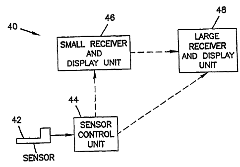
One embodiment of the analyte monitoring system 40 for use with an
implantable sensor 42, and particularly for use with a subcutaneously
implantable
sensor, is illustrated in block diagram form in Figure 1. The analyte
monitoring
system 40 includes, at minimum, a sensor 42, a portion of which is configured
for
implantation (e.g., subcutaneous, venous, or arterial implantation) into a
patient, and
a sensor control unit 44. The sensor 42 is coupled to the sensor control unit
44
which is typically attached to the skin of a patient. The sensor control unit
44
operates the sensor 42, including, for example, providing a voltage across the
electrodes of the sensor 42 and collecting signals from the sensor 42. The
sensor
control unit 44 may evaluate the signals from the sensor 42 and/or transmit
the
signals to one or more optional receiver/display units 46, 48 for evaluation.
The
CA 02433144 2009-03-03
WO 02/058537 PCT/US01/50832
11
sensor control unit 44 and/or the receiver/display units 46, 48 may display or
otherwise communicate the current level of the analyte. Furthermore, the
sensor
control unit 44 and/or the receiver/display units 46, 48 may indicate to the
patient,
via, for example, an audible, visual, or other sensory-stimulating alarm, when
the
level of the analyte is at or near a threshold level. In some embodiments, a
electrical
shock can be delivered to the patient as a warning through one of the
electrodes or
the optional temperature probe of the sensor. For example, if glucose is
monitored
then an alann may be used to alert the patient to a hypoglycemic or
hyperglycemic
=
glucose level and/or to impending hypoglycemia or hyperglycemia.
The Sensor
= A sensor 42 includes at least one working electrode 58 formed on a
substrate
50, as shown in Figure 2. The sensor 42 may also include at least one counter
electrode 60 (or counter/reference electrode) and/or at least one reference
electrode
62 (see Figure 8). The counter electrode 60 and/or reference electrode 62 may
be
formed on the substrate 50 or may be separate units. For example, the counter
electrode and/or reference electrode may be formed on a second substrate which
is
= also implanted in the patient or, for some embodiments of the implantable
sensors,
the counter electrode and/or reference electrode may be placed on the skin of
the
patient with the working electrode or electrodes being implanted into the
patient.
The use of an on-the-skin counter and/or reference electrode with an
implantable
working electrode is described in U.S. Patent No. 5,593,852 issued 14 January,
1997.
The working electrode or electrodes 58 are formed using conductive traces
52 disposed on the substrate 50. The counter electrode 60 and/or reference
electrode
62, as well as other optional portions of the sensor 42, such as a temperature
probe
66 (see Figure 8), may also be formed using conductive traces 52 disposed on
the
substrate 50. These conductive traces 52 may be formed over a smooth surface
of
the substrate 50 or within channels 54 formed by, for example, embossing,
indenting
or otherwise creating a depression in the substrate 50.
A sensing layer 64 (see Figures 3A and 3B) is often formed proximate to or
on at least one of the working electrodes 58 to facilitate the electrochemical
7
CA 02433144 2003-06-26
WO 02/058537 PCT/US01/50832
12
detection of the analyte and the determination of its level in the sample
fluid,
particularly if the analyte can not be electrolyzed at a desired rate and/or
with a
desired specificity on a bare electrode. The sensing layer 64 may include an
electron
transfer agent to transfer electrons directly or indirectly between the
analyte and the
working electrode 58. The sensing layer 64 may also contain a catalyst to
catalyze a
reaction of the analyte. The components of the sensing layer may be in a fluid
or gel
that is proximate to or in contact with the working electrode 58.
Alternatively, the
components of the sensing layer 64 may be disposed in a polymeric or sol-gel
matrix
that is proximate to or on the working electrode 58. Preferably, the
components of
the sensing layer 64 are non-leachably disposed within the sensor 42. More
preferably, the components of the sensor 42 are immobilized within the sensor
42.
In addition to the electrodes 58, 60, 62 and the sensing layer 64, the sensor
42 may also include a temperature probe 66 (see Figures 6 and 8), a mass
transport
limiting layer 74 (see Figure 9), a biocompatible layer 75 (see Figure 9),
and/or other
optional components, as described below. Each of these items enhances the
functioning of and/or results from the sensor 42, as discussed below.
The Substrate
The substrate 50 may be formed using a variety of non-conducting materials,
including, for example, polymeric or plastic materials and ceramic materials.
Suitable materials for a particular sensor 42 may be determined, at least in
part,
based on the desired use of the sensor 42 and properties of the materials.
In some embodiments, the substrate is flexible. For example, if the sensor 42
is configured for implantation into a patient, then the sensor 42 may be made
flexible (although rigid sensors may also be used for implantable sensors) to
reduce
pain to the patient and damage to the tissue caused by the implantation of
and/or the
wearing of the sensor 42. A flexible substrate 50 often increases the
patient's
comfort and allows a wider range of activities. Suitable materials for a
flexible
substrate 50 include, for example, non-conducting plastic or polymeric
materials and
other non-conducting, flexible, deformable materials. Examples of useful
plastic or
polymeric materials include theimoplastics such as polycarbonates, polyesters
(e.g.,
MylarTM and polyethylene terephthalate (PET)), polyvinyl chloride (PVC),
CA 02433144 2003-06-26
WO 02/058537 PCT/US01/50832
13
polyurethanes, polyethers, polyamides, polyimides, or copolymers of these
thermoplastics, such as PETG (glycol-modified polyethylene terephthalate).
In other embodiments, the sensors 42 are made using a relatively rigid
substrate 50 to, for example, provide structural support against bending or
breaking.
Examples of rigid materials that may be used as the substrate 50 include
poorly
conducting ceramics, such as aluminum oxide and silicon dioxide. One advantage
of an implantable sensor 42 having a rigid substrate is that the sensor 42 may
have a
sharp point and/or a sharp edge to aid in implantation of a sensor 42 without
an
additional insertion device.
It will be appreciated that for many sensors 42 and sensor applications, both
rigid and flexible sensors will operate adequately. The flexibility of the
sensor 42
may also be controlled and varied along a continuum by changing, for example,
the
composition and/or thickness of the substrate 50.
In addition to considerations regarding flexibility, it is often desirable
that
implantable sensors 42 should have a substrate 50 which is non-toxic.
Preferably,
the substrate 50 is approved by one or more appropriate governmental agencies
or
private groups for in vivo use.
The sensor 42 may include optional features to facilitate insertion of an
implantable sensor 42, as shown in Figure 12. For example, the sensor 42 may
be
pointed at the tip 123 to ease insertion. In addition, the sensor 42 may
include a barb
125 which assists in anchoring the sensor 42 within the tissue of the patient
during
operation of the sensor 42. However, the barb 125 is typically small enough
that
little damage is caused to the subcutaneous tissue when the sensor 42 is
removed for
replacement.
Although the substrate 50 in at least some embodiments has uniform
dimensions along the entire length of the sensor 42, in other embodiments, the
substrate 50 has a distal end 67 and a proximal end 65 with different widths
53, 55,
respectively, as illustrated in Figure 2. In these embodiments, the distal end
67 of
the substrate 50 may have a relatively nan-ow width 53. For sensors 42 which
are
implantable into the subcutaneous tissue or another portion of a patient's
body, the
narrow width 53 of the distal end 67 of the substrate 50 may facilitate the
CA 02433144 2003-06-26
WO 02/058537 PCT/US01/50832
14
implantation of the sensor 42. Often, the narrower the width of the sensor 42,
the
less pain the patient will feel during implantation of the sensor and
afterwards.
For subcutaneously implantable sensors 42 which are designed for
continuous or periodic monitoring of the analyte during normal activities of
the
patient, a distal end 67 of the sensor 42 which is to be implanted into the
patient has
a width 53 of 2mm or less, preferably lmm or less, and more preferably 0.5mm
or
less. If the sensor 42 does not have regions of different widths, then the
sensor 42
will typically have an overall width of, for example, 2 mm, 1.5 mm, 1 mm, 0.5
mm,
0.25 min, or less. However, wider or narrower sensors may be used. In
particular,
wider implantable sensors may be used for insertion into veins or arteries or
when
the movement of the patient is limited, for example, when the patient is
confined in
bed or in a hospital.
Returning to Figure 2, the proximal end 65 of the sensor 42 may have a
width 55 larger than the distal end 67 to facilitate the connection between
contact
pads 49 of the electrodes and contacts on a control unit. The wider the sensor
42 at
this point, the larger the contact pads 49 can be made. This may reduce the
precision
needed to properly connect the sensor 42 to contacts on the control unit
(e.g., sensor
control unit 44 of Figure 1). However, the maximum width of the sensor 42 may
be
constrained so that the sensor 42 remains small for the convenience and
comfort of
the patient and/or to fit the desired size of the analyte monitor. For
example, the
proximal end 65 of a subcutaneously implantable sensor 42, such as the sensor
42
illustrated in Figure 1, may have a width 55 ranging from 0.5mm to 15mm,
preferably from lmm to lOmm, and more preferably from 3mm to 7mm. However,
wider or narrower sensors may be used in this and other in vivo applications.
The thickness of the substrate 50 may be determined by the mechanical
properties of the substrate material (e.g., the strength, modulus, and/or
flexibility of
the material), the desired use of the sensor 42 including stresses on the
substrate 50
arising from that use, as well as the depth of any channels or indentations
formed in
the substrate 50, as discussed below. Typically, the substrate 50 of a
subcutaneously
implantable sensor 42 for continuous or periodic monitoring of the level of an
analyte while the patient engages in normal activities has a thickness of 50
to 500
CA 02433144 2003-06-26
WO 02/058537 PCT/US01/50832
ium and preferably 100 to 300 m. However, thicker and thinner substrates 50
may
be used, particularly in other types of in vivo sensors 42.
The length of the sensor 42 may have a wide range of values depending on a
variety of factors. Factors which influence the length of an implantable
sensor 42
5 may include the depth of implantation into the patient and the ability of
the patient to
manipulate a small flexible sensor 42 and make connections between the sensor
42
and the sensor control unit 44. A subcutaneously implantable sensor 42 for the
analyte monitor illustrated in Figure 1 may have a length ranging from 0.3 to
5 cm,
however, longer or shorter sensors may be used. The length of the narrow
portion of
10 the sensor 42 (e.g., the portion which is subcutaneously inserted into
the patient), if
the sensor 42 has narrow and wide portions, is typically about 0.25 to 2 cm in
length.
However, longer and shorter portions may be used. All or only a part of this
narrow
portion may be subcutaneously implanted into the patient. The lengths of other
implantable sensors 42 will vary depending, at least in part, on the portion
of the
15 patient into which the sensor 42 is to be implanted or inserted.
Conductive Traces
At least one conductive trace 52 is formed on the substrate for use in
constructing a working electrode 58. In addition, other conductive traces 52
may be
formed on the substrate 50 for use as electrodes (e.g., additional working
electrodes,
as well as counter, counter/reference, and/or reference electrodes) and other
components, such as a temperature probe. The conductive traces 52 may extend
most of the distance along a length 57 of the sensor 50, as illustrated in
Figure 2,
although this is not necessary. The placement of the conductive traces 52 may
depend on the particular configuration of the analyte monitoring system (e.g.,
the
placement of control unit contacts and/or the sample chamber in relation to
the
sensor 42). For implantable sensors, particularly subcutaneously implantable
sensors, the conductive traces typically extend close to the tip of the sensor
42 to
minimize the amount of the sensor that must be implanted.
The conductive traces 52 may be formed on the substrate 50 by a variety of
techniques, including, for example, photolithography, screen printing, or
other
impact or non-impact printing techniques. The conductive traces 52 may also be
-
CA 02433144 2009-03-03
WO 02/058537 PCT/US01/50832
16
formed by carbonizing conductive traces 52 in an organic (e.g., polymeric or
plastic)
substrate 50 using a laser. A description of some exemplary methods for
forming
the sensor 42 is provided in U.S. Patent No. 6,103,033 issued 15 August, 2000.
Another method for disposing the conductive traces 52 on the substrate 50
includes the formation of recessed channels 54 in one or more surfaces of the
substrate 50 and the subsequent filling of these recessed channels 54 with a
conductive material 56, as shown in Figure 3A. The recessed channels 54 may be
formed by indenting, embossing, or otherwise creating a depression in the
surface of
the substrate 50. Exemplary methods for forming channels and electrodes in a
. surface of a substrate can be found in U.S. Patent No. 6,103,033.
The depth of the channels is typically related to the thickness of the
substrate 50. In
one embodiment, the channels have depths in the range of about 12.5 to 75 pm (
0.5
to 3 mils), and preferably about 25 to 50 Inn (1 to 2 mils).
The conductive traces are typically formed using a conductive material 56
such as carbon (e.g., graphite), a conductive polymer, a metal or alloy (e.g.,
gold or
gold alloy), or a metallic compound (e.g., ruthenium dioxide or titanium
dioxide).
The formation of films of carbon, conductive polymer, metal, alloy, or
metallic
compound are well-known and include, for example, chemical vapor deposition
(CVD), physical vapor deposition, sputtering, reactive sputtering, printing,
coating,
and painting. The conductive material 56 which fills the channels 54 is often
formed
using a precursor material, such as a conductive ink or paste. In these
embodiments,
the conductive material 56 is deposited on the substrate 50 using methods such
as
coating, painting, or applying the material using a spreading instrument, such
as a
coating blade. Excess conductive material between the channels 54 is then
removed
by, for example, running a blade along the substrate surface.
In one embodiment, the conductive material 56 is a part of a precursor
material, such as a conductive ink, obtainable, for example, from Ercon, Inc.
(Wareham, MA), Metech, Inc. (Elverson, PA), E.I. du Pont de Nemours and Co.
(Wilmington, DE), Emca-Remex Products (Montgomeryville, PA), or MCA
Services (Melbourn, Great Britain). The conductive ink is typically applied as
a
semiliquid or paste which contains particles of the carbon, metal, alloy, or
metallic
WeA I ====
CA 02433144 2003-06-26
WO 02/058537 PCT/US01/50832
17
,
compound and a solvent or dispersant. After application of the conductive ink
on
the substrate 50 (e.g., in the channels 54), the solvent or dispersant
evaporates to
leave behind a solid mass of conductive material 56.
In addition to the particles of carbon, metal, alloy, or metallic compound,
the
conductive ink may also contain a binder. The binder may optionally be cured
to
further bind the conductive material 56 within the channel 54 and/or on the
substrate
50. Curing the binder increases the conductivity of the conductive material
56.
However, this is typically not necessary as the currents carried by the
conductive
material 56 within the conductive traces 52 are often relatively low (usually
less than
1 IAA and often less than 100 nA). Typical binders include, for example,
polyurethane resins, cellulose derivatives, elastomers, and highly fluorinated
polymers. Examples of elastomers include silicones, polymeric dienes, and
acrylonitrile-butadiene-styrene (ABS) resins. One example of a fluorinated
polymer
binder is Teflon (DuPont, Wilmington, DE). These binders are cured using, for
example, heat or light, including ultraviolet (UV) light. The appropriate
curing
method typically depends on the particular binder which is used.
Often, when a liquid or semiliquid precursor of the conductive material 56
(e.g., a conductive ink) is deposited in the channel 54, the precursor fills
the channel
54. However, when the solvent or dispersant evaporates, the conductive
material 56
which remains may lose volume such that the conductive material 56 may or may
not continue to fill the channel 54. Preferred conductive materials 56 do not
pull
away from the substrate 50 as they lose volume, but rather decrease in height
within
the channel 54. These conductive materials 56 typically adhere well to the
substrate
50 and therefore do not pull away from the substrate 50 during evaporation of
the
solvent or dispersant. Other suitable conductive materials 56 either adhere to
at least
a portion of the substrate 50 and/or contain another additive, such as a
binder, which
adheres the conductive material 56 to the substrate 50. Preferably, the
conductive
material 56 in the channels 54 is non-leachable, and more preferably
immobilized on
the substrate 50. In some embodiments, the conductive material 56 may be
formed
by multiple applications of a liquid or semiliquid precursor interspersed with
removal of the solvent or dispersant.
CA 02433144 2003-06-26
WO 02/058537 PCT/US01/50832
18
In another embodiment, the channels 54 are formed using a laser. The laser
carbonizes the polymer or plastic material. The carbon formed in this process
is
used as the conductive material 56. Additional conductive material 56, such as
a
conductive carbon ink, may be used to supplement the carbon formed by the
laser.
In a further embodiment, the conductive traces 52 are fOrmed by pad printing
techniques. For example, a film of conductive material is formed either as a
continuous film or as a coating layer deposited on a carrier film. This film
of
conductive material is brought between a print head and the substrate 50. A
pattern
on the surface of the substrate 50 is made using the print head according to a
desired
pattern of conductive traces 52. The conductive material is transferred by
pressure
and/or heat from the film of conductive material to the substrate 50. This
technique
often produces channels (e.g., depressions caused by the print head) in the
substrate
50. Alternatively, the conductive material is deposited on the surface of the
substrate 50 without forming substantial depressions.
In other embodiments, the conductive traces 52 are formed by non-impact
printing techniques. Such techniques include electrophotography and
magneto graphy. In these processes, an image of the conductive traces 52 is
electrically or magnetically formed on a drum. A laser or LED may be used to
electrically form an image. A magnetic recording head may be used to
magnetically
form an image. A toner material (e.g., a conductive material, such as a
conductive
ink) is then attracted to portions of the drum according to the image. The
toner
material is then applied to the substrate by contact between the drum and the
substrate. For example, the substrate may be rolled over the drum. The toner
material may then be dried and/or a binder in the toner material may be cured
to
adhere the toner material to the substrate.
Another non-impact printing technique includes ejecting droplets of
conductive material onto the substrate in a desired pattern. Examples of this
technique include ink jet printing and piezo jet printing. An image is sent to
the
printer which then ejects the conductive material (e.g., a conductive ink)
according
to the pattern. The printer may provide a continuous stream of conductive
material
or the printer may eject the conductive material in discrete amounts at the
desired
points.
CA 02433144 2003-06-26
WO 02/058537
PCT/US01/50832
19
Yet another non-impact printing embodiment of forming the conductive
traces includes an ionographic process. In the this process, a curable, liquid
precursor, such as a photopolymerizable acrylic resin (e.g., Solimer 7501 from
Cubital, Bad Kreuznach, Germany) is deposited over a surface of a substrate
50. A
photomask having a positive or negative image of the conductive traces 52 is
then
used to cure the liquid precursor. Light (e.g., visible or ultraviolet light)
is directed
through the photomask to cure the liquid precursor and form a solid layer over
the
substrate according to the image on the photomask. Uncured liquid precursor is
removed leaving behind channels 54 in the solid layer. These channels 54 can
then
be filled with conductive material 56 to form conductive traces 52.
Conductive traces 52 (and channels 54, if used) can be founed with relatively
narrow widths, for example, in the range of 25 to 250 tim, and including
widths of,
for example, 250pm, 150 pm, 100 pm, 75 pm, 501.tm, 25pm or less by the methods
described above. In embodiments with two or more conductive traces 52 on the
same side of the substrate 50, the conductive traces 52 are separated by
distances
sufficient to prevent conduction between the conductive traces 52. The edge-to-
edge
distance between the conductive traces is preferably in the range of 25 to 250
m and
may be, for example, 150 i.tm, 100 pm, 751tm, 50 pm, or less. The density of
the
conductive traces 52 on the substrate 50 is preferably in the range of about
150 to
700 m/trace and may be as small as 667 p.m/trace or less, 333 m/trace or
less, or
even 167 m/trace or less.
The working electrode 58 and the counter electrode 60 (if a separate
reference electrode is used) are often made using a conductive material 56,
such as
carbon. Suitable carbon conductive inks are available from Ercon, Inc.
(Wareham,
MA), Metech, Inc. (Elverson, PA), E.I. du Pont de Nemours and Co. (Wilmington,
DE), Emca-Remex Products (Montgomeryville, PA), or MCA Services (Melboum,
Great Britain). Typically, the working surface 51 of the working electrode 58
is at
least a portion of the conductive trace 52 that is in contact with the analyte-
containing fluid (e.g., implanted in the patient).
The reference electrode 62 and/or counter/reference electrode are typically
formed using conductive material 56 that is a suitable reference material, for
example silver/silver chloride or a non-leachable redox couple bound to a
conductive
CA 02433144 2003-06-26
WO 02/058537 PCT/US01/50832
material, for example, a carbon-bound redox couple. Suitable silver/silver
chloride
conductive inks are available from Ercon, Inc. (Wareham, MA), Metech, Inc.
(Elverson, PA), E.I. du Pont de Nemours and Co. (Wilmington, DE), Emca-Remex
Products (Montgomeryville, PA), or MCA Services (Melboum, Great Britain).
5 Silver/silver chloride electrodes illustrate a type of reference
electrode that involves
the reaction of a metal electrode with a constituent of the sample or body
fluid, in
this case, Cr.
Suitable redox couples for binding to the conductive material of the reference
electrode include, for example, redox polymers (e.g., polymers having multiple
10 redox centers.) It is preferred that the reference electrode surface be
non-corroding
so that an erroneous potential is not measured. Preferred conductive materials
include less corrosive metals, such as gold and palladium. Most preferred are
non-
corrosive materials including non-metallic conductors, such as carbon and
conducting polymers. A redox polymer can be adsorbed on or covalently bound to
15 the conductive material of the reference electrode, such as a carbon
surface of a
conductive trace 52. Non-polymeric redox couples can be similarly bound to
carbon
or gold surfaces.
A variety of methods may be used to immobilize a redox polymer on an
electrode surface. One method is adsorptive immobilization. This method is
20 particularly useful for redox polymers with relatively high molecular
weights. The
molecular weight of a polymer may be increased, for example, by cross-linking.
Another method for immobilizing the redox polymer includes the
functionalization of the electrode surface and then the chemical bonding,
often
covalently, of the redox polymer to the functional groups on the electrode
surface.
One example of this type of immobilization begins with a poly(4-
vinylpyridine).
The polymer's pyridine rings are, in part, complexed with a
reducible/oxidizable
species, such as [0s(bpy)2C1r where bpy is 2,2'-bipyridine. Part of the
pyridine
rings are quatemized by reaction with 2-bromoethylamine. The polymer is then
crosslinked, for example, using a diepoxide, such as polyethylene glycol
diglycidyl
ether.
Carbon surfaces can be modified for attachment of a redox species or
polymer, for example, by electroreduction of a diazonium salt. As an
illustration,
CA 02433144 2003-06-26
WO 02/058537 PCT/US01/50832
21
reduction of a diazonium salt formed upon diazotization of p-aminobenzoic acid
modifies a carbon surface with phenylcarboxylic acid functional groups. These
functional groups can then be activated by a carbodiimide, such as 1-ethy1-3-
(3-
dimethylaminopropy1)-carbodiimide hydrochloride. The activated functional
groups
are then bound with a amine-functionalized redox couple, such as the
quaternized
osmium-containing redox polymer described above or 2-aminoethylferrocene, to
form the redox couple.
Similarly, gold can be functionalized by an amine, such as cystamine,. A
redox couple such as [0s(bpy)2(pyridine-4-carboxylate)Clr is activated by 1-
ethyl-
3-(3-dimethylaminopropy1)-carbodiimide hydrochloride to form a reactive 0-
acylisourea which reacts with the gold-bound amine to form an amide.
In one embodiment, in addition to using the conductive traces 52 as
electrodes or probe leads, two or more of the conductive traces 52 on the
substrate
50 are used to give the patient a mild electrical shock when, for example, the
analyte
level exceeds a threshold level. This shock may act as a warning or alarm to
the
patient to initiate some action to restore the appropriate level of the
analyte.
The mild electrical shock is produced by applying a potential between any
two conductive traces 52 that are not otherwise connected by a conductive
path. For
example, two of the electrodes 58, 60, 62 or one electrode 58, 60, 62 and the
temperature probe 66 may be used to provide the mild shock. Preferably, the
working electrode 58 and the reference electrode 62 are not used for this
purpose as
this may cause some damage to the chemical components on or proximate to the
particular electrode (e.g., the sensing layer on the working electrode or the
redox
couple on the reference electrode).
The current used to produce the mild shock is typically 0.1 to I mA. Higher
or lower currents may be used, although care should be taken to avoid harm to
the
patient. The potential between the conductive traces is typically 1 to 10
volts.
However, higher or lower voltages may be used depending, for example, on the
resistance of the conductive traces 52, the distance between the conductive
traces 52
and the desired amount of current. When the mild shock is delivered,
potentials at
the working electrode 58 and across the temperature probe 66 may be removed to
prevent harm to those components caused by unwanted conduction between the
CA 02433144 2003-06-26
WO 02/058537 PCT/US01/50832
22
working electrode 58 (and/or temperature probe 66, if used) and the conductive
traces 52 which provide the mild shock.
Contact Pads
Typically, each of the conductive traces 52 includes a contact pad 49. The
contact pad 49 may simply be a portion of the conductive trace 52 that is
indistinguishable from the rest of the trace 52 except that the contact pad 49
is
brought into contact with the conductive contacts of a control unit (e.g., the
sensor
control unit 44 of Figure 1). More commonly, however, the contact pad 49 is a
region of the conductive trace 52 that has a larger width than other regions
of the
trace 52 to facilitate a connection with the contacts on the control unit. By
making
the contact pads 49 relatively large as compared with the width of the
conductive
traces 52, the need for precise registration between the contact pads 49 and
the
contacts on the control unit is less critical than with small contact pads.
The contact pads 49 are typically made using the same material as the
conductive material 56 of the conductive traces 52. However, this is not
necessary.
Although metal, alloys, and metallic compounds may be used to fotat the
contact
pads 49, in some embodiments, it is desirable to make the contact pads 49 from
a
carbon or other non-metallic material, such as a conducting polymer. In
contrast to
metal or alloy contact pads, carbon and other non-metallic contact pads are
not
easily corroded if the contact pads 49 are in a wet, moist, or humid
environment.
Metals and alloys may corrode under these conditions, particularly if the
contact
pads 49 and contacts of the control unit are made using different metals or
alloys.
However, carbon and non-metallic contact pads 49 do not significantly corrode,
even
if the contacts of the control device are metal or alloy.
One embodiment of the invention includes a sensor 42 having contact pads
49 and a control unit 44 having conductive contacts (not shown). During
operation
of the sensor 42, the contact pads 49 and conductive contacts are in contact
with
each other. In this embodiment, either the contact pads 49 or the conductive
contacts are made using a non-corroding, conductive material. Such materials
include, for example, carbon and conducting polymers. Preferred non-corroding
materials include graphite and vitreous carbon. The opposing contact pad or
CA 02433144 2003-06-26
WO 02/058537 PCT/US01/50832
23
conductive contact is made using carbon, a conducting polymer, a metal, such
as
gold, palladium, or platinum group metal, or a metallic compound, such as
ruthenium dioxide. This configuration of contact pads and conductive contacts
typically reduces corrosion. Preferably, when the sensor is placed in a 3 mM,
and
more preferably, in a 100 mM, NaCl solution, the signal arising due to the
corrosion
of the contact pads and/or conductive contacts is less than 3% of the signal
generated
by the sensor when exposed to concentration of analyte in the noinial
physiological
range. For at least some subcutaneous glucose sensors, the current generated
by
analyte in a normal physiological range ranges from 3 to 500 nA.
Each of the electrodes 58, 60, 62, as well as the two probe leads 68, 70 of
the
temperature probe 66 (described below), are connected to contact pads 49 as
shown
in Figures 10 and 11. In one embodiment (not shown), the contact pads 49 are
on
the same side of the substrate 50 as the respective electrodes or temperature
probe
leads to which the contact pads 49 are attached.
In other embodiments, the conductive traces 52 on at least one side are
connected through vias in the substrate to contact pads 49a on the opposite
surface
of the substrate 50, as shown in Figures 10 and 11. An advantage of this
configuration is that contact between the contacts on the control unit and
each of the
electrodes 58, 60, 62 and the probe leads 68,70 of the temperature probe 66
can be
made from a single side of the substrate 50.
In yet other embodiments (not shown), vias through the substrate are used to
provide contact pads on both sides of the substrate 50 for each conductive
trace 52.
The vias connecting the conductive traces 52 with the contact pads 49a can be
formed by making holes through the substrate 50 at the appropriate points and
then
filling the holes with conductive material 56.
Exemplary Electrode Configurations
A number of exemplary electrode configurations are described below,
however, it will be understood that other configurations may also be used. In
one
embodiment, illustrated in Figure 3A, the sensor 42 includes two working
electrodes
58a, 58b and one counter electrode 60, which also functions as a reference
electrode.
In another embodiment, the sensor includes one working electrode 58a, one
counter
CA 02433144 2003-06-26
WO 02/058537 PCT/US01/50832
24
electrode 60, and one reference electrode 62, as shown in Figure 3B. Each of
these
embodiments is illustrated with all of the electrodes formed on the same side
of the
substrate 50.
Alternatively, one or more of the electrodes may be formed on an opposing
side of the substrate 50. This may be convenient if the electrodes are formed
using
two different types of conductive material 56 (e.g., carbon and silver/silver
chloride).
Then, at least in some embodiments, only one type of conductive material 56
needs
to be applied to each side of the substrate 50, thereby reducing the number of
steps
in the manufacturing process and/or easing the registration constraints in the
process.
For example, if the working electrode 58 is formed using a carbon-based
conductive
material 56 and the reference or counter/reference electrode is formed using a
silver/silver chloride conductive material 56, then the working electrode and
reference or counter/reference electrode may be formed on opposing sides of
the
substrate 50 for ease of manufacture.
In another embodiment, two working electrodes 58 and one counter electrode
60 are formed on one side of the substrate 50 and one reference electrode 62
and a
temperature probe 66 are formed on an opposing side of the substrate 50, as
illustrated in Figure 6. The opposing sides of the tip of this embodiment of
the
sensor 42 are illustrated in Figures 7 and 8.
Sensing Layer
Some analytes, such as oxygen, can be directly electrooxidized or
electroreduced on the working electrode 58. Other analytes, such as glucose
and
lactate, require the presence of at least one electron transfer agent and/or
at least one
catalyst to facilitate the electrooxidation or electroreduction of the
analyte. Catalysts
may also be used for those analyte, such as oxygen, that can be directly
electrooxidized or electroreduced on the working electrode 58. For these
analytes,
each working electrode 58 has a sensing layer 64 formed proximate to or on a
working surface of the working electrode 58. Typically, the sensing layer 64
is
formed near or on only a small portion of the working electrode 58, often near
a tip
of the sensor 42. This limits the amount of material needed to form the sensor
42
CA 02433144 2009-03-03
WO 02/058537 PCT/US01/50832
and places the sensing layer 64 in the best position for contact with the
analyte-
containing fluid (e.g., a body fluid, sample fluid, or carrier fluid).
The sensing layer 64 includes one or more components designed to facilitate
the electrolysis of the analyte. The sensing layer 64 may include, for
example, a
5 catalyst to catalyze a reaction of the analyte and produce a response at
the working
electrode 58, an electron transfer agent to indirectly or directly transfer
electrons
between the analyte and the working electrode 58, or both.
The sensing layer 64 may be formed as a solid composition of the desired
components (e.g., an electron transfer agent and/or a catalyst). These
components
10 are preferably non-leachable from the sensor 42 and more preferably are
immobilized on the sensor 42. For example, the components may be immobilized
on a working electrode 58. Alternatively, the components of the sensing layer
64
may be immobilized within or between one or more membranes or films disposed
over the working electrode 58 or the components may be immobilized in a
15 polymeric or sol-gel matrix. Examples of immobilized sensing layers are
described
in U.S. Patents Nos. 5,262,035, 5,264,104, 5,264,105, 5,320,725, 5,593,852,
and
5,665,222 and PCT Patent Publication No. WO/1998/035053.
In some embodiments, one or more of the components of the sensing layer
=
64 may be solvated, dispersed, or suspended in a fluid within the sensing
layer 64,
instead of forming a solid composition. The fluid may be provided with the
sensor
42 or may be absorbed by the sensor 42 from the analyte-containing fluid.
Preferably, the components which are solvated, dispersed, or suspended in this
type
of sensing layer 64 are non-leachable from the sensing layer. Non-leachability
may
be accomplished, for example, by providing barriers(e.g., the electrode,
substrate,
membranes, and/or films) around the sensing layer which prevent the leaching
of
the components of the sensing layer 64. One example of such a barrier is a
microporous membrane or film which allows diffusion of the analyte into the
sensing layer 64 to make contact with the components of the sensing layer 64,
but
CA 02433144 2003-06-26
WO 02/058537 PCT/US01/50832
26
reduces or eliminates the diffusion of the sensing layer components (e.g., a
electron
transfer agent and/or a catalyst) out of the sensing layer 64.
A variety of different sensing layer configurations can be used. In one
embodiment, the sensing layer 64 is deposited on the conductive material 56 of
a
working electrode 58a, as illustrated in Figures 3A and 3B. The sensing layer
64
may extend beyond the conductive material 56 of the working electrode 58a. In
some cases, the sensing layer 64 may also extend over the counter electrode 60
or
reference electrode 62 without degrading the performance of the glucose
sensor. For
those sensors 42 which utilize channels 54 within which the conductive
material 56
is deposited, a portion of the sensing layer 64 may be formed within the
channel 54
if the conductive material 56 does not fill the channel 54.
A sensing layer 64 in direct contact with the working electrode 58a may
contain an electron transfer agent to transfer electrons directly or
indirectly between
the analyte and the working electrode, as well as a catalyst to facilitate a
reaction of
the analyte. For example, a glucose, lactate, or oxygen electrode may be
fauned
having a sensing layer which contains a catalyst, such as glucose oxidase,
lactate
oxidase, or laccase, respectively, and an electron transfer agent that
facilitates the
electrooxidation of the glucose, lactate, or oxygen, respectively.
In another embodiment, the sensing layer 64 is not deposited directly on the
working electrode 58a. Instead, the sensing layer 64 is spaced apart from the
working electrode 58a, as illustrated in Figure 4A, and separated from the
working
electrode 58a by a separation layer 61. The separation layer 61 typically
includes
one or more membranes or films. In addition to separating the working
electrode
58a from the sensing layer 64, the separation layer 61 may also act as a mass
transport limiting layer or an interferent eliminating layer, as described
below.
Typically, a sensing layer 64, which is not in direct contact with the working
electrode 58a, includes a catalyst that facilitates a reaction of the analyte.
However,
this sensing layer 64 typically does not include an electron transfer agent
that
transfers electrons directly from the working electrode 58a to the analyte, as
the
sensing layer 64 is spaced apart from the working electrode 58a. One example
of
this type of sensor is a glucose or lactate sensor which includes an enzyme
(e.g.,
glucose oxidase or lactate oxidase, respectively) in the sensing layer 64. The
CA 02433144 2009-03-03
WO 02/058537 PCT/US01/50832
27
glucose or lactate reacts with a second compound (e.g., oxygen) in the
presence of
the enzyme. The second compound is then electromddized or electroreduced at
the
electrode. Changes in the signal at the electrode indicate changes in the
level of the
second compound in the fluid and are proportional to changes in glucose or
lactate
level and, thus, correlate to the analyte level.
In another embodiment, two sensing layers 63, 64 are used, as shown in
Figure 4B. Each of the two sensing layers 63, 64 may be independently formed
on
the working electrode 58a or in proximity to the working electrode 58a. One
sensing layer 64 is typically, although not necessarily, spaced apart from the
working electrode 58a. For example, this sensing layer 64 may include a
catalyst
which catalyzes a reaction of the analyte to form a product compound. The
product
compound is then electrolyzed in the second sensing layer 63 which may include
an
electron transfer agent to transfer electrons between the working electrode
58a and
the product compound and/or a second catalyst to catalyze a reaction of the
product
compound to generate a signal at the working electrode 58a.
For example, a glucose or lactate sensor may include a first sensing layer 64
which is spaced apart from the working electrode and contains an enzyme, for
example, glucose oxidase or lactate oxidase. The reaction of glucose or
lactate in
the presence of the appropriate enzyme forms hydrogen peroxide. A second
sensing
layer 63 is provided directly on the working electrode 58a and contains a
peroxidase
enzyme and an electron transfer agent to generate a signal at the electrode in
response to the hydrogen peroxide. The level of hydrogen peroxide indicated by
the
sensor then correlates to the level of glucose or lactate. Another sensor
which
operates similarly can be made using a single sensing layer with both the
glucose or
lactate oxidase and the peroxidase being deposited in the single sensing
layer.
Examples of such sensors are described in U.S. Patent Nos. 5,593,852 and
5,665,222, and
PCT Publication No. WO/1998/035053.
In some embodiments, one or more of the working electrodes 58b do not
have a corresponding sensing layer 64, as shown in Figures 3A and 4A, or have
a sensing
layer (not shown) which does not contain one or more components (e.g., an
CA 02433144 2003-06-26
WO 02/058537 PCT/US01/50832
28
electron transfer agent or catalyst) needed to electrolyze the analyte. The
signal
generated at this working electrode 58b typically arises from interferents and
other
sources, such as ions, in the fluid, and not in response to the analyte
(because the
analyte is not electrooxidized or electroreduced). Thus, the signal at this
working
electrode 58b corresponds to a background signal. The background signal can be
removed from the analyte signal obtained from other working electrodes 58a
that are
associated with fully-functional sensing layers 64 by, for example,
subtracting the
signal at working electrode 58b from the signal at working electrode 58a.
Sensors having multiple working electrodes 58a may also be used to obtain
more precise results by averaging the signals or measurements generated at
these
working electrodes 58a. In addition, multiple readings at a single working
electrode
58a or at multiple working electrodes may be averaged to obtain more precise
data.
Electron Transfer Agent
In many embodiments, the sensing layer 64 contains one or more electron
transfer agents in contact with the conductive material 56 of the working
electrode
58, as shown in Figures 3A and 3B. In some embodiments of the invention, there
is
little or no leaching of the electron transfer agent away from the working
electrode
58 during the period in which the sensor 42 is implanted in the patient. A
diffusing
or leachable (i.e., releasable) electron transfer agent often diffuses into
the analyte-
containing fluid, thereby reducing the effectiveness of the electrode by
reducing the
sensitivity of the sensor over time. In addition, a diffusing or leaching
electron
transfer agent in an implantable sensor 42 may also cause damage to the
patient. In
these embodiments, preferably, at least 90%, more preferably, at least 95%,
and,
most preferably, at least 99%, of the electron transfer agent remains disposed
on the
sensor after immersion in the analyte-containing fluid for 24 hours, and, more
preferably, for 72 hours. In particular, for an implantable sensor,
preferably, at least
90%, more preferably, at least 95%, and most preferably, at least 99%, of the
electron transfer agent remains disposed on the sensor after immersion in the
body
fluid at 37 C for 24 hours, and, more preferably, for 72 hours.
In some embodiments of the invention, to prevent leaching, the electron
transfer agents are bound or otherwise immobilized on the working electrode 58
or
CA 02433144 2003-06-26
WO 02/058537 PCT/US01/50832
29
between or within one or more membranes or films disposed over the working
electrode 58. The electron transfer agent may be immobilized on the working
electrode 58 using, for example, a polymeric or sol-gel immobilization
technique.
Alternatively, the electron transfer agent may be chemically (e.g., ionically,
covalently, or coordinatively) bound to the working electrode 58, either
directly or
indirectly through another molecule, such as a polymer, that is in turn bound
to the
working electrode 58.
Application of the sensing layer 64 on a working electrode 58a is one method
for creating a working surface for the working electrode 58a, as shown in
Figures 3A
and 3B. The electron transfer agent mediates the transfer of electrons to
electrooxidin or electroreduce an analyte and thereby permits a current flow
between the working electrode 58 and the counter electrode 60 via the analyte.
The
mediation of the electron transfer agent facilitates the electrochemical
analysis of
analytes which are not suited for direct electrochemical reaction on an
electrode.
In general, the preferred electron transfer agents are electroreducible and
electrooxidizable ions or molecules having redox potentials that are a few
hundred
millivolts above or below the redox potential of the standard calomel
electrode
(SCE). Preferably, the electron transfer agents are not more reducing than
about -
150 mV and not more oxidizing than about +400 mV versus SCE.
The electron transfer agent may be organic, organometallic, or inorganic.
Examples of organic redox species are quinones and species that in their
oxidized
state have quinoid structures, such as Nile blue and indophenol. Some quinones
and
partially oxidized quinhydrones react with functional groups of proteins such
as the
thiol groups of cysteine, the amine groups of lysine and arginine, and the
phenolic
groups of tyrosine which may render those redox species unsuitable for some of
the
sensors of the present invention because of the presence of the interfering
proteins in
an analyte-containing fluid. Usually substituted quinones and molecules with
quinoid structure are less reactive with proteins and are preferred. A
preferred
tetrasubstituted quinone usually has carbon atoms in positions 1, 2, 3, and 4.
In general, electron transfer agents suitable for use in the invention have
structures or charges which prevent or substantially reduce the diffusional
loss of the
electron transfer agent during the period of time that the sample is being
analyzed.
CA 02433144 2009-03-03
WO 02/058537 PCT/US01/50832
The preferred electron transfer agents include a redox species bound to a
polymer
which can in turn be immobilized on the working electrode. The bond between
the
redox species and the polymer may be covalent, coordinative, or ionic. Useful
electron transfer agents and methods for producing them are described in U.S.
Patent
5 Nos. 5,264,104; 5,356,786; 5,262,035; and 5,320,725.
Although any organic or organometallic redox species can be bound to a
polymer and used as an electron transfer agent, the preferred redox species is
a
transition metal compound or complex. The preferred transition metal compounds
or complexes include osmium, ruthenium, iron, and cobalt compounds or
10 complexes. The most preferred are osmium compounds and complexes.
It will be
recognized that many of the redox species described below may also be used,
= typically without a polymeric component, as electron transfer agents in a
carrier
= fluid or in a sensing layer of a sensor where leaching of the electron
transfer agent is
acceptable.
15 One type of non-releasable polymeric electron transfer agent
contains a redox
species covalently bound in a polymeric composition. An example of this type
of
mediator is poly(vinylferrocene).
Another type of non-releasable electron transfer agent contains an ionically-
bound redox species. Typically, this type of mediator includes a charged
polymer
20 coupled to an oppositely charged redox species. Examples of this
type of mediator
include a negatively charged polymer such as Nafion (DuPont) coupled to a
positively charged redox species such as an osmium or ruthenium polypyridyl
cation. Another example of an ionically-bound mediator is a positively charged
polymer such as quaternized poly(4-vinyl pyridine) or poly(1-vinyl imidazole)
25 coupled to a negatively charged redox species such as ferricyanide
or ferrocyanide.
The preferred ionically-bound redox species is a highly charged redox species
bound
within an oppositely charged redox polymer.
In another embodiment of the invention, suitable non-releasable electron
transfer agents include a redox species coordinatively bound to a polymer. For
30 example, the mediator may be formed by coordination of an osmium or
cobalt 2, 2'-
bipyridyl complex to poly(1-vinyl imidazole) or poly(4-vinyl pyridine).
CA 02433144 2003-06-26
WO 02/058537 PCT/US01/50832
31
The preferred electron transfer agents are osmium transition metal complexes
with one or more ligands, each ligand having a nitrogen-containing heterocycle
such
as 2,2'-bipyridine, 1,10-phenanthroline, or derivatives thereof. Furthermore,
the
preferred electron transfer agents also have one or more ligands covalently
bound in
a polymer, each ligand having at least one nitrogen-containing heterocycle,
such as
pyridine, imidazole, or derivatives thereof. These preferred electron transfer
agents
exchange electrons rapidly between each other and the working electrodes 58 so
that
the complex can be rapidly oxidized and reduced.
One example of a particularly useful electron transfer agent includes (a) a
polymer or copolymer having pyridine or imidazole functional groups and (b)
osmium cations complexed with two ligands, each ligand containing 2,2'-
bipyridine,
1,10-phenanthroline, or derivatives thereof, the two ligands not necessarily
being the
same. Preferred derivatives of 2,2'-bipyridine for complexation with the
osmium
cation are 4,4'-dimethy1-2,2'-bipyridine and mono-, di-, and polyalkoxy-2,2'-
bipyridines, such as 4,4'-dimethoxy-2,2'-bipyridine. Preferred derivatives of
1,10-
phenanthroline for complexation with the osmium cation are 4,7-dimethy1-1,10-
phenanthroline and mono, di-, and polyalkoxy-1,10-phenanthrolines, such as 4,7-
dimethoxy-1,10-phenanthroline. Preferred polymers for complexation with the
osmium cation include polymers and copolymers of poly(1-vinyl imidazole)
(referred to as "PVI") and poly(4-vinyl pyridine) (referred to as "PVP").
Suitable
copolymer substituents of poly(1-vinyl imidazole) include acrylonitrile,
acrylamide,
and substituted or quaternized N-vinyl imidazole. Most preferred are electron
transfer agents with osmium complexed to a polymer or copolymer of poly(1-
vinyl
imidazole).
The preferred electron transfer agents have a redox potential ranging from -
100 mV to about +150 mV versus the standard calomel electrode (SCE).
Preferably,
the potential of the electron transfer agent ranges from -100 mV to +150 mV
and
more preferably, the potential ranges from -50 mV to +50 mV. The most
preferred
electron transfer agents have osmium redox centers and a redox potential
ranging
from +50 mV to -150 mV versus SCE.
Catalyst
CA 02433144 2003-06-26
WO 02/058537 PCT/US01/50832
32
The sensing layer 64 may also include a catalyst which is capable of
catalyzing a reaction of the analyte. The catalyst may also, in some
embodiments,
act as an electron transfer agent. One example of a suitable catalyst is an
enzyme
which catalyzes a reaction of the analyte. For example, a catalyst, such as a
glucose
oxidase, glucose dehydrogenase (e.g., pyrroloquinoline quinone glucose
dehydrogenase (PQQ)), or oligosaccharide dehydrogenase, may be used when the
analyte is glucose. A lactate oxidase or lactate dehydrogenase may be used
when the
analyte is lactate. Laccase may be used when the analyte is oxygen or when
oxygen
is generated or consumed in response to a reaction of the analyte.
Preferably, the catalyst is non-leachably disposed on the sensor, whether the
catalyst is part of a solid sensing layer in the sensor or solvated in a fluid
within the
sensing layer. More preferably, the catalyst is immobilized within the sensor
(e.g.,
on the electrode and/or within or between a membrane or film) to prevent
unwanted
leaching of the catalyst away from the working electrode 58 and into the
patient.
This may be accomplished, for example, by attaching the catalyst to a polymer,
cross
linking the catalyst with another electron transfer agent (which, as described
above,
can be polymeric), and/or providing one or more barrier membranes or films
with
pore sizes smaller than the catalyst.
As described above, a second catalyst may also be used. This second catalyst
is often used to catalyze a reaction of a product compound resulting from the
catalyzed reaction of the analyte. The second catalyst typically operates with
an
electron transfer agent to electrolyze the product compound to generate a
signal at
the working electrode. Alternatively, the second catalyst may be provided in
an
interferent-eliminating layer to catalyze reactions that remove interferents,
as
described below.
One embodiment of the invention is an electrochemical sensor in which the
catalyst is mixed or dispersed in the conductive material 56 which forms the
conductive trace 52 of a working electrode 58. This may be accomplished, for
example, by mixing a catalyst, such as an enzyme, in a carbon ink and applying
the
mixture into a channel 54 on the surface of the substrate 50. Preferably, the
catalyst
is immobilized in the channel 53 so that it can not leach away from the
working
electrode 58. This may be accomplished, for example, by curing a binder in the
CA 02433144 2003-06-26
WO 02/058537 PCT/US01/50832
33
carbon ink using a curing technique appropriate to the binder. Curing
techniques
include, for example, evaporation of a solvent or dispersant, exposure to
ultraviolet
light, or exposure to heat. Typically, the mixture is applied under conditions
that do
not substantially degrade the catalyst. For example, the catalyst may be an
enzyme
that is heat-sensitive. The enzyme and conductive material mixture should be
applied and cured, preferably, without sustained periods of heating. The
mixture
may be cured using evaporation or UV curing techniques or by the exposure to
heat
that is sufficiently short that the catalyst is not substantially degraded.
Another consideration for in vivo analyte sensors is the thermo stability of
the
catalyst. Many enzymes have only limited stability at biological temperatures.
Thus, it may be necessary to use large amounts of the catalyst and/or use a
catalyst
that is thermostable at the necessary temperature (e.g., 37 C or higher for
normal
body temperature). A thermostable catalyst may be defined as a catalyst which
loses
less than 5% of its activity when held at 37 C for at least one hour,
preferably, at
least one day, and more preferably at least three days. One example of a
thermostable catalyst is soybean peroxidase. This particular thermostable
catalyst
may be used in a glucose or lactate sensor when combined either in the same or
separate sensing layers with glucose or lactate oxidase or dehydrogenase. A
further
description of thermostable catalysts and their use in electrochemical
inventions is
found in U.S. Patent No. 5,665,222 U.S. Patent Application No. 08/540,789, and
PCT Application No. US98/02403 entitled "Soybean Percoddase Electrochemical
Sensor", filed on February 11, 1998, Attorney Docket No. M&G 12008.8W012.
Electrolysis of the Analyte
To electrolyze the analyte, a potential (versus a reference potential) is
applied
across the working and counter electrodes 58, 60. The minimum magnitude of the
applied potential is often dependent on the particular electron transfer
agent, analyte
(if the analyte is directly electrolyzed at the electrode), or second compound
(if a
second compound, such as oxygen or hydrogen peroxide, whose level is dependent
on the analyte level, is directly electrolyzed at the electrode). The applied
potential
usually equals or is more oxidizing or reducing, depending on the desired
electrochemical reaction, than the redox potential of the electron transfer
agent,
CA 02433144 2003-06-26
WO 02/058537 PCT/US01/50832
34
analyte, or second compound, whichever is directly electrolyzed at the
electrode.
The potential at the working electrode is typically large enough to drive the
electrochemical reaction to or near completion.
The magnitude of the potential may optionally be limited to prevent
significant (as determined by the current generated in response to the
analyte)
electrochemical reaction of interferents, such as urate, ascorb ate, and
acetaminophen. The limitation of the potential may be obviated if these
interferents
have been removed in another way, such as by providing an interferent-limiting
bather, as described below, or by including a working electrode 58b (see
Figure 3A)
=
from which a background signal may be obtained.
When a potential is applied between the working electrode 58 and the
counter electrode 60, an electrical current will flow. The current is a result
of the
electrolysis of the analyte or a second compound whose level is affected by
the
analyte. In one embodiment, the electrochemical reaction occurs via an
electron
transfer agent and the optional catalyst. Many analytes B are oxidized (or
reduced)
to products C by an electron transfer agent species A in the presence of an
appropriate catalyst (e.g., an enzyme). The electron transfer agent A is then
oxidized
(or reduced) at the electrode. Electrons are collected by (or removed from)
the
electrode and the resulting current is measured. This process is illustrated
by
reaction equations (1) and (2) (similar equations may be written for the
reduction of
the analyte B by a redox mediator A in the presence of a catalyst):
catalyst
nA(ox) + B ____________________________________ nA(red) + C (1)
electrode
nA(red) _____________________________________ > nA(ox) + ne" (2)
As an example, an electrochemical sensor may be based on the reaction of a
glucose molecule with two non-leachable ferricyanide anions in the presence of
glucose oxidase to produce two non-leachable ferrocyanide anions, two hydrogen
ions, and gluconolactone. The amount of glucose present is assayed by
electrooxidizing the non-leachable ferrocyanide anions to non-leachable
ferricyanide
anions and measuring the current.
CA 02433144 2003-06-26
WO 02/058537 PCT/US01/50832
In another embodiment, a second compound whose level is affected by the
analyte is electrolyzed at the working electrode. In some cases, the analyte D
and
the second compound, in this case, a reactant compound E, such as oxygen,
react in
the presence of the catalyst, as shown in reaction equation (3).
catalyst
5 D + E __________ >F + G (3)
The reactant compound E is then directly oxidized (or reduced) at the working
electrode, as shown in reaction equation (4)
electrode
nE(red) ______________________________ > nE(ox) + ne- (4)
Alternatively, the reactant compound E is indirectly oxidized (or reduced)
using an
10 electron transfer agent H (optionally in the presence of a catalyst),
that is
subsequently reduced or oxidized at the electrode, as shown in reaction
equations (5)
and (6).
nH(ox) + E __________________________ > nH(red) + I (5)
electrode
nH(red) ______________________________ > nH(ox) + ne- (6)
15 In either case, changes in the concentration of the reactant
compound, as
indicated by the signal at the working electrode, correspond inversely to
changes in
the analyte (i.e., as the level of analyte increase then the level of reactant
compound
and the signal at the electrode decreases.)
In other embodiments, the relevant second compound is a product compound
20 F, as shown in reaction equation (3). The product compound F is formed
by the
catalyzed reaction of analyte D and then be directly electrolyzed at the
electrode or
indirectly electrolyzed using an electron transfer agent and, optionally, a
catalyst. In
these embodiments, the signal arising from the direct or indirect electrolysis
of the
product compound F at the working electrode corresponds directly to the level
of the
CA 02433144 2003-06-26
WO 02/058537 PCT/US01/50832
36
analyte (unless there are other sources of the product compound). As the level
of
analyte increases, the level of the product compound and signal at the working
electrode increases.
Those skilled in the art will recognize that there are many different
reactions
that will achieve the same result; namely the electrolysis of an analyte or a
compound whose level depends on the level of the analyte. Reaction equations
(1)
through (6) illustrate non-limiting examples of such reactions.
Temperature Probe
A variety of optional items may be included in the sensor. One optional item
is a temperature probe 66 (Figures 8 and 11). The temperature probe 66 may be
made using a variety of known designs and materials. One exemplary temperature
probe 66 is formed using two probe leads 68, 70 connected to each other
through a
temperature-dependent element 72 that is formed using a material with a
temperature-dependent characteristic. An example of a suitable temperature-
dependent characteristic is the resistance of the temperature-dependent
element 72.
The two probe leads 68, 70 are typically formed using a metal, an alloy, a
semimetal, such as graphite, a degenerate or highly doped semiconductor, or a
small-
band gap semiconductor. Examples of suitable materials include gold, silver,
ruthenium oxide, titanium nitride, titanium dioxide, indium doped tin oxide,
tin
doped indium oxide, or graphite. The temperature-dependent element 72 is
typically
made using a fine trace (e.g., a conductive trace that has a smaller cross-
section than
that of the probe leads 68, 70) of the same conductive material as the probe
leads, or
another material such as a carbon ink, a carbon fiber, or platinum, which has
a
temperature-dependent characteristic, such as resistance, that provides a
temperature-dependent signal when a voltage source is attached to the two
probe
leads 68, 70 of the temperature probe 66. The temperature-dependent
characteristic
of the temperature-dependent element 72 may either increase or decrease with
temperature. Preferably, the temperature dependence of the characteristic of
the
temperature-dependent element 72 is approximately linear with temperature over
the
expected range of biological temperatures (about 25 to 45 C), although this
is not
required.
CA 02433144 2003-06-26
WO 02/058537 PCT/US01/50832
37
Typically, a signal (e.g., a current) having an amplitude or other property
that
is a function of the temperature can be obtained by providing a potential
across the
two probe leads 68, 70 of the temperature probe 66. As the temperature
changes, the
temperature-dependent characteristic of the temperature-dependent element 72
increases or decreases with a corresponding change in the signal amplitude.
The
signal from the temperature probe 66 (e.g., the amount of current flowing
through
the probe) may be combined with the signal obtained from the working electrode
58
by, for example, scaling the temperature probe signal and then adding or
subtracting
the scaled temperature probe signal from the signal at the working electrode
58. In
this manner, the temperature probe 66 can provide a temperature adjustment for
the
output from the working electrode 58 to offset the temperature dependence of
the
working electrode 58.
One embodiment of the temperature probe includes probe leads 68, 70
formed as two spaced-apart channels with a temperature-dependent element 72
formed as a cross-channel connecting the two spaced-apart channels, as
illustrated in
Figure 8. The two spaced-apart channels contain a conductive material, such as
a
metal, alloy, semimetal, degenerate semiconductor, or metallic compound. The
cross-channel may contain the same material (provided the cross-channel has a
smaller cross-section than the two spaced-apart channels) as the probe leads
68, 70.
In other embodiments, the material in the cross-channel is different than the
material
of the probe leads 68, 70.
One exemplary method for forming this particular temperature probe
includes forming the two spaced-apart channels and then filling them with the
metallic or alloyed conductive material. Next, the cross-channel is foimed and
then
filled with the desired material. The material in the cross-channel overlaps
with the
conductive material in each of the two spaced-apart channels to form an
electrical
connection.
For proper operation of the temperature probe 66, the temperature-dependent
element 72 of the temperature probe 66 can not be shorted by conductive
material
formed between the two probe leads 68, 70. In addition, to prevent conduction
between the two probe leads 68, 70 by ionic species within the body or sample
fluid,
a covering may be provided over the temperature-dependent element 72, and
CA 02433144 2003-06-26
WO 02/058537 PCT/US01/50832
38
preferably over the portion of the probe leads 68, 70 that is implanted in the
patient.
The covering may be, for example, a non-conducting film disposed over the
temperature-dependent element 72 and probe leads 68, 70 to prevent the ionic
conduction. Suitable non-conducting films include, for example, KaptonTM
polyimide films (DuPont, Wilmington, DE).
Another method for eliminating or reducing conduction by ionic species in
the body or sample fluid is to use an ac voltage source connected to the probe
leads
68, 70. In this way, the positive and negative ionic species are alternately
attracted
and repelled during each half cycle of the ac voltage. This results in no net
attraction
of the ions in the body or sample fluid to the temperature probe 66. The
maximum
amplitude of the ac current through the temperature-dependent element 72 may
then
be used to correct the measurements from the working electrodes 58.
The temperature probe can be placed on the same substrate as the electrodes.
Alternatively, a temperature probe may be placed on a separate substrate. In
addition, the temperature probe may be used by itself or in conjunction with
other
devices.
Another embodiment of a temperature probe utilizes the temperature
dependence of the conductivity of a solution (e.g., blood or interstitial
fluid).
Typically, the conductivity of an electrolyte-containing solution is dependent
on the
temperature of the solution, assuming that the concentration of electrolytes
is
relatively constant. Blood, interstitial fluid, and other bodily fluids are
solutions
with relatively constant levels of electrolytes. Thus, a sensor 42 can include
two or
more conductive traces (not shown) which are spaced apart by a known distance.
A
portion of these conductive traces is exposed to the solution and the
conductivity
between the exposed portions of the conductive traces is measured using known
techniques (e.g., application of a constant or known current or potential and
measurement of the resulting potential or current, respectively, to determine
the
conductivity).
A change in conductivity is related to a change in temperature. This relation
can be modeled using linear, quadratic, exponential, or other relations. The
parameters for this relationship typically do not vary significantly between
most
people. The calibration for the temperature probe can be determined by a
variety of
CA 02433144 2009-03-03
=
WO 02/058537
PCT/US01/50832
39
= ' methods, including, for example, calibration of each
sensor 42 using an independent
method of determining temperature (e.g., a thermometer, an optical or
electrical
temperature detector, or the temperature probe 66, described above) or
calibrating
one sensor 42 and using that calibration for all other sensors in a batch
based on
uniformity in geometry.
Biocompatible Layer
An optional fihn layer 75 is formed over at least that portion of the sensor
42
which is subcutaneously inserted into the patient, as shown in Figure 9. This
optional film layer 74 may serve one or more functions. The film layer 74
prevents
the penetration of large biomolecules into the electrodes. This is
accomplished by
using a film layer 74 having a pore size that is smaller than the biomolecules
that are
to be excluded. Such biomolecules may foul the electrodes and/or the sensing
layer
64 thereby reducing the effectiveness of the sensor 42 and altering the
expected
signal amplitude for a given analyte concentration. The fouling of the working
electrodes 58 may also decrease the effective life of the sensor 42. The
=
biocompatible layer 74 may also prevent protein adhesion to the sensor 42,
formation of blood clots, and other undesirable interactions between the
sensor 42
and body.
For example, the sensor may be completely or partially coated on its exterior
with a biocompatible coating. A preferred biocompatible coating is a hydrogel
which contains at least 20 wt.% fluid when in equilibrium with the analyte-
containing fluid. Examples of suitable hydrogels are described in U.S. Patent
No. 5,
593,852, and include crosslinked polyethylene oxides, such as polyethylene
oxide
tetraacrylate.
Interferent-Eliminating Layer
An interferent-eliminating layer (not shown) may be included in the sensor
42. The interferent-eliminating layer may be incorporated in the biocompatible
layer
75 or in the mass transport limiting layer 74 (described below) or may be a
separate
layer. Interferents are molecules or other species that are electroreduced or
electrooxidized at the electrode, either directly or via an electron transfer
agent, to
-
CA 02433144 2009-03-03
WO 02/058537 PCT/US01/50832
produce a false signal. In one embodiment, a film or membrane prevents the
penetration of one or more interferents into the region around the working
electrodes
58. Preferably, this type of interferent-eliminating layer is much less
permeable to
one or more of the interferents than to the analyte.
5 The interferent-eliminating layer may include ionic components, such
as
Nafione, incorporated into a polymeric matrix to reduce the permeability of
the
interferent-eliminating layer to ionic interferents having the same charge as
the ionic
components. For example, negatively charged compounds or compounds that form
negative ions may be incorporated in the interferent-eliminating layer to
reduce the
10 permeation of negative species in the body or sample fluid.
Another example of an interferent-eliminating layer includes a catalyst for
catalyzing a reaction which removes interferents. One example of such a
catalyst is
a peroxidase. Hydrogen peroxide reacts with interferents, such as
acetaminophen,
urate, and ascorbate. The hydrogen peroxide may be added to the analyte-
containing
15 fluid or may be generated in situ, by, for example, the reaction of
glucose or lactate
in the presence of glucose oxidase or lactate oxidase, respectively. Examples
of
interferent eliminating layers include a peroxidase enzyme crosslinked (a)
using
gluteraldehyde as a crosslinldng agent or (13) oxidation of oligosaccharide
groups in
the peroxidase glycoenzyme with Na104, followed by coupling of the aldehydes
20 formed to hydrazide groups in a polyacrylamide matrix to form hydrazones
are
describe in "U.S. Patents Nos. 5,262,305 and 5,356,786.
Mass Transport Limiting Layer
25 A mass transport limiting layer 74 may be included with the sensor to
act as
a diffusion-limiting barrier to reduce the rate of mass transport of the
analyte, for
example, glucose or lactate, into the region around the working electrodes 58.
By
limiting the diffusion of the analyte, the steady state concentration of the
analyte in
the proximity of the working electrode 58 (which is proportional to the
concentration
30 of the analyte in the body or sample fluid) can be reduced. This extends
the upper
range of analyte concentrations that can still be accurately measured and may
also
CA 02433144 2003-06-26
WO 02/058537 PCT/US01/50832
41
expand the range in which the current increases approximately linearly with
the level
of the analyte.
It is preferred that the permeability of the analyte through the film layer 74
vary little or not at all with temperature, so as to reduce or eliminate the
variation of
current with temperature. For this reason, it is preferred that in the
biologically
relevant temperature range from about 25 C to about 45 C, and most importantly
from 30 C to 40 C, neither the size of the pores in the film nor its hydration
or
swelling change excessively. Preferably, the mass transport limiting layer is
made
using a film that absorbs less than 5 wt.% of fluid over 24 hours. This may
reduce
or obviate any need for a temperature probe. For implantable sensors, it is -
preferable that the mass transport limiting layer is made using a film that
absorbs
less than 5 wt.% of fluid over 24 hours at 37 C.
Particularly useful materials for the film layer 74 are membranes that do not
swell in the analyte-containing fluid that the sensor tests. Suitable
membranes
include 3 to 20,000 nm diameter pores. Membranes having 5 to 500 nm diameter
pores with well-defined, uniform pore sizes and high aspect ratios are
preferred. In
one embodiment, the aspect ratio of the pores is preferably two or greater and
more
preferably five or greater.
Well-defined and uniform pores can be made by track etching a polymeric
membrane using accelerated electrons, ions, or particles emitted by
radioactive
nuclei. Most preferred are anisotropic, polymeric, track etched membranes that
expand less in the direction perpendicular to the pores than in the direction
of the
pores when heated. Suitable polymeric membranes included polycarbonate
membranes from Poretics (Livermore, CA, catalog number 19401, 0.01 vim pore
size polycarbonate membrane) and Coming Costar Corp. (Cambridge, MA,
NucleoporeTM brand membranes with 0.015 tim pore size). Other polyolefin and
polyester films may be used. It is preferred that the permeability of the mass
transport limiting membrane changes no more than 4%, preferably, no more than
3%, and, more preferably, no more than 2%, per C in the range from 30 C to 40
C
when the membranes resides in the subcutaneous interstitial fluid.
In some embodiments of the invention, the mass transport limiting layer 74
may also limit the flow of oxygen into the sensor 42. This can improve the
stability
CA 02433144 2003-06-26
WO 02/058537 PCT/US01/50832
42
of sensors 42 that are used in situations where variation in the partial
pressure of
oxygen causes non-linearity in sensor response. In these embodiments, the mass
transport limiting layer 74 restricts oxygen transport by at least 40%,
preferably at
least 60%, and more preferably at least 80%, than the membrane restricts
transport
of the analyte. For a given type of polymer, films having a greater density
(e.g., a
density closer to that of the crystalline polymer) are preferred. Polyesters,
such as
polyethylene terephthalate, are typically less permeable to oxygen and are,
therefore,
preferred over polycarbonate membranes.
Anticlotting agent
An implantable sensor may also, optionally, have an anticlotting agent
disposed on a portion the substrate which is implanted into a patient. This
anticlotting agent may reduce or eliminate the clotting of blood or other body
fluid
around the sensor, particularly after insertion of the sensor. Blood clots may
foul
the sensor or ineproducibly reduce the amount of analyte which diffuses into
the
sensor. Examples of useful anticlotting agents include heparin and tissue
plasminogen activator (TPA), as well as other known anticlotting agents.
The anticlotting agent may be applied to at least a portion of that part of
the
sensor 42 that is to be implanted. The anticlotting agent may be applied, for
example, by bath, spraying, brushing, or dipping. The anticlotting agent is
allowed
to dry on the sensor 42. The anticlotting agent may be immobilized on the
surface
of the sensor or it may be allowed to diffuse away from the sensor surface.
Typically, the quantities of anticlotting agent disposed on the sensor are far
below
the amounts typically used for treatment of medical conditions involving blood
clots
and, therefore, have only a limited, localized effect.
Sensor Lifetime
The sensor 42 may be designed to be a replaceable component in an in vivo
analyte monitor, and particularly in an implantable analyte monitor.
Typically, the
sensor 42 is capable of operation over a period of days. Preferably, the
period of
operation is at least one day, more preferably at least three days, and most
preferably
at least one week. The sensor 42 can then be removed and replaced with a new
CA 02433144 2003-06-26
WO 02/058537
PCT/US01/50832
43
sensor. The lifetime of the sensor 42 may be reduced by the fouling of the
electrodes or by the leaching of the electron transfer agent or catalyst.
These
limitations on the longevity of the sensor 42 can be overcome by the use of a
biocompatible layer 75 or non-leachable electron transfer agent and catalyst,
respectively, as described above.
Another primary limitation on the lifetime of the sensor 42 is the temperature
stability of the catalyst. Many catalysts are enzymes, which are very
sensitive to the
ambient temperature and may degrade at temperatures of the patient's body
(e.g.,
approximately 37 C for the human body). Thus, robust enzymes should be used
where available. The sensor 42 should be replaced when a sufficient amount of
the
enzyme has been deactivated to introduce an unacceptable amount of error in
the
measurements.
Insertion Device
An insertion device 120 can be used to subcutaneously insert the sensor 42
into the patient, as illustrated in Figure 12. The insertion device 120 is
typically
formed using structurally rigid materials, such as metal or rigid plastic.
Preferred
materials include stainless steel and ABS (acrylonitrile-butadiene-styrene)
plastic.
In some embodiments, the insertion device 120 is pointed and/or sharp at the
tip 121
to facilitate penetration of the skin of the patient. A sharp, thin insertion
device may
reduce pain felt by the patient upon insertion of the sensor 42. In other
embodiments, the tip 121 of the insertion device 120 has other shapes,
including a
blunt or flat shape. These embodiments may be particularly useful when the
insertion device 120 does not penetrate the skin but rather serves as a
structural
support for the sensor 42 as the sensor 42 is pushed into the skin.
The insertion device 120 may have a variety of cross-sectional shapes, as
shown in Figures 13A, 13B, and 13C. The insertion device 120 illustrated in
Figure
13A is a flat, planar, pointed strip of rigid material which may be attached
or
otherwise coupled to the sensor 42 to ease insertion of the sensor 42 into the
skin of
the patient, as well as to provide structural support to the sensor 42 during
insertion.
The insertion devices 120 of Figures 13B and 13C are U- or V-shaped implements
that support the sensor 42 to limit the amount that the sensor 42 may bend or
bow
CA 02433144 2003-06-26
WO 02/058537 PCT/US01/50832
44
during insertion. The cross-sectional width 124 of the insertion devices 120
illustrated in Figures 13B and 13C is typically 1 mm or less, preferably 700
jam or
less, more preferably 500 pin or less, and most preferably 300 pm or less. The
cross-sectional height 126 of the insertion device 120 illustrated in Figures
13B and
13C is typically about 1 mm or less, preferably about 700 pm or less, and more
preferably about 500 1111 or less.
The sensor 42 itself may include optional features to facilitate insertion.
For
example, the sensor 42 may be pointed at the tip 123 to ease insertion, as
illustrated
in Figure 12. In addition, the sensor 42 may include a barb 125 which helps
retain
the sensor 42 in the subcutaneous tissue of the patient. The barb 125 may also
assist
in anchoring the sensor 42 within the subcutaneous tissue of the patient
during
operation of the sensor 42. However, the barb 125 is typically small enough
that
little damage is caused to the subcutaneous tissue when the sensor 42 is
removed for
replacement. The sensor 42 may also include a notch 127 that can be used in
cooperation with a corresponding structure (not shown) in the insertion device
to
apply pressure against the sensor 42 during insertion, but disengage as the
insertion
device 120 is removed. One example of such a structure in the insertion device
is a
rod (not shown) between two opposing sides of an insertion device 120 and at
an
appropriate height of the insertion device 120.
In operation, the sensor 42 is placed within or next to the insertion device
120 and then a force is provided against the insertion device 120 and/or
sensor 42 to
carry the sensor 42 into the skin of the patient. In one embodiment, the force
is
applied to the sensor 42 to push the sensor into the skin, while the insertion
device
120 remains stationary and provides structural support to the sensor 42.
Alternatively, the force is applied to the insertion device 120 and optionally
to the
sensor 42 to push a portion of both the sensor 42 and the insertion device 120
through the skin of the patient and into the subcutaneous tissue. The
insertion
device 120 is optionally pulled out of the skin and subcutaneous tissue with
the
sensor 42 remaining in the subcutaneous tissue due to frictional forces
between the
sensor 42 and the patient's tissue. If the sensor 42 includes the optional
barb 125,
then this structure may also facilitate the retention of the sensor 42 within
the
interstitial tissue as the barb catches in the tissue.
CA 02433144 2003-06-26
WO 02/058537
PCT/US01/50832
The force applied to the insertion device 120 and/or the sensor 42 may be
applied manually or mechanically. Preferably, the sensor 42 is reproducibly
inserted
through the skin of the patient. hi one embodiment, an insertion gun is used
to insert
the sensor. One example of an insertion gun 200 for inserting a sensor 42 is
shown
5 in Figure 26. The insertion gun 200 includes a housing 202 and a carrier
204. The
insertion device 120 is typically mounted on the carrier 204 and the sensor 42
is pre
loaded into the insertion device 120. The carrier 204 drives the sensor 42
and,
optionally, the insertion device 120 into the skin of the patient using, for
example, a
cocked or wound spring, a burst of compressed gas, an electromagnet repelled
by a
10 second magnet, or the like, within the insertion gun 200. In some
instances, for
example, when using a spring, the carrier 204 and insertion device may be
moved,
cocked, or otherwise prepared to be directed towards the skin of the patient.
After the sensor 42 is inserted, the insertion gun 200 may contain a
mechanism which pulls the insertion device 120 out of the skin of the patient.
Such
15 a mechanism may use a spring, electromagnet, or the like to remove the
insertion
device 120.
The insertion gun may be reusable. The insertion device 120 is often
disposable to avoid the possibility of contamination. Alternatively, the
insertion
device 120 may be sterilized and reused. In addition, the insertion device 120
and/or
20 the sensor 42 may be coated with an anticlotting agent to prevent
fouling of the
sensor 42.
In one embodiment, the sensor 42 is injected between 2 to 12 mm into the
interstitial tissue of the patient for subcutaneous implantation. Preferably,
the sensor
is injected 3 to 9 mm, and more preferably 5 to 7 mm, into the interstitial
tissue.
25 Other embodiments of the invention, may include sensors implanted in
other
portions of the patient,, including, for example, in an artery, vein, or
organ. The
depth of implantation varies depending on the desired implantation target.
Although the sensor 42 may be inserted anywhere in the body, it is often
desirable that the insertion site be positioned so that the on-skin sensor
control unit
30 44 can be concealed. In addition, it is often desirable that the
insertion site be at a
place on the body with a low density of nerve endings to reduce the pain to
the
patient. Examples of preferred sites for insertion of the sensor 42 and
positioning of
CA 02433144 2003-06-26
WO 02/058537 PCT/US01/50832
46
the on-skin sensor control unit 44 include the abdomen, thigh, leg, upper arm,
and
shoulder.
An insertion angle is measured from the plane of the skin (i.e., inserting the
sensor perpendicular to the skin would be a 900 insertion angle). Insertion
angles
usually range from 10 to 90 , typically from 15 to 60 , and often from 30 to
45 .
On-skin Sensor Control Unit
The on-skin sensor control unit 44 is configured to be placed on the skin of a
patient. The on-skin sensor control unit 44 is optionally formed in a shape
that is
comfortable to the patient and which may permit concealment, for example,
under a
patient's clothing. The thigh, leg, upper arm, shoulder, or abdomen are
convenient
parts of the patient's body for placement of the on-skin sensor control unit
44 to
maintain concealment. However, the on-skin sensor control unit 44 may be
positioned on other portions of the patient's body. One embodiment of the on-
skin
sensor control unit 44 has a thin, oval shape to enhance concealment, as
illustrated in
Figures 14-16. However, other shapes and sizes may be used.
The particular profile, as well as the height, width, length, weight, and
volume of the on-skin sensor control unit 44 may vary and depends, at least in
part,
on the components and associated functions included in the on-skin sensor
control
unit 44, as discussed below. For example, in some embodiments, the on-skin
sensor
control unit 44 has a height of 1.3 cm or less, and preferably 0.7 cm or less.
In some
embodiments, the on-skin sensor control unit 44 has a weight of 90 grams or
less,
preferably 45 grams or less, and more preferably 25 grams or less. In some
embodiments, the on-skin sensor control unit 44 has a volume of about 15 cm3
or
less, preferably about 10 cm3 or less, more preferably about 5 cm3 or less,
and most
preferably about 2.5 cm3 or less.
The on-skin sensor control unit 44 includes a housing 45, as illustrated in
Figures 14-16. The housing 45 is typically formed as a single integral unit
that rests
on the skin of the patient. The housing 45 typically contains most or all of
the
electronic components, described below, of the on-skin sensor control unit 44.
The
on-skin sensor control unit 44 usually includes no additional cables or wires
to other
CA 02433144 2003-06-26
WO 02/058537 PCT/US01/50832
47
electronic components or other devices. If the housing includes two or more
parts,
then those parts typically fit together to form a single integral unit.
The housing 45 of the on-skin sensor control unit 44, illustrated in Figures
14-16, may be formed using a variety of materials, including, for example,
plastic
and polymeric materials, particularly rigid thermoplastics and engineering
thermoplastics. Suitable materials include, for example, polyvinyl chloride,
polyethylene, polypropylene, polystyrene, ABS polymers, and copolymers
thereof.
The housing 45 of the on-skin sensor control unit 44 may be formed using a
variety
of techniques including, for example, injection molding, compression molding,
casting, and other molding methods. Hollow or recessed regions may be formed
in
the housing 45 of the on-skin sensor control unit 44. The electronic
components of
the on-skin sensor control unit 44, described below, and/or other items, such
as a
battery or a speaker for an audible alarm, may be placed in the hollow or
recessed
areas.
In some embodiments, conductive contacts 80 are provided on the exterior of
the housing 45. In other embodiments, the conductive contacts 80 are provided
on
the interior of the housing 45, for example, within a hollow or recessed
region.
In some embodiments, the electronic components and/or other items are
incorporated into the housing 45 of the on-skin sensor control unit 44 as the
plastic
or polymeric material is molded or otherwise formed. In other embodiments, the
electronic components and/or other items are incorporated into the housing 45
as the
molded material is cooling or after the molded material has been reheated to
make it
pliable. Alternatively, the electronic components and/or other items may be
secured
to the housing 45 using fasteners, such as screws, nuts and bolts, nails,
staples,
rivets, and the like or adhesives, such as contact adhesives, pressure
sensitive
adhesives, glues, epoxies, adhesive resins, and the like. In some cases, the
electronic
components and/or other items are not affixed to the housing 45 at all.
In some embodiments, the housing 45 of the on-skin sensor control unit 44 is
a single piece. The conductive contacts 80 may be formed on the exterior of
the
housing 45 or on the interior of the housing 45 provided there is a port 78 in
the
housing 45 through which the sensor 42 can be directed to access the
conductive
contacts 80.
CA 02433144 2003-06-26
WO 02/058537 PCT/US01/50832
48
In other embodiments, the housing 45 of the on-skin sensor control unit 44 is
formed in at least two separate portions that fit together to form the housing
45, for
example, a base 74 and a cover 76, as illustrated in Figures 14-16. The two or
more
portions of the housing 45 may be entirely separate from each other.
Alternatively,
at least some of the two or more portions of the housing 45 may be connected
together, for example, by a hinge, to facilitate the coupling of the portions
to form
the housing 45 of the on-skin sensor control unit 44.
These two or more separate portions of the housing 45 of the on-skin sensor
control unit 44 may have complementary, interlocking structures, such as, for
example, interlocking ridges or a ridge on one component and a complementary
groove on another component, so that the two or more separate components may
be
easily and/or firmly coupled together. This may be useful, particularly if the
components are taken apart and fit together occasionally, for example, when a
battery or sensor 42 is replaced. However, other fasteners may also be used to
couple the two or more components together, including, for example, screws,
nuts
and bolts, nails, staples, rivets, or the like. In addition, adhesives, both
permanent or
temporary, may be used including, for example, contact adhesives, pressure
sensitive
adhesives, glues, epoxies, adhesive resins, and the like.
Typically, the housing 45 is at least water resistant to prevent the flow of
fluids into contact with the components in the housing, including, for
example, the
conductive contacts 80. Preferably, the housing is waterproof. In one
embodiment,
two or more components of the housing 45, for example, the base 74 and the
cover
76, fit together tightly to form a hermetic, waterproof, or water resistant
seal so that
fluids can not flow into the interior of the on-skin sensor control unit 44.
This may
be useful to avoid corrosion currents and/or degradation of items within the
on-skin
sensor control unit 44, such as the conductive contacts, the battery, or the
electronic
components, particularly when the patient engages in such activities as
showering,
bathing, or swimming.
Water resistant, as used herein, means that there is no penetration of water
through a water resistant seal or housing when immersed in water at a depth of
one
meter at sea level. Waterproof, as used herein, means that there is no
penetration of
water through the waterproof seal or housing when immersed in water at a depth
of
CA 02433144 2003-06-26
WO 02/058537
PCT/US01/50832
49
ten meters, and preferably fifty meters, at sea level. It is often desirable
that the
electronic circuitry, power supply (e.g., battery), and conductive contacts of
the on-
skin sensor control unit, as well as the contact pads of the sensor, are
contained in a
water resistant, and preferably, a waterproof, environment.
In addition to the portions of the housing 45, such as the base 74 and cover
76, there may be other individually-formed pieces of the on-skin sensor
control unit
44, which may be assembled during or after manufacture. One example of an
individually-formed piece is a cover for electronic components that fits a
recess in
the base 74 or cover 76. Another example is a cover for a battery provided in
the
base 74 or cover 76. These individually-foinied pieces of the on-skin sensor
control
unit 44 may be permanently affixed, such as, for example, a cover for
electronic
components, or removably affixed, such as, for example, a removable cover for
a
battery, to the base 74, cover 76, or other component of the on-skin sensor
control
unit 44. Methods for affixing these individually-formed pieces include the use
of
fasteners, such as screws, nuts and bolts, staples, nails, rivets, and the
like, frictional
fasteners, such as tongue and groove structures, and adhesives, such as
contact
adhesives, pressure sensitive adhesives, glues, epoxies, adhesive resins, and
the like.
One embodiment of the on-skin sensor control unit 44 is a disposable unit
complete with a battery for operating the unit. There are no portions of the
unit that
the patient needs to open or remove, thereby reducing the size of the unit and
simplifying its construction. The on-skin sensor control unit 44 optionally
remains
in a sleep mode prior to use to conserve the battery's power. The on-skin
sensor
control unit 44 detects that it is being used and activates itself. Detection
of use may
be through a number of mechanisms. These include, for example, detection of a
change in resistance across the electrical contacts, actuation of a switch
upon mating
the on-skin sensor control unit 44 with a mounting unit 77 (see Figures 27A
and
28A). The on-skin sensor control unit 44 is typically replaced when it no
longer
operates within threshold limits, for example, if the battery or other power
source
does not generate sufficient power. Often this embodiment of the on-skin
sensor
control unit 44 has conductive contacts 80 on the exterior of the housing 45.
Once
the sensor 42 is implanted in the patient, the sensor control unit 44 is
placed over the
CA 02433144 2003-06-26
WO 02/058537 PCT/US01/50832
sensor 42 with the conductive contacts 80 in contact with the contact pads 49
of the
sensor 42.
The on-skin sensor control unit 44 is typically attached to the skin 75 of the
patient, as illustrated in Figure 17. The on-skin sensor control unit 44 may
be
5 attached by a variety of techniques including, for example, by adhering
the on-skin
sensor control unit 44 directly to the skin 75 of the patient with an adhesive
provided
on at least a portion of the housing 45 of the on-skin sensor control unit 44
which
contacts the skin 75, by suturing the on-skin sensor control unit 44 to the
skin 75
through suture openings (not shown) in the sensor control unit 44, or by
strapping
10 the on-skin sensor control unit 44 to the skin 75.
Another method of attaching the housing 45 of the on-skin sensor control
unit 44 to the skin 75 includes using a mounting unit, 77. The mounting unit
77 is
often a part of the on-skin sensor control unit 44. One example of a suitable
mounting unit 77 is a double-sided adhesive strip, one side of which is
adhered to a
15 surface of the skin of the patient and the other side is adhered to the
on-skin sensor
control unit 44. In this embodiment, the mounting unit 77 may have an optional
opening 79 which is large enough to allow insertion of the sensor 42 through
the
opening 79. Alternatively, the sensor may be inserted through a thin adhesive
and
into the skin. Each of the aforementioned techniques for holding the on-skin
sensor
20 control unit 44 in a fixed orientation relative to the skin 75 may be
used in
conjunction with an embodiment of the present invention wherein the
transmitter 98
is disposed upon the substrate 50. For example, the substrate 50 itself may be
adehered to the skin 75, may be sutured to the skin, or may be strapped to the
skin
75 using the aforementioned techniques and materials.
25 A variety of adhesives may be used to adhere the on-skin sensor
control unit
44 to the skin 75 of the patient, either directly or using the mounting unit
77,
including, for example, pressure sensitive adhesives (PSA) or contact
adhesives.
Preferably, an adhesive is chosen which is not irritating to all or a majority
of
patients for at least the period of time that a particular sensor 42 is
implanted in the
30 patient. Alternatively, a second adhesive or other skin-protecting
compound may be
included with the mounting unit so that a patient, whose skin is irritated by
the
adhesive on the mounting unit 77, can cover his skin with the second adhesive
or
CA 02433144 2003-06-26
WO 02/058537 PCT/US01/50832
51
other skin-protecting compound and then place the mounting unit 77 over the
second
adhesive or other skin-protecting compound. This should substantially prevent
the
irritation of the skin of the patient because the adhesive on the mounting
unit 77 is
no longer in contact with the skin, but is instead in contact with the second
adhesive
or other skin-protecting compound.
An alternate embodiment of the invention allows for the transmitter 98 to be
disposed upon the sensor substrate 50. In this embodiment, the transmitter 98
is
electrically coupled to at least one conductive trace disposed upon the
substrate 50,
so that the transmitter 98 is provided with a signal that is representative of
an analyte
level of bodily fluid. This arrangement provides the advantage of relieving
the user
of the analyte monitoring device from having to electrically connect the
transmitter
98 to the sensor 42. This is advantageous because the mechanics involved in
forming the aformentioned electrical connection may be difficult for a user to
accomplish. Furthermore, if the user connects the sensor 42 to the
transmitter, then
the region of electrical connectivity would likely be designed for protection
from
moisture and contamination, causing the housing 45 to become more important to
the operation of the device.
FIG. 32 depicts one possible embodiment of a transmitter 263 disposed upon
a substrate 260. As can be seen from FIG. 32, substrate 260 has a conductive
trace
268 disposed upon it, a portion of which is chemically enabled to form an
electrochemical sensor. The substrate 260 may be flexible, thereby enhancing
patient comfort. Such flexibility also reduces the risk of the substrate 260
shattering
upon impact, potentially embedding a shard of the subtrate within the user.
Thus,
flexibility enhances user safety. The transmitter 263 is comprised of an
integrated
circuit 264 designed to generate a transmission signal representative of the
analyte
level of the bodily fluid. In one embodiment, the integrated circuit 264 is
comprised
of: (1) an organizing circuit that emits, at intervals, data representative of
the level of
the analyte in the bodily fluid; (2) a modulator that modulates a carrier
signal with
the data emitted from the organizing ciruit; and (3) an amplifier that
amplifies the
modulated carrier signal. Although FIG. 32 depicts a single integrated circuit
264,
one skilled in the art would recognize that integrated circuit 264 may be
embodied
by a digital integrated circuit coupled to an analog integrated circuit.
Integrated
CA 02433144 2003-06-26
WO 02/058537 PCT/US01/50832
52
circuit 264 is powered by a battery 262 disposed upon substrate 260. The
integrated
circuit 264 is electrically coupled to conductive trace 268, to provide the
integrated
circuit 264 with a signal representative of an analyte level of a bodily
fluid. The
output of the integrated circuit 264 is a transmission signal, which is
provided to an
antenna 266 for transmission into the region of space surrounding the antenna
266.
Antenna 266 may take on several forms. In one embodiment, antenna 266 is
printed
directly upon substrate 260. In an alternate embodiment, antenna 266 may take
the
form of a separate structure disposed upon substrate 260, such as a coil
mounted
upon substrate 260. Additionally, regardless of whether antenna 266 is
embodied as
either a separate structure or is printed upon the substrate 260, antenna 266
can be
positioned on the reverse side of the substrate 260 from the transmitter 263.
It is important that transmitter 263 is protected from corrosive or
contaminating influences. To this end, in one embodiment, transmitter 263 is
encapsulated in a protective non-conductive coating, such as an epoxy.
A patient using the aformentioned embodiment wherein the transmitter 263
is disposed upon the substrate 260, may make use of the device by simply
inserting
the implantable portion of the sensor transcutaneously and fixing the unit to
the skin.
The sensor need not be connected by the patient to an on-skin sensor control
unit
(such as on-skin sensor control unit 44 in FIG. 17). Thus, the entire device
becomes
disposable, meaning that a user of the device is able to purchase the device
as a
single unit and dispose of it as such, after a period of use that may range
from one to
fourteen days, or more.
Other embodiments of the invention depicted in FIG. 32 exist. For example,
although the battery 262 is shown as being mounted upon the substrate 260, the
battery 262 may be a separate unit from the single-unit transmitter 263 /
substrate
260. In such an embodiment, the transmitter 263 is designed to mate with the
battery 262, thereby providing electrical power to the transmitter 263. Thus,
the
transmitter 263 / substrate 260 combination may be disposed of after a period
of use,
while the battery 262 may be reused with many separate transmitter 263 /
substrate
260 combinations, until its energy is depleted. If the battery 262 is embodied
as a
separate unit, the battery can be housed in a separate housing, designed to
stabilize
and protect the battery from impact, contamination and corrosion. Such a
housing
CA 02433144 2003-06-26
WO 02/058537 PCT/US01/50832
53
permits the battery 262 to mate with the transmitter 263, conforming to the
geometry
of the transmitter 263 / substrate 260 combination and maintaining a minimal
profile.
Retaining to FIG. 17, when the sensor 42 is changed, the on-skin sensor
control unit 44 may be moved to a different position on the skin 75 of the
patient, for
example, to avoid excessive irritation. Alternatively, the on-skin sensor
control unit
44 may remain at the same place on the skin of the patient until it is
determined that
the unit 44 should be moved.
Another embodiment of a mounting unit 77 used in an on-skin sensor control
unit 44 is illustrated in Figures 27A and 27B. The mounting unit 77 and a
housing
45 of an on-skin sensor control unit 44 are mounted together in, for example,
an
interlocking manner, as shown in Figure 27A. The mounting unit 77 is formed,
for
example, using plastic or polymer materials, including, for example, polyvinyl
chloride, polyethylene, polypropylene, polystyrene, ABS polymers, and
copolymers
thereof. The mounting unit 77 may be &tilled using a variety of techniques
including, for example, injection molding, compression molding, casting, and
other
molding methods.
The mounting unit 77 typically includes an adhesive on a bottom surface of
the mounting unit 77 to adhere to the skin of the patient or the mounting unit
77 is
used in conjunction with, for example, double-sided adhesive tape or the like.
The
mounting unit 77 typically includes an opening 79 through which the sensor 42
is
inserted, as shown in Figure 27B. The mounting unit 77 may also include a
support
structure 220 for holding the sensor 42 in place and against the conductive
contacts
80 on the on-skin sensor control unit 42. The mounting unit 77, also,
optionally,
includes a positioning structure 222, such as an extension of material from
the
mounting unit 77, that corresponds to a structure (not shown), such as an
opening,
on the sensor 42 to facilitate proper positioning of the sensor 42, for
example, by
aligning the two complementary structures.
In another embodiment, a coupled mounting unit 77 and housing 45 of an
on-skin sensor control unit 44 is provided on an adhesive patch 204 with an
optional
cover 206 to protect and/or confine the housing 45 of the on-skin sensor
control unit
44, as illustrated in Figure 28A. The optional cover may contain an adhesive
or
CA 02433144 2003-06-26
WO 02/058537 PCT/US01/50832
54
other mechanism for attachment to the housing 45 and/or mounting unit 77. The
mounting unit 77 typically includes an opening 49 through which a sensor 42 is
disposed, as shown in Figure 28B. The opening 49 may optionally be configured
to
allow insertion of the sensor 42 through the opening 49 using an insertion
device
120 or insertion gun 200 (see Figure 26). The housing 45 of the on-skin sensor
control unit 44 has a base 74 and a cover 76, as illustrated in Figure 28C. A
bottom
view of the housing 45, as shown in Figure 28D, illustrates ports 230 through
which
conductive contacts (not shown) extend to connect with contact pads on the
sensor
42. A board 232 for attachment of circuit components may optionally be
provided
within the on-skin sensor control unit 44, as illustrated in Figure 28E.
In some embodiments, the adhesive on the on-skin sensor control unit 44
and/or on any of the embodiments of the mounting unit 77 is water resistant or
waterproof to permit activities such as showering and/or bathing while
maintaining
adherence of the on-skin sensor control unit 44 to the skin 75 of the patient
and, at
least in some embodiments, preventing water from penetrating into the sensor
control unit 44. The use of a water resistant or waterproof adhesive combined
with a
water resistant or waterproof housing 45 protects the components in the sensor
control unit 44 and the contact between the conductive contacts 80 and the
sensor 42
from damage or corrosion. An example of a non-irritating adhesive that repels
water
is Tegaderm (3M, St. Paul, MN).
In one embodiment, the on-skin sensor control unit 44 includes a sensor port
78 through which the sensor 42 enters the subcutaneous tissue of the patient,
as
shown in Figures 14 to 16. The sensor 42 may be inserted into the subcutaneous
tissue of the patient through the sensor port 78. The on-skin sensor control
unit 44
may then be placed on the skin of the patient with the sensor 42 being
threaded
through the sensor port 78. If the housing 45 of the sensor 42 has, for
example, a
base 74 and a cover 76, then the cover 76 may be removed to allow the patient
to
guide the sensor 42 into the proper position for contact with the conductive
contacts
80.
Alternatively, if the conductive contacts 80 are within the housing 45 the
patient may slide the sensor 42 into the housing 45 until contact is made
between the
contact pads 49 and the conductive contacts 80. The sensor control unit 44 may
CA 02433144 2003-06-26
WO 02/058537 PCT/US01/50832
have a structure which obstructs the sliding of the sensor 42 further into the
housing
once the sensor 42 is properly positioned with the contact pads 49 in contact
with the
conductive contacts 80.
In other embodiments, the conductive contacts 80 are on the exterior of the
5 housing 45 (see e.g., Figures 27A-27B and 28A-28E). In these embodiments,
the
patient guides the contacts pads 49 of the sensor 42 into contact with the
conductive
contacts 80. In some cases, a guiding structure may be provided on the housing
45
which guides the sensor 42 into the proper position. An example of such a
structure
includes a set of guiding rails extending from the housing 45 and having the
shape of
10 the sensor 42.
In some embodiments, when the sensor 42 is inserted using an insertion
device 120 (see Figure 12), the tip of the insertion device 120 or optional
insertion
gun 200 (see Figure 26) is positioned against the skin or the mounting unit 77
at the
desired insertion point. In some embodiments, the insertion device 120 is
positioned
15 on the skin without any guide. In other embodiments, the insertion
device 120 or
insertion gun 200 is positioned using guides (not shown) in the mounting unit
77 or
other portion of the on-skin sensor control unit 44. In some embodiments, the
guides, opening 79 in the mounting unit 77 and/or sensor port 78 in the
housing 45
of the on-skin sensor control unit 44 have a shape which is complementary to
the
20 shape of the tip of the insertion device 120 and/or insertion gun 200 to
limit the
orientation of the insertion device 120 and/or insertion gun 200 relative to
the
opening 79 and/or sensor port 78. The sensor can then be subcutaneously
inserted
into the patient by matching the complementary shape of the opening 79 or
sensor
port 78 with the insertion device 120 and/or insertion gun 200.
25 In some embodiments, the shapes of a) the guides, opening 79, or
sensor port
78, and (b) the insertion device 120 or insertion gun 200 are configured such
that the
two shapes can only be matched in a single orientation. This aids in inserting
the
sensor 42 in the same orientation each time a new sensor is inserted into the
patient.
This uniformity in insertion orientation may be required in some embodiments
to
30 ensure that the contact pads 49 on the sensor 42 are correctly aligned
with
appropriate conductive contacts 80 on the on-skin sensor control unit 44. In
CA 02433144 2003-06-26
WO 02/058537 PCT/US01/50832
56
addition, the use of the insertion gun, as described above, may ensure that
the sensor
42 is inserted at a uniform, reproducible depth.
The sensor 42 and the electronic components within the on-skin sensor
control unit 44 are coupled via conductive contacts 80, as shown in Figures 14-
16.
The one or more working electrodes 58, counter electrode 60 (or
counter/reference
electrode), optional reference electrode 62, and optional temperature probe 66
are
attached to individual conductive contacts 80. In the illustrated embodiment
of
Figures 14-16, the conductive contacts 80 are provided on the interior of the
on-skin
sensor control unit 44. Other embodiments of the on-skin sensor control unit
44
have the conductive contacts disposed on the exterior of the housing 45. The
placement of the conductive contacts 80 is such that they are in contact with
the
contact pads 49 on the sensor 42 when the sensor 42 is properly positioned
within
the on-skin sensor control unit 44.
In the illustrated embodiment of Figures 14-16, the base 74 and cover 76 of
the on-skin sensor control unit 44 are formed such that, when the sensor 42 is
within
the on-skin sensor control unit 44 and the base 74 and cover 76 are fitted
together,
the sensor 42 is bent. In this manner, the contact pads 49 on the sensor 42
are
brought into contact with the conductive contacts 80 of the on-skin sensor
control
unit 44. The on-skin sensor control unit 44 may optionally contain a support
structure 82 to hold, support, and/or guide the sensor 42 into the correct
position.
Non-limiting examples of suitable conductive contacts 80 are illustrated in
Figures 19A-19D. In one embodiment, the conductive contacts 80 are pins 84 or
the
like, as illustrated in Figure 19A, which are brought into contact with the
contact
pads 49 on the sensor 42 when the components of the on-skin sensor control
unit 44,
for example, the base 74 and cover 76, are fitted together. A support 82 may
be
provided under the sensor 42 to promote adequate contact between the contact
pads
49 on the sensor 42 and the pins 84. The pins are typically made using a
conductive material, such as a metal or alloy, for example, copper, stainless
steel, or
silver. Each pin has a distal end that extends from the on-skin sensor control
unit 44
for contacting the contact pads 49 on the sensor 42. Each pin 84 also has a
proximal
end that is coupled to a wire or other conductive strip that is, in turn,
coupled to the
rest of the electronic components (e.g., the voltage source 95 and measurement
CA 02433144 2003-06-26
WO 02/058537
PCT/US01/50832
57
circuit 96 of Figures 18A and 18B) within the on-skin sensor control unit 44.
Alternatively, the pins 84 may be coupled directly to the rest of the
electronics.
In another embodiment, the conductive contacts 80 are formed as a series of
conducting regions 88 with interspersed insulating regions 90, as illustrated
in
Figure 19B. The conducting regions 88 may be as large or larger than the
contact
pads 49 on the sensor 42 to alleviate registration concerns. However, the
insulating
regions 90 should have sufficient width so that a single conductive region 88
does
not overlap with two contact pads 49 as determined based on the expected
variation
in the position of the sensor 42 and contact pads 49 with respect to the
conductive
contacts 80. The conducting regions 88 are formed using materials such as
metals,
alloys, or conductive carbon. The insulating regions 90 may be formed using
known
insulating materials including, for example, insulating plastic or polymer
materials.
In a further embodiment, a unidirectional conducting adhesive 92 may be
used between the contact pads 49 on the sensor 42 and conductive contacts 80
implanted or otherwise formed in the on-skin sensor control unit 44, as shown
in
Figure 19C.
In yet another embodiment, the conductive contacts 80 are conductive
members 94 that extend from a surface of the on-skin sensor control unit 44 to
contact the contact pads 49, as shown in Figure 19D. A variety of different
shapes
may be used for these members, however, they should be electrically insulated
from
each other. The conductive members 94 may be made using metal, alloy,
conductive carbon, or conducting plastics and polymers.
Any of the exemplary conductive contacts 80 described above may extend
from either the upper surface of the interior of the on-skin sensor control
unit 44, as
illustrated in Figure 19A-19C, or from the lower surface of the interior of
the on-
skin sensor control unit 44, as illustrated in Figure 19D, or from both the
upper and
lower surfaces of the interior of the on-skin sensor control unit 44,
particularly when
the sensor 42 has contact pads 49 on both sides of the sensor.
Conductive contacts 80 on the exterior of the housing 45 may also have a
variety of shapes as indicated in Figures 19E and 19F. For example, the
conductive
contacts 80 may be embedded in (Figure 19E) or extending out of (Figure 19F)
the
housing 45.
CA 02433144 2003-06-26
WO 02/058537 PCT/US01/50832
58
The conductive contacts 80 are preferably made using a material which will
not corrode due to contact with the contact pads 49 of the sensor 42.
Corrosion may
occur when two different metals are brought in contact. Thus, if the contact
pads 49
are formed using carbon then the preferred conductive contacts 80 may be made
using any material, including metals or alloys. However, if any of the contact
pads
49 are made with a metal or alloy then the preferred conductive contacts 80
for
coupling with the metallic contact pads are made using a non-metallic
conductive
material, such as conductive carbon or a conductive polymer, or the conductive
contacts 80 and the contact pads 49 are separated by a non-metallic material,
such as
a unidirectional conductive adhesive.
In one embodiment, electrical contacts are eliminated between the sensor 42
and the on-skin sensor control unit 44. Power is transmitted to the sensor via
inductive coupling, using, for example, closely space antennas (e.g., facing
coils)
(not shown) on the sensor and the on-skin sensor control unit. Changes in the
electrical characteristics of the sensor control unit 44 (e.g., current)
induce a
changing magnetic field in the proximity of the antenna. The changing magnetic
field induces a current in the antenna of the sensor. The close proximity of
the
sensor and on-skin sensor control unit results in reasonably efficient power
transmission. The induced current in the sensor may be used to power
potentiostats,
operational amplifiers, capacitors, integrated circuits, transmitters, and
other
electronic components built into the sensor structure. Data is transmitted
back to the
sensor control unit, using, for example, inductive coupling via the same or
different
antennas and/or transmission of the signal via a transmitter on the sensor.
The use of
inductive coupling can eliminate electrical contacts between the sensor and
the on-
skin sensor control unit. Such contacts are commonly a source of noise and
failure.
Moreover, the sensor control unit may then be entirely sealed which may
increase
the waterproofing of the on-skin sensor control unit.
An exemplary on-skin sensor control unit 44 can be prepared and used in the
following manner. A mounting unit 77 having adhesive on the bottom is applied
to
the skin. An insertion gun 200 (see Figure 26) carrying the sensor 42 and the
insertion device 120 is positioned against the mounting unit 77. The insertion
gun
200 and mounting unit 77 are optionally designed such that there is only one
CA 02433144 2003-06-26
WO 02/058537 PCT/US01/50832
59
position in which the two properly mate. The insertion gun 200 is activated
and a
portion of the sensor 42 and optionally a portion of the insertion device 120
are
driven through the skin into, for example, the subcutaneous tissue. The
insertion
gun 200 withdraws the insertion device 200, leaving the portion of the sensor
42
inserted through the skin. The housing 45 of the on-skin control unit 44 is
then
coupled to the mounting unit 77. Optionally, the housing 45 and the mounting
unit
77 are formed such that there is only one position in which the two properly
mate.
The mating of the housing 45 and the mounting unit 77 establishes contact
between
the contact pads 49 (see e.g., Figure 2) on the sensor 42 and the conductive
contacts
80 on the on-skin sensor control unit 44. Optionally, this action activates
the on-
skin sensor control unit 44 to begin operation.
The insertion device, sensor, insertion gun and mounting unit can be
manufactured, marketed, or sold as a unit. For example, Figure 33 depicts an
insertion device 270, sensor 272, insertion gun 274 and mounting unit 276,
which
can be assembled (as indicated by the arrows) and sold together in an
insertion kit.
In such an embodiment of an insertion kit, the insertion gun 274 can be
packaged in
a pre-loaded fashion, with an insertion device 270 and sensor 272 mated or
otherwise coupled, the mated sensor 272 and insertion device 270 loaded upon
the
carrier 278 of the insertion gun, and with a mounting unit 276 already mated
with
the end of the insertion gun 274.
In one embodiment, the insertion gun 274 is packaged in a state where it is
ready to thrust the sensor 272 (and perhaps insertion device 270) into
subcutaneous
tissue. For example, the insertion gun 274 can be packaged in a "cocked"
state, such
that the thrusting force used to introduce the sensor 272 into the
subcutaneous tissue
is stored in the device as potential energy (in the case of the embodiment
depicted in
Figure 33, the insertion gun 274 would be "cocked" by compressing its spring
280,
thus storing potential energy within the coils of the spring). Preferably, an
insertion
gun 274 packaged in such a manner employs a "safety", a barrier to prevent the
release of the stored potential energy. The barrier is removed in order to
permit the
potential energy to be released. Within the context of the embodiment
presented in
Figure 33, an example of a safety is a pin (not pictured) that impedes the
spring from
expanding, once compressed. Thus, an insertion kit so embodied can be obtained
at
CA 02433144 2003-06-26
WO 02/058537 PCT/US01/50832
a place of purchase, removed from its package, and used after removal of the
safety,
without necessitating additional steps. Alternatively, the insertion gun 274
can be
packaged in the above-described pre-loaded configuration, but without being
"cocked". Thus, an insertion kit with an "uncocked" insertion gun 274 can be
5 obtained at a place of purchase, removed from its package, cocked, and
used. To
facilitate the insertion kit being ready to use with minimal user-exercised
steps, the
insertion kit can be sterilized prior to packaging. Examples of acceptable
sterilizing
techniques include exposing the elements of the insertion kit to gamma
radiation or
an e-beam.
On-Skin Control Unit Electronics
The on-skin sensor control unit 44 also typically includes at least a portion
of
the electronic components that operate the sensor 42 and the analyte
monitoring
device system 40. One embodiment of the electronics in the on-skin control
unit 44
is illustrated as a block diagram in Figure 18A. The electronic components of
the
on-skin sensor control unit 44 typically include a power supply 95 for
operating the
on-skin control unit 44 and the sensor 42, a sensor circuit 97 for obtaining
signals
from and operating the sensor 42, a measurement circuit 96 that converts
sensor
signals to a desired format, and a processing circuit 109 that, at minimum,
obtains
signals from the sensor circuit 97 and/or measurement circuit 96 and provides
the
signals to an optional transmitter 98. In some embodiments, the processing
circuit
109 may also partially or completely evaluate the signals from the sensor 42
and
convey the resulting data to the optional transmitter 98 and/or activate an
optional
alarm system 94 (see Figure 18B) if the analyte level exceeds a threshold. The
processing circuit 109 often includes digital logic circuitry.
The on-skin sensor control unit 44 may optionally contain a transmitter 98
for transmitting the sensor signals or processed data from the processing
circuit 109
to a receiver/display unit 46, 48; a data storage unit 102 for temporarily or
permanently storing data from the processing circuit 109; a temperature probe
circuit
99 for receiving signals from and operating a temperature probe 66; a
reference
voltage generator 101 for providing a reference voltage for comparison with
sensor-
CA 02433144 2013-11-15
,
61
generated signals; and/or a watchdog circuit 103 that monitors the operation
of the
electronic components in the on-skin sensor control unit 44.
Moreover, the sensor control unit 44 often includes digital and/or analog
components utilizing semiconductor devices, such as transistors. To operate
these
semiconductor devices, the on-skin control unit 44 may include other
components
including, for example, a bias control generator 105 to correctly bias analog
and digital
semiconductor devices, an oscillator 107 to provide a clock signal, and a
digital logic and
timing component 109 to provide timing signals and logic operations for the
digital
components of the circuit.
As an example of the operation of these components, the sensor circuit 97 and
the
optional temperature probe circuit 99 provide raw signals from the sensor 42
to the
measurement circuit 96. The measurement circuit 96 converts the raw signals to
a desired
format, using for example, a current-to-voltage converter, current-to-
frequency converter,
and/or a binary counter or other indicator that produces a signal proportional
to the
absolute value of the raw signal. This may be used, for example, to convert
the raw signal
to a format that can be used by digital logic circuits. The processing circuit
109 may then,
optionally, evaluate the data and provide commands to operate the electronics.
Figure 18B illustrates a block diagram of another exemplary on-skin control
unit
44 that also includes optional components such as a receiver 99 to receive,
for example,
calibration data; a calibration storage unit 100 to hold, for example, factory-
set
calibration data, calibration data obtained via the receiver 99 and/or
operational signals
received, for example, from a receiver/display unit 46, 48 or other external
device; an
alarm system 94 for warning the patient; and a deactivation switch 111 to turn
off the
alarm system.
Functions of the analyte monitoring system 40 and the sensor control unit 44
may
be implemented using either software routines, hardware components, or
combinations
thereof. The hardware components may be implemented using a variety of
technologies,
including, for example, integrated circuits or discrete electronic components.
The use of
integrated circuits typically reduces the size of the electronics, which in
turn may result in
a smaller on-skin sensor control unit 44.
CA 02433144 2003-06-26
WO 02/058537 PCT/US01/50832
62
The electronics in the on-skin sensor control unit 44 and the sensor 42 are
operated using a power supply 95. One example of a suitable power supply 95 is
a
battery, for example, a thin circular battery, such as those used in many
watches,
hearing aids, and other small electronic devices. Preferably, the battery has
a
lifetime of at least 30 days, more preferably, a lifetime of at least three
months, and
most preferably, a lifetime of at least one year. The battery is often one of
the
largest components in the on-skin control unit 44, so it is often desirable to
minimize
the size of the battery. For example, a preferred battery's thickness is 0.5
mm or
less, preferably 0.35 mm or less, and most preferably 0.2 mm or less. Although
multiple batteries may be used, it is typically preferred to use only one
battery.
The sensor circuit 97 is coupled via the conductive contacts 80 of the sensor
control unit 44 to one or more sensors 42, 42'. Each of the sensors
represents, at
minimum, a working electrode 58, a counter electrode 60 (or counter/reference
electrode), and an optional reference electrode 62. When two or more sensors
42,
42' are used, the sensors typically have individual working electrodes 58, but
may
share a counter electrode 60, counter/reference electrode, and/or reference
electrode
52.
The sensor circuit 97 receives signals from and operates the sensor 42 or
sensors 42, 42'. The sensor circuit 97 may obtain signals from the sensor 42
using
amperometric, coulometric, potentiometric, voltammetric, and/or other
electrocheMical techniques. The sensor circuit 97 is exemplified herein as
obtaining
amperometric signals from the sensor 42, however, it will be understood that
the
sensor circuit can be appropriately configured for obtaining signals using
other
electrochemical techniques. To obtain amperometric measurements, the sensor
circuit 97 typically includes a potentiostat that provides a constant
potential to the
sensor 42. In other embodiments, the sensor circuit 97 includes an amperostat
that
supplies a constant current to the sensor 42 and can be used to obtain
coulometric or
potentiometric measurements.
The signal from the sensor 42 generally has at least one characteristic, such
as, for example, current, voltage, or frequency, which varies with the
concentration
of the analyte. For example, if the sensor circuit 97 operates using
amperometry,
then the signal current varies with analyte concentration. The measurement
circuit
CA 02433144 2003-06-26
WO 02/058537 PCT/US01/50832
63
96 may include circuitry which converts the information-carrying portion of
the
signal from one characteristic to another. For example, the measurement
circuit 96
may include a current-to-voltage or current-to-frequency converter. The
purpose of
this conversion may be to provide a signal that is, for example, more easily
transmitted, readable by digital circuits, and/or less susceptible to noise
contributions.
One example of a standard current-to-voltage converter is provided in Figure
20A. In this converter, the signal from the sensor 42 is provided at one input
terminal 134 of an operational amplifier 130 ("op amp") and coupled through a
resistor 138 to an output terminal 136. This particular current-to-voltage
converter
131 may, however, be difficult to implement in a small CMOS chip because
resistors are often difficult to implement on an integrated circuit.
Typically, discrete
resistor components are used. However, the used of discrete components
increases
the space needed for the circuitry.
An alternative current-to-voltage converter 141 is illustrated in Figure 20B.
This converter includes an op amp 140 with the signal from the sensor 42
provided
at input terminal 144 and a reference potential provided at input terminal
142. A
capacitor 145 is placed between the input terminal 144 and the output terminal
146.
In addition, switches 147a, 147b, 149a, and 149b are provided to allow the
capacitor
to charge and discharge at a rate determined by a clock (CLK) frequency. In
operation, during one half cycle, switches 147a and 147b close and switches
149a
and 149b open allowing the capacitor 145 to charge due to the attached
potential Vl.
During the other half cycle, switches 147a and 147b open and switches 149a and
149b close to ground and allow the capacitor 145 to partially or fully
discharge. The
reactive impedance of the capacitor 145 is analogous to the resistance of the
resistor
138 (see Figure 20A), allowing the capacitor 145 to emulate a resistor. The
value of
this "resistor" depends on the capacitance of the capacitor 145 and the clock
frequency. By altering the clock frequency, the reactive impedance
("resistance
value") of the capacitor changes. The value of the impedance ("resistance") of
the
capacitor 145 may be altered by changing the clock frequency. Switches 147a,
147b, 149a, and 149b may be implemented in a CMOS chip using, for example,
transistors.
CA 02433144 2003-06-26
WO 02/058537
64
PCT/US01/50832
A current-to-frequency converter may also be used in the measurement
circuit 96. One suitable current-to-frequency converter includes charging a
capacitor
using the signal from the sensor 42. When the potential across the capacitor
exceeds
a threshold value, the capacitor is allowed to discharge. Thus, the larger the
current
from the sensor 42, the quicker the threshold potential is achieved. This
results in a
signal across the capacitor that has an alternating characteristic,
corresponding to the
charging and discharging of the capacitor, having a frequency which increases
with
an increase in current from the sensor 42.
In some embodiments, the analyte monitoring system 40 includes two or
more working electrodes 58 distributed over one or more sensors 42. These
working
electrodes 58 may be used for quality control purposes. For example, the
output
signals and/or analyzed data derived using the two or more working electrodes
58
may be compared to determine if the signals from the working electrodes agree
within a desired level of tolerance. If the output signals do not agree, then
the
patient may be alerted to replace the sensor or sensors. In some embodiments,
the
patient is alerted only if the lack of agreement between the two sensors
persists for a
predetermined period of time. The comparison of the two signals may be made
for
each measurement or at regular intervals. Alternatively or additionally, the
comparison may be initiated by the patient or another person. Moreover, the
signals
from both sensors may be used to generate data or one signal may be discarded
after
the comparison.
Alternatively, if, for example, two working electrodes 58 haire a common
counter electrode 60 and the analyte concentration is measured by amperometry,
then the current at the counter electrode 60 should be twice the current at
each of the
working electrodes, within a predetermined tolerance level, if the working
electrodes
are operating properly. If not, then the sensor or sensors should be replaced,
as
described above.
An example of using signals from only one working electrode for quality
control includes comparing consecutive readings obtained using the single
working
electrode to determine if they differ by more than a threshold level. If the
difference
is greater than the threshold level for one reading or over a period of time
or for a
predetermined number of readings within a period of time then the patient is
alerted
CA 02433144 2003-06-26
WO 02/058537
PCT/US01/50832
to replace the sensor 42. Typically, the consecutive readings and/or the
threshold
level are determined such that all expected excursions of the sensor signal
are within
the desired parameters (i.e., the sensor control unit 44 does not consider
true changes
in analyte concentration to be a sensor failure).
5 The sensor control unit 44 may also optionally include a
temperature probe
circuit 99. The temperature probe circuit 99 provides a constant current
through (or
constant potential) across the temperature probe 66. The resulting potential
(or
current) varies according to the resistance of the temperature dependent
element 72.
Examples of devices which may be used as a temperature dependent element
include
10 a rectifier diode or a bipolar junction transistor. The threshold
value of a rectifier
diode decreases as the temperature of the diode increases. Thus, by gradually
increasing the potential across a pn junction, temperature may be determined
by
measuring the forward voltage required to permit a given level of forward
current
through the pn junction. Similarly, the forward gain of a bipolar junction
transistor
15 is known to increase with temperature. Accordingly, temperature may be
determined by biasing a bipolar junction transistor to produce a known
collector
current at a known calibration temperature. Deviance in collector current can
be
related to a discrepancy between the known calibration temperature and the
actual
temperature.
20 The temperature probe 66 can be configured to reside at the surface
of the
skin (so that the temperature dependent element 66 is in close proximity to,
or
preferably abutting, the skin surface). The benefit of such an arrangement is
that
such a temperature probe does not require implantation, thereby permitting the
implantable portion of the substrate 50 to remain small in size¨an
advantageous
25 property with respect to ease of implantation and minimization of
pain. In such an
arrangement, skin surface temperature is measured, as opposed to temperature
at the
point of sensor chemistry. As will be discussed later, a compensation factor
may be
used to determine the temperature at the point of sensor chemistry based upon
the
measured temperature at the surface of the skin.
30 The output from the sensor circuit 97 and optional temperature
probe circuit
is coupled into a measurement circuit 96 that obtains signals from the sensor
circuit
97 and optional temperature probe circuit 99 and, at least in some
embodiments,
CA 02433144 2003-06-26
WO 02/058537 PCT/US01/50832
66
provides output data in a form that, for example can be read by digital
circuits. The
signals from the measurement circuit 96 are sent to the processing circuit
109, which
in turn may provide data to an optional transmitter 98. The processing circuit
109
may have one or more of the following functions: 1) transfer the signals from
the
measurement circuit 96 to the transmitter 98, 2) transfer signals from the
measurement circuit 96 to the data storage circuit 102, 3) convert the
information-
carrying characteristic of the signals from one characteristic to another
(when, for
example, that has not been done by the measurement circuit 96), using, for
example,
a current-to-voltage converter, a current-to-frequency converter, or a voltage-
to-
current converter, 4) modify the signals from the sensor circuit 97 using
calibration
data and/or output from the temperature probe circuit 99, 5) determine a level
of an
analyte in the interstitial fluid, 6) determine a level of an analyte in the
bloodstream
based on the sensor signals obtained from interstitial fluid, 7) determine if
the level,
rate of change, and/or acceleration in the rate of change of the analyte
exceeds or
meets one or more threshold values, 8) activate an alarm if a threshold value
is met
or exceeded, 9) evaluate trends in the level of an analyte based on a series
of sensor
signals, 10) determine a dose of a medication, and 11) reduce noise and/or
errors,
for example, through signal averaging or comparing readings from multiple
working
electrodes 58.
As depicted in FIG. 29, sensor current (or any other sensor characteristic,
for
that matter) varies directly with analyte level. Thus, at a given temperature,
a
particular sensor current-analyte level profile portrays the relationship
between
sensor current and analyte level. For example, at a given temperature, T1, the
sensor
current-analyte level profile, P1, represents that relationship. As depicted
in FIG. 29,
profile P1 has a slope of SI. Oftentimes, a particular profile is known to
vary with a
change in temperature in a predictable mariner. For example, it is known that
for
each 1 C rise in temperature from T1, the slope of S1 becomes steeper by a
particular
amount (perhaps 6% steeper for each 1 C rise in temperature). This principle
is
illustrated in FIG. 29 by the depiction of a second sensor current-analyte
level
profile, P2, which portrays the relationship between sensor current and
analyte level
at a second temperature, T2. Because T2 is greater than T1, slope S2 is
greater than
Si. In some embodiments of the invention, processing circuit 109 is designed
to
CA 02433144 2003-06-26
WO 02/058537 PCT/US01/50832
67
,
account for this relationship by using the temperature information from
measurement circuit 96 to adjust a known profile for a given temperature in a
known
manner when the sensed temperature varies from the aforementioned given
temperature. For example, in one embodiment, processing circuit 109 comprises
a
microprocessor or application specific integrated circuit (ASIC) designed to
adjust a
known profile to be either more or less steep based upon a relationship of +/-
6%
slope for each +/-1 C change in temperature. Alternately, this computation
could
take place in processing circuitry of the receiver/display device 256. If, as
described
above, the temperature probe 66 is positioned at the skin surface, the
temperature
information can be adjusted for the purpose of estimating temperature at the
point of
sensor chemistry. Skin surface temperature can be related to temperature at
the
point of sensor chemistry by a linear relationship. For example, in one
embodiment,
processing circuit 109 is configured and arranged to calculate an estimate of
temperature at the point of sensor chemistry by assuming that a 5 change in
temperature at the skin surface corresponds to an n change in temperature at
a
particular depth below the skin surface (n can be an empirically determined
value).
Thus, with knowledge of the temperature at the skin surface and knowledge of
the
depth at which the sensor is implanted, temperature at the point of sensor
chemistry
may be obtained. Similarly, the estimation of the temperature at the point of
sensor
chemistry could take place in processing circuitry of the receiver/display
device 256.
The processing circuit 109 may be simple and perform only one or a small
number of these functions or the processing circuit 109 may be more
sophisticated
and perform all or most of these functions. The size of the on-skin sensor
control
unit 44 may increase with the increasing number of functions and complexity of
those functions that the processing circuit 109 performs. Many of these
functions
may not be performed by a processing circuit 109 in the on-skin sensor control
unit
44, but may be performed by another analyzer 152 in the receiver/display units
46,
48 (see Figure 22).
One embodiment of the measurement circuit 96 and/or processing circuit 109
provides as output data, the current flowing between the working electrode 58
and
the counter electrode 60. The measurement circuit 96 and/or processing circuit
109
may also provide as output data a signal from the optional temperature probe
66
CA 02433144 2009-03-03
WO 02/058537 PCT/US01/50832
68
which indicates the temperature of the sensor 42. This signal from the
temperature
probe 66 may be as simple as a current through the temperature probe 66 or the
processing circuit 109 may include a device that determines a resistance of
the
temperature probe 66 from the signal obtained from the measurement circuit 96
for
correlation with the temperature of the sensor 42. The output data may then be
sent
to a transmitter 98 that then transmits this data to at least one
receiver/display device
46,48.
Returning to the processing circuit 109, in some embodiments processing
circuit 109 is more sophisticated and is capable of determining the analyte
concentration or some measure representative of the analyte concentration,
such as a
current or voltage value. The processing circuit 109 may incorporate the
signal of
the temperature probe to make a temperature correction in the signal or
analyzed
data from the working electrode 58. This may include, for example, scaling the
temperature probe measurement and adding or subtracting the scaled measurement
to the signal or analyzed data from the working electrode 58. The processing
circuit
109 may also incorporate calibration data which has been received from an
external
source or has been incorporated into the processing circuit 109, both of which
are
described below, to correct the signal or analyzed data from the working
electrode
58. Additionally, the processing circuit 109 may include a correction
algorithm for
converting interstitial analyte level to blood analyte level. The conversion
of
interstitial analyte level to blood analyte level is described, for example,
in
Schmidtke, et al., "Measurement and Modeling of the Transient Difference
Between
Blood and Subcutaneous Glucose Concentrations in the Rat after Injection of
Insulin", Proc. of the Nat'l Acad. of Science, 95, 294-299 (1998) and Quinn,
et al.,
"Kinetics of Glucose Delivery to Subcutaneous Tissue in Rats Measured with
0.3mm Amperometric Microsensors", Am. J. Physiol., 269 (Endocrinol. Metab.
32),
E155-E161 (19951.
In some embodiments, the data from the processing circuit 109 is analyzed
and directed to an alarm system 94 (see Figure 18B) to warn the user. In at
least
some of these embodiments, a transmitter is not used as the sensor control
unit
performs all of the needed functions including analyzing the data and warning
the
patient.
CA 02433144 2003-06-26
WO 02/058537
PCT/US01/50832
69
However, in many embodiments, the data (e.g., a current signal, a converted
voltage or frequency signal, or fully or partially analyzed data) from
processing
circuit 109 is transmitted to one or more receiver/display units 46, 48 using
a
transmitter 98 in the on-skin sensor control unit 44. The transmitter has an
antenna
93, such as a wire or similar conductor, formed in the housing 45. The
transmitter
98 is typically designed to transmit a signal up to about 2 meters or more,
preferably
up to about 5 meters or more, and more preferably up to about 10 meters or
more.
when transmitting to a small receiver/display unit 46, such as a palm-size,
belt-worn
receiver. The effective range is longer when transmitting to a unit with a
better
antenna, such as a bedside receiver. As described in detail below, suitable
examples
of receiver/display units 46, 48 include units that can be easily worn or
carried or
units that can be placed conveniently on, for example, a nightstand when the
patient
is sleeping.
The transmitter 98 may send a variety of different signals to the
receiver/display units 46, 48, typically, depending on the sophistication of
the
processing circuit 109. For example, the processing circuit 109 may simply
provide
raw signals, for example, currents from the working electrodes 58, without any
corrections for temperature or calibration, or the processing circuit 109 may
provide
converted signals which are obtained, for example, using a current-to-voltage
converter 131 or 141 or a current-to-frequency converter. The raw measurements
or
converted signals may then be processed by an analyzer 152 (see Figure 22) in
the
receiver/display units 46, 48 to determine the level of an analyte, optionally
using
temperature and calibration corrections. In another embodiment, the processing
circuit 109 corrects the raw measurements using, for example, temperature
and/or
calibration information and then the transmitter 98 sends the corrected
signal, and
optionally, the temperature and/or calibration information, to the
receiver/display
units 46, 48. In yet another embodiment, the processing circuit 109 calculates
the
analyte level in the interstitial fluid and/or in the blood (based on the
interstitial fluid
level) and transmits that information to the one or more receiver/display
units 46, 48,
optionally with any of the raw data and/or calibration or temperature
information. In
a further embodiment, the processing circuit 109 calculates the analyte
CA 02433144 2003-06-26
WO 02/058537 PCT/US01/50832
concentration, but the transmitter 98 transmits only the raw measurements,
converted signals, and/or corrected signals.
In one possible embodiment, the transmitter 98 is configured to employ code
division multiple access (CDMA) transmission. CDMA transmission carries with
it
5 at least two benefits. First, the transmitted signal becomes more
resistant to noise.
Second, transmissions emanating from transmitters that employ CDMA technology
can be discerned at the point of reception, although they were simultaneously
transmitted upon the same carrier frequency. As shown in FIG. 30, CDMA
transmitters 234, 236, 238 employs a set of spreading codes. In it simplest
form, a
10 CDMA transmitter (such as 234, 236, or 238) employs two spreading codes
(a
CDMA transmitter may, however, employ more than two spreading codes). A
spreading code is a sequence of ones and zeros that is used to represent a
shorter
sequence of ones and zeros. For example, a simple CDMA transmitter employing
two spreading codes would use one sequence of ones and zeros to represent a
binary
15 one and a different sequence of ones and zeros to represent a binary
zero. Each one
and zero that is represented as a longer sequence of ones and zeros is
referred to as a
"bit". Each one and zero within a spreading code is referred to as a "chip".
Thus, a
sequence of 64 chips can represent a single bit.
As illustrated in FIG. 30, a multiplicity of CDMA transmitters 234, 236, 238
20 can discernibly transmit (i.e., transmit within the same vicinity and
yet be
individually understood by a CDMA receiver), if each CDMA transmitter 234,
236,
238 employs a different spreading code, thereby representing a one or zero
with a
different sequence of chips. The transmitters 234, 236, 238 in FIG. 30 each
employ
two spreading codes, Co, C1, Do, DI, E0 and Eõ respectively. Spreading codes
25 subscripted with a zero are used to represent a "0" bit. Spreading codes
subscripted
with a one are used to represent a "1" bit. Each of the spreading codes are
chosen so
that they are pairwise orthogonal. Stated another way, the normalized inner
product
of any two spreading codes is zero:
(C0 = C,) = (Co = Do) ¨ (Co = D1) = (C, = D1) = (C, = E0)
30 = 0 (C0 = Ei) = (Ci = Do) = (CI = Di) = (C, = Eo) = (CI =
El) = (Do = D1) =(D0 = Eo) =(D0 = El) = (D1 = Bo) =
(D1 = Ei) =0 (E0 = Ei) = 0
CA 02433144 2003-06-26
WO 02/058537 PCT/US01/50832
71
As can be seen from FIG. 30, if each of the transmitters simultaneously
transmit a chip sequence representing a "1" bit, their transmissions combine
according to the principles of superposition, meaning that the resultant
combined
transmission is equal to the sum of each of the chip sequences representing a
"1" bit
for each transmitter:
Ci + Di + El
As can also be seen from FIG. 30, a CDMA reciever can be configured to
receive the transmission emanating from a particular transmitter only. For
example,
in FIG. 30, receiver 240 is configured to receive transmissions exclusively
from
transmitter 234. Receiver 240 employs correlators 242, 244, which correlate
the
incoming signal against the spreading codes known to be used by transmitter
234.
Correlator 242 produces an output of "0" when correlating against the combined
transmission, indicating that a "0" bit was not detected as having been
transmitted
from transmitter 234:
Co = [C1+ Di + El] = (Co = C1) + (Co = Di) + (Co = El)
= 0 + 0 + 0
=0
Correlator 244 produces an output of "1" when correlating against the
combined transmission, indicating that a "1" bit has been detected as having
been
transmitted from transmitter 234:
C1 = [C1 + Di + El] = (C1 = C1) + (C1 = Di) + (C1 = El)
= 1 + 0 + 0
=1
Note that the presence of signals D1 and El from transmitters 236 and 238
do not prevent receiver 240 from discerning the transmission from transmitter
234.
This is because spreading codes serve to identify each transmitter. A method
of
manufacture may be employed, whereby each transmitter is assigned its own set
of
spreading codes, thereby uniquely identifying the trasnmitter. However,
because the
manufacturer is likely to run out of unique sets of spreading codes, these
sets may be
re-used out of necessity. Under a re-use scheme, a spreading code set would
identify
a particular transmission as having emanated from a smaller population of
transmitters, but would not uniquely identify the particular transmitter.
CA 02433144 2003-06-26
WO 02/058537 PCT/US01/50832
72
A second method of manufacture may be employed, wherein a first set of
spreading codes would be used to identify a first population of transmitters
and a
second set of spreading codes would be used to identify a second population of
transmitters (and an nth set of spreading codes would be used to identify an
nth
population of transmitters). Each of the n sets of spreading codes is selected
to
utilize chip sequences not utilized by other spreading code sets. Further,
each
transmitter is coupled to an electrochemical sensor, to yield an analyte
monitoring
device. In order to uniquely identify each transmitter/analyte monitoring
device,
each transmitter may be programmed and/or configured to transmit a second
identification signal. For example, a second identification signal could
comprise: (1)
an ID code; (2) a value representing the duration for which the associated
sensor has
been implanted; (3) a value representing the duration for which the associated
sensor
has been joined with the transmitter. In the latter two embodiments, the
receiver is
configured and arranged with circuitry that antipates a value (a duration for
which a
sensor has been implanted, for example) from its associated transmitter as
being
within a certain tolerance. For example, assume a sensor that was paired with
a
receiver had been implanted three minutes earlier. The receiver can be
programmed
to exclude transmissions from transmitters using the correct set of spreading
codes,
but revealing that its associated sensor had been implanted for less than 2
minutes or
more than 4 minutes.
By representing a "1" bit or a "0" bit as a longer sequence of chips, the
spectral space consumed in transmission is increased. This effect is evident
from the
fact that the Nyquist rate of a chip sequence transmitted over a given period
is higher
than that for a bit seuqence over the same period, because a greater number of
ones
and zeros must be transmitted when transmitting a chip sequence. For example,
if
64 chips represent one bit, then 64 ones and zeros must be transmitted to
represent a
single bit, and the spectrum is spread by a factor of 64. The ratio of chips
to bits is
refered to as "processing gain." Generally, the higher the processing gain,
the
greater the number of transmitters that may discernibly transmit in a
particular
vicinity. The transmitters 234, 236, 238 employ a processing gain sufficient
to
permit at least two transmitters to discernibly transmit in the same region.
More
preferably, transmitters 234, 236, 238 employ a processing gain sufficient to
peiniit
CA 02433144 2003-06-26
WO 02/058537
PCT/US01/50832
73
at least four transmitters to discernibly transmit in the same region. More
preferably
yet, transmitters 234, 236, 238 employ a processing gain sufficient to peiniit
at least
eight transmitters to discernibly transmit in the same region. More preferably
yet,
transmitters 234, 236, 238 employ a processing gain sufficient to permit at
least
sixteen transmitters to discernibly transmit in the same region.
One possible difficulty that the transmitter 98 may encounter is the presence
of interference in the broadcast medium. FIG. 31 illustrates the principle
that
transmitter 98 may be configured and arranged to transmit a data message in
the
form of a plurality of data words¨the plurality of data words comprising a
single
data message¨that are terminated by a series of error correction bits, which
permit
m-bit errors to be detected and n-bit errors to be corrected (the values of m
and n
being determined by the particular error correction scheme being employed). In
FIG. 31, a data message 254 is depicted as being comprised of four data words
246,
248, 250, and 252. A data message 254 may be comprised of any number of data
words 246, 248, 250, and 252, but is depicted as being comrised of four data
words
246, 248, 250, and 252 for the illustrative purposes only. Each data word 246,
248,
250, and 252 is depicted as being comprised of 12 bits/chips B0-B47. Once
again,
although each data word 246, 248, 250, and 252 is depicted as being comprised
of
12 bits/chips 130-B47, each data word 246, 248, 250, and252 may be comprised
of
any number of bits/chips.
Data word 246 is depicted as being comprised of two separate fields 256, 258
of bits. The first eight bits 258 are depicted as being representative of data
258.
Although the first eight bits 258 are depicted as being representative of data
258, any
number of bits may represent data 258. The next four bits 256 are depicted as
error
correction bitss 256. Although the next four bits 256 are depicted as error
correction
bits 256, any number of bits may represent error correction information 258.
The
error correction information 258 permits a receiver to detect errors of a
given length,
while correcting errors of a typically smaller size. The precise size of the
error that
may be detected or corrected depends upon the particular error correction
scheme
used. One example of a suitable error correction scheme is a Hamming code. For
the sake of illustration, it will be assumed that the error correction
information 256 is
capable of correcting a two-bit error. For example, if two bits within data
word 246
CA 02433144 2003-06-26
WO 02/058537
PCT/US01/50832
74
are corrupted, a receiver will be able to correct the data word to its
original form, but
a larger error would be =correctable.
For the= sake of illustrating a potential vulnerability of this system,
consider a
word-by-word transmission sequence. Under such a transmission sequence, each
data bit within a data word is transmitted sequentially, until the entire data
word has
been transmitted; the next word is then transmitted in the same sequential
fashion
(data is transmitted in the order Bo, B1, B2... B10, B11, One
ramification of a
word-by-word transmission sequence is that, assuming a transmission rate ofx
seconds per bit, an interference source persisting more than 2x seconds could
result
in an =correctable data error, because more than two bits within a data word
could
be corrupted. To ensure better resistance to this form of error, interleaving
may be
used.
Under a transmission sequence founded upon a principle of interleaving,
transmitter 98 is configured and arranged to transmit the bits within a data
word in a
sequence other than sequential progression. For example, under one possible
interleaved sequence, transmitter 98 is configured and arranged to: (1)
assemble a
plurality of data words into a data message, with at least one portion of one
of the
data words being derived from the analyte level of the body under monitor; and
(2)
transmit the first bit of each data word Bo, B12, B24 and B,õ followed by the
second
bit of each data word B1, B13, B25 and B37, proceeding in a similar bit-by-bit
fashion
until all four data words were transmitted. Thus, assuming a transmission rate
of x
seconds per bit, an interference source would have to persist for longer than
8x
seconds (4 times as long as that required under a word-by-word transmission
sequence) to possess the capacity to cause an =correctable error.
Another potential difficulty that may be experienced with the on-skin sensor
control unit 44 is a change in the transmission frequency of the transmitter
98 over
time. To overcome this potential difficulty, the transmitter may include
optional
circuitry that can return the frequency of the transmitter 98 to the desired
frequency
or frequency band. One example of suitable circuitry is illustrated in Figure
21 as a
block diagram of an open loop modulation system 200. The open loop modulation
system 200 includes a phase detector (PD) 210, a charge pump (CHGPMP) 212, a
CA 02433144 2003-06-26
WO 02/058537
PCT/US01/50832
loop filter (L.F.) 214, a voltage controlled oscillator (VCO) 216, and a
divide by M
circuit ( M) 218 to form the phase-locked loop 220.
The analyte monitoring device 40 uses an open loop modulation system 200
for RF communication between the transmitter 98 and a receiver of, for
example, the
5 one or more receiver/display units 46, 48. This open loop modulation
system 230 is
designed to provide a high reliability RF link between a transmitter and its
associated receiver. The system employs frequency modulation (FM), and locks
the
carrier center frequency using a conventional phase-locked loop (PLL) 220. In
operation, the phase-locked loop 220 is opened prior to the modulation. During
the
10 modulation the phase-locked loop 220 remains open for as long as the
center
frequency of the transmitter is within the receiver's bandwidth. When the
transmitter detects that the center frequency is going to move outside of the
receiver
bandwidth, the receiver is signaled to stand by while the center frequency is
captured. Subsequent to the capture, the transmission will resume. This cycle
of
15 capturing the center frequency, opening the phase-locked loop 220,
modulation, and
recapturing the center frequency will repeat for as many cycles as required.
The loop control 240 detects the lock condition of the phase-locked loop 220
and is responsible for closing and opening the phase-locked loop 220. The
totalizer
250 in conjunction with the loop control 240, detects the status of the center
20 frequency. The modulation control 230 is responsible for generating the
modulating
signal. A transmit amplifier 260 is provided to ensure adequate transmit
signal
power. The reference frequency is generated from a very stable signal source
(not
shown), and is divided down by N through the divide by N block (-+N) 270. Data
and control signals are received by the open loop modulation system 200 via
the
25 DATA BUS 280, and the CONTROL BUS 290.
The operation of the open loop modulation system 200 begins with the
phase-locked loop 220 in closed condition. When the lock condition is detected
by
the loop control 240, the phase-locked loop 220 is opened and the modulation
control 230 begins generating the modulating signal. The totalizer 250
monitors the
30 VCO frequency (divided by M), for programmed intervals. The monitored
frequency is compared to a threshold programmed in the totalizer 250. This
threshold corresponds to the 3dB cut off frequencies of the receiver's inte
-mediate
CA 02433144 2003-06-26
WO 02/058537 PCT/US01/50832
76
frequency stage. When the monitored frequency approaches the thresholds, the
loop control 240 is notified and a stand-by code is transmitted to the
receiver and the
phase-locked loop 220 is closed.
At this point the receiver is in the wait mode. The loop control 240 in the
transmitter closes the phase-locked loop 220. Then, modulation control 230 is
taken
off line, the monitored value of the totalizer 250 is reset, and the phase-
locked loop
220 is locked. When the loop control 240 detects a lock condition, the loop
control
240 opens the phase-locked loop 220, the modulation control 230 is brought on
line
and the data transmission to the receiver will resume until the center
frequency of
the phase-locked loop 220 approaches the threshold values, at which point the
cycle
of transmitting the stand-by code begins. The . -N 270 and M 218 block set
the
frequency channel of the transmitter.
Accordingly, the open loop modulation system 200 provides a reliable low
power FM data transmission for an analyte monitoring system. The open loop
modulation system 200 provides a method of wide band frequency modulation,
while the center frequency of the carrier is kept within receiver bandwidth.
The
effect of parasitic capacitors and inductors pulling the center frequency of
the
transmitter is corrected by the phase-locked loop 220. Further, the totalizer
250 and
loop control 240 provide a new method of center frequency drift detection.
Finally,
the open loop modulation system 200 is easily implemented in CMOS process.
The rate at which the transmitter 98 transmits data may be the same rate at
which the sensor circuit 97 obtains signals and/or the processing circuit 109
provides
data or signals to the transmitter 98. Alternatively, the transmitter 98 may
transmit
data at a slower rate. In this case, the transmitter 98 may transmit more than
one
datapoint in each transmission. Alternatively, only one datapoint may be sent
with
each data transmission, the remaining data not being transmitted. Typically,
data is
transmitted to the receiver/display unit 46, 48 at least every hour,
preferably, at least
every fifteen minutes, more preferably, at least every five minutes, and most
preferably, at least every one minute. However, other data transmission rates
may
be used. In some embodiments, the processing circuit 109 and/or transmitter 98
are
configured to process and/or transmit data at a faster rate when a condition
is
indicated, for example, a low level or high level of analyte or impending low
or high
CA 02433144 2003-06-26
WO 02/058537 PCT/US01/50832
77
level of analyte. In these embodiments, the accelerated data transmission rate
is
typically at least every five minutes and preferably at least every minute. ,
In addition to a transmitter 98, an optional receiver 99 may be included in
the
on-skin sensor control unit 44. In some cases, the transmitter 98 is a
transceiver,
operating as both a transmitter and a receiver. The receiver 99 may be used to
receive calibration data for the sensor 42. The calibration data may be used
by the
processing circuit 109 to correct signals from the sensor 42. This calibration
data
may be transmitted by the receiver/display unit 46, 48 or from some other
source
such as a control unit in a doctor's office. In addition, the optional
receiver 99 may
be used to receive a signal from the receiver/display units 46, 48, as
described above,
to direct the transmitter 98, for example, to change frequencies or frequency
bands,
to activate or deactivate the optional alarm system 94 (as described below),
and/or to
direct the transmitter 98 to transmit at a higher rate.
Calibration data may be obtained in a variety of ways. For instance, the
calibration data may simply be factory-determined calibration measurements
which
can be input into the on-skin sensor control unit 44 using the receiver 99 or
may
alternatively be stored in a calibration data storage unit 100 within the on-
skin
sensor control unit 44 itself (in which case a receiver 99 may not be needed).
The
calibration data storage unit 100 may be, for example, a readable or
readable/writeable memory circuit.
Alternative or additional calibration data may be provided based on tests
performed by a doctor or some other professional or by the patient himself.
For
example, it is common for diabetic individuals to determine their own blood
glucose
concentration using commercially available testing kits. The results of this
test is
input into the on-skin sensor control unit 44 either directly, if an
appropriate input
device (e.g., a keypad, an optical signal receiver, or a port for connection
to a keypad
or computer) is incorporated in the on-skin sensor control unit 44, or
indirectly by
inputting the calibration data into the receiver/display unit 46, 48 and
transmitting
the calibration data to the on-skin sensor control unit 44.
Other methods of independently determining analyte levels may also be used
to obtain calibration data. This type of calibration data may supplant or
supplement
factory-deteimined calibration values.
CA 02433144 2003-06-26
WO 02/058537 PCT/US01/50832
78
In some embodiments of the invention, calibration data may be required at
periodic intervals, for example, every eight hours, once a day, or once a
week, to
confirm that accurate analyte levels are being reported. Calibration may also
be
required each time a new sensor 42 is implanted or if the sensor exceeds a
threshold
minimum or maximum value or if the rate of change in the sensor signal exceeds
a
threshold value. In some cases, it may be necessary to wait a period of time
after the
implantation of the sensor 42 before calibrating to allow the sensor 42 to
achieve
equilibrium. In some embodiments, the sensor 42 is calibrated only after it
has been
inserted. In other embodiments, no calibration of the sensor 42 is needed.
The on-skin sensor control unit 44 and/or a receiver/display unit 46, 48 may
include an auditory or visual indicator that calibration data is needed,
based, for
example, on a predetermined periodic time interval between calibrations or on
the
implantation of a new sensor 42. The on-skin sensor control unit 44 and/or
receiver
display/units 46, 48 may also include an auditory or visual indicator to
remind the
patient that information, such as analyte levels, reported by the analyte
monitoring
device 40, may not be accurate because a calibration of the sensor 42 has not
been
performed within the predetermined periodic time interval and/or after
implantation
of a new sensor 42.
The processing circuit 109 of the on-skin sensor control unit 44 and/or an
analyzer 152 of the receiver/display unit 46, 48 may determine when
calibration data
is needed and if the calibration data is acceptable. The on-skin sensor
control unit
44 may optionally be configured to not allow calibration or to reject a
calibration
point if, for example, 1) a temperature reading from the temperature probe
indicates
a temperature that is not within a predetermined acceptable range (e.g., 30 to
42 C
or 32 to 40 C) or that is changing rapidly (for example, 0.2 C/minute, 0.5
C/minute, or 0.7 C/minute or greater); 2) two or more working electrodes 58
provide uncalibrated signals that are not within a predetermined range(e.g.,
within
10% or 20%) of each other; 3) the rate of change of the uncalibrated signal is
above
a threshold rate (e.g., 0.25 mg/dL per minute or 0.5 mg/dL per minute or
greater); 4)
the uncalibrated signal exceeds a threshold maximum value (e.g., 5, 10, 20, or
40
nA) or is below a threshold minimum value (e.g., 0.05, 0.2, 0.5, or 1 nA); 5)
the
calibrated signal exceeds a threshold maximum value (e.g., a signal
corresponding to
CA 02433144 2003-06-26
WO 02/058537 PCT/US01/50832
79
an analyte concentration of 200 mg/dL, 250 mg/dL, or 300 mg/dL) or is below a
threshold minimum value (e.g., a signal corresponding to an analyte
concentration of
50 mg/dL, 65 mg/dL, or 80 mg/dL); and/or 6) an insufficient among of time has
elapsed since implantation (e.g., 10 minutes or less, 20 minutes or less, or
30
minutes or less).
The processing circuit 109 or an analyzer 152 may also request another
calibration point if the values determined using the sensor data before and
after the
latest calibration disagree by more than a threshold amount, indicating that
the
calibration may be incorrect or that the sensor characteristics have changed
radically
between calibrations. This additional calibration point may indicate the
source of
the difference.
The on-skin sensor control unit 44 may include an optional data storage unit
102 which may be used to hold data (e.g., measurements from the sensor or
processed data) from the processing circuit 109 permanently or, more
typically,
temporarily. The data storage unit 102 may hold data so that the data can be
used by
the processing circuit 109 to analyze and/or predict trends in the analyte
level,
including, for example, the rate and/or acceleration of analyte level increase
or
decrease. The data storage unit 102 may also or alternatively be used to store
data
during periods in which a receiver/display unit 46, 48 is not within range.
The data
storage unit 102 may also be used to store data when the transmission rate of
the
data is slower than the acquisition rate of the data. For example, if the data
acquisition rate is 10 points/min and the transmission is 2 transmissions/min,
then
one to five points of data could be sent in each transmission depending on the
desired rate for processing datapoints. The data storage unit 102 typically
includes a
readable/writeable memory storage device and typically also includes the
hardware
and/or software to write to and/or read the memory storage device.
The on-skin sensor control unit 44 may include an optional alarm system 104
that, based on the data from the processing circuit 109, warns the patient of
a
potentially detrimental condition of the analyte. For example, if glucose is
the
analyte, than the on-skin sensor control unit 44 may include an alarm system
104
that warns the patient of conditions such as hypoglycemia, hyperglycemia,
impending hypoglycemia, and/or impending hyperglycemia. The alarm system 104
CA 02433144 2003-06-26
WO 02/058537 PCT/US01/50832
is triggered when the data from the processing circuit 109 reaches or exceeds
a
threshold value. Examples of threshold values for blood glucose levels are
about 60,
70 , or 80 mg/dL for hypoglycemia; about 70, 80, or 90 mg/dL for impending
hypoglycemia; about 130, 150, 175, 200, 225, 250, or 275 mg/dL for impending
5 hyperglycemia; and about 150, 175, 200, 225, 250, 275, or 300 mg/dL for
hyperglycemia. The actual threshold values that are designed into the alarm
system
104 may correspond to interstitial fluid glucose concentrations or electrode
measurements (e.g., current values or voltage values obtained by conversion of
current measurements) that correlate to the above-mentioned blood glucose
levels.
10 The analyte monitor device may be configured so that the threshold
levels for these
or any other conditions may be programmable by the patient and/or a medical
professional.
A threshold value is exceeded if the datapoint has a value that is beyond the
threshold value in a direction indicating a particular condition. For example,
a
15 datapoint which correlates to a glucose level of 200 mg/dL exceeds a
threshold value
for hyperglycemia of 180 mg/dL, because the datapoint indicates that the
patient has
entered a hyperglycemic state. As another example, a datapoint which
correlates to
a glucose level of 65 mg/dL exceeds a threshold value for hypoglycemia of 70
mg/dL because the datapoint indicates that the patient is hypoglycemic as
defined by
20 the threshold value. However, a datapoint which correlates to a glucose
level of 75
mg/dL would not exceed the same threshold value for hypoglycemia because the
datapoint does not indicate that particular condition as defined by the chosen
threshold value.
An alarm may also be activated if the sensor readings indicate a value that is
25 beyond a measurement range of the sensor 42. For glucose, the
physiologically
relevant measurement range is typically about 50 to 250 mg/dL, preferably
about 40-
300 mg/dL and ideally 30-400 mg/dL, of glucose in the interstitial fluid.
The alarm system 104 may also, or alternatively, be activated when the rate
of change or acceleration of the rate of change in analyte level increase or
decrease
30 reaches or exceeds a threshold rate or acceleration. For example, in the
case of a
subcutaneous glucose monitor, the alarm system might be activated if the rate
of
CA 02433144 2003-06-26
WO 02/058537 PCT/US01/50832
81
change in glucose concentration exceeds a threshold value which might indicate
that
a hyperglycemic or hypoglycemic condition is likely to occur.
The optional alarm system 104 may be configured to activate when a single
data point meets or exceeds a particular threshold value. Alternatively, the
alarm
may be activated only when a predetermined number of datapoints spanning a
predetermined amount of time meet or exceed the threshold value. As another
alternative, the alarm may be activated only when the datapoints spanning a
predetermined amount of time have an average value which meets or exceeds the
threshold value. Each condition that can trigger an alarm may have a different
alarm
activation condition. In addition, the alarm activation condition may change
depending on current conditions (e.g., an indication of impending
hyperglycemia
may alter the number of datapoints or the amount of time that is tested to
determine
hyperglycemia).
The alarm system 104 may contain one or more individual alarms. Each of
the alarms may be individually activated to indicate one or more conditions of
the
analyte. The alarms may be, for example, auditory or visual. Other sensory-
stimulating alarm systems may be used including alarm systems which heat,
cool,
vibrate, or produce a mild electrical shock when activated. In some
embodiments,
the alarms are auditory with a different tone, note, or volume indicating
different
conditions. For example, a high note might indicate hyperglycemia and a low
note
might indicate hypoglycemia. Visual alarms may use a difference in color,
brightness, or position on the on-skin sensor control device 44 to indicate
different
conditions. In some embodiments, an auditory alarm system is configured so
that
the volume of the alarm increases over time until the alarm is deactivated.
In some embodiments, the alarm may be automatically deactivated after a
predetermined time period. In other embodiments, the alarm may be configured
to
deactivate when the data no longer indicate that the condition which triggered
the
alarm exists. In these embodiments, the alarn may be deactivated when a single
data point indicates that the condition no longer exists or, alternatively,
the alaun
may be deactivated only after a predetermined number of datapoints or an
average of
datapoints obtained over a given period of time indicate that the condition no
longer
exists.
CA 02433144 2003-06-26
WO 02/058537 PCT/US01/50832
82
In some embodiments, the alarm may be deactivated manually by the patient
or another person in addition to or as an alternative to automatic
deactivation. In
these embodiments, a switch 101 is provided which when activated turns off the
alarm. The switch 101 may be operatively engaged (or disengaged depending on
the
configuration of the switch) by, for example, operating an actuator on the on-
skin
sensor control unit 44 or the receiver/display unit 46, 48. In some cases, an
actuator
may be provided on two or more units 44, 46, 48, any of which may be actuated
to
deactivate the alarm. If the switch 101 and or actuator is provided on the
receiver/display unit 46, 48 then a signal may be transmitted from the
receiver/display unit 46, 48 to the receiver 98 on the on-skin sensor control
unit 44
to deactivate the alarm.
A variety of switches 101 may be used including, for example, a mechanical
switch, a reed switch, a Hall effect switch, a Gigantic Magnetic Ratio (GMR)
switch
(the resistance of the GMR switch is magnetic field dependent) and the like.
Preferably, the actuator used to operatively engage (or disengage) the switch
is
placed on the on-skin sensor control unit 44 and configured so that no water
can
flow around the button and into the housing. One example of such a button is a
flexible conducting strip that is completely covered by a flexible polymeric
or plastic
coating integral to the housing. In an open position the flexible conducting
strip is
bowed and bulges away from the housing. When depressed by the patient or
another
person, the flexible conducting strip is pushed directly toward a metal
contact and
completes the circuit to shut off the alarm.
For a reed or GMR switch, a piece of magnetic material, such as a peinianent
magnet or an electromagnet, in a flexible actuator that is bowed or bulges
away from
the housing 45 and the reed or GMR switch is used. The reed or GMR switch is
activated (to deactivate the alarm) by depressing the flexible actuator
bringing the
magnetic material closer to the switch and causing an increase in the magnetic
field
within the switch.
In some embodiments of the invention, the analyte monitoring device 40
includes only an on-skin control unit 44 and a sensor 42. In these
embodiments, the
processing circuit 109 of the on-skin sensor control unit 44 is able to
determine a
level of the analyte and activate an alarm system 104 if the analyte level
exceeds a
CA 02433144 2003-06-26
WO 02/058537 PCT/US01/50832
83
threshold. The on-skin control unit 44, in these embodiments, has an alarm
system
104 and may also include a display, such as those discussed below with respect
to
the receiver/display units 46, 48. Preferably, the display is an LCD or LED
display.
The on-skin control unit 44 may not have a transmitter, unless, for example,
it is
desirable to transmit data, for example, to a control unit in a doctor's
office.
The on-skin sensor control unit 44 may also include a reference voltage
generator 101 to provide an absolute voltage or current for use in comparison
to
voltages or currents obtained from or used with the sensor 42. An example of a
suitable reference voltage generator is a band-gap reference voltage generator
that
uses, for example, a semiconductor material with a known band-gap. Preferably,
the
band-gap is temperature insensitive over the range of temperatures that the
semiconductor material will experience during operation. Suitable
semiconductor
materials includes gallium, silicon and silicates.
A bias current generator 105 may be provided to correctly bias solid-state
electronic components. An oscillator 107 may be provided to produce a clock
signal
that is typically used with digital circuitry.
The on-skin sensor control unit 44 may also include a watchdog circuit 103
that tests the circuitry, particularly, any digital circuitry in the control
unit 44 to
determine if the circuitry is operating correctly. Non-limiting examples of
watchdog
circuit operations include: a) generation of a random number by the watchdog
circuit, storage of the number in a memory location, writing the number to a
register
in the watchdog circuit, and recall of the number to compare for equality; b)
checking the output of an analog circuit to determine if the output exceeds a
predetermined dynamic range; c) checking the output of a timing circuit for a
signal
at an expected pulse interval. Other examples of functions of a watchdog
circuit are
known in the art. If the watchdog circuit detects an error that watchdog
circuit may
activate an alarm and/or shut down the device.
Receiver/Display Unit
One or more receiver/display units 46, 48 may be provided with the analyte
monitoring device 40 for easy access to the data generated by the sensor 42
and may,
in some embodiments, process the signals from the on-skin sensor control unit
44 to
CA 02433144 2003-06-26
WO 02/058537 PCT/US01/50832
84
determine the concentration or level of analyte in the subcutaneous tissue.
Small
receiver/display units 46 may be carried by the patient. These units 46 may be
palm-
sized and/or may be adapted to fit on a belt or within a bag or purse that the
patient
carries. One embodiment of the small receiver/display unit 46 has the
appearance of
a pager, for example, so that the user is not identified as a person using a
medical
device. Such receiver/display units may optionally have one-way or two-way
paging capabilities.
Large receiver/display units 48 may also be used. These larger units 48 may
be designed to sit on a shelf or nightstand. The large receiver/display unit
48 may be
used by parents to monitor their children while they sleep or to awaken
patients
during the night. In addition, the large receiver/display unit 48 may include
a lamp,
clock, or radio for convenience and/or for activation as an alarm. One or both
types
of receiver/display units 46, 48 may be used.
The receiver/display units 46, 48, as illustrated in block form at Figure 22,
typically include a receiver 150 to receive data from the on-skin sensor
control unit
44, an analyzer 152 to evaluate the data, a display 154 to provide information
to the
patient, and an alarm system 156 to warn the patient when a condition arises.
The
receiver/display units 46, 48 may also optionally include a data storage
device 158, a
transmitter 160, and/or an input device 162. The receiver/display units 46,48
may
also include other components (not shown), such as a power supply (e.g., a
battery
and/or a power supply that can receive power from a wall outlet), a watchdog
circuit,
a bias current generator, and an oscillator. These additional components are
similar
to those described above for the on-skin sensor control unit 44.
In one embodiment, a receiver/display unit 48 is a bedside unit for use by a
patient at home. The bedside unit includes a receiver and one or more optional
items, including, for example, a clock, a lamp, an auditory alarm, a telephone
connection, and a radio. The bedside unit also has a display, preferably, with
large
numbers and/or letters that can be read across a room. The unit may be
operable by
plugging into an outlet and may optionally have a battery as backup.
Typically, the
bedside unit has a better antenna than a small palm-size unit, so the bedside
unit's
reception range is longer.
CA 02433144 2003-06-26
WO 02/058537 PCT/US01/50832
When an alarm is indicated, the bedside unit may activate, for example, the
auditory alarm, the radio, the lamp, and/or initiate a telephone call. The
alarm may
be more intense than the alarm of a small palm-size unit to, for example,
awaken or
stimulate a patient who may be asleep, lethargic, or confused. Moreover, a
loud
5 alarm may alert a parent monitoring a diabetic child at night.
The bedside unit may have its own data analyzer and data storage. The data
may be communicated from the on-skin sensor unit or another receiver/display
unit,
such as a palm-size or small receiver/display unit. Thus, at least one unit
has all the
relevant data so that the data can be downloaded and analyzed without
significant
10 gaps.
Optionally, the beside unit has an interface or cradle into which a small
receiver/display unit may be placed. The bedside unit may be Capable of
utilizing
the data storage and analysis capabilities of the small receiver/display unit
and/or
receive data from the small receiver/display unit in this position. The
bedside unit
15 may also be capable of recharging a battery of the small
receiver/display unit.
The receiver 150 typically is formed using known receiver and antenna
circuitry and is often tuned or tunable to the frequency or frequency band of
the
transmitter 98 in the on-skin sensor control unit 44. Typically, the receiver
150 is
capable of receiving signals from a distance greater than the transmitting
distance of
20 the transmitter 98. The small receiver/display unit 46 can typically
receive a signal
from an on-skin sensor control unit 44 that is up to 2 meters, preferably up
to 5
meters, and more preferably up to 10 meters or more, away. A large
receiver/display
unit 48, such as a bedside unit, can typically receive a receive a signal from
an on-
skin sensor control unit 44 that is up to 5 meters distant, preferably up to
10 meters
25 distant, and more preferably up to 20 meters distant or more.
In one embodiment, a repeater unit (not shown) is used to boost a signal from
an on-skin sensor control unit 44 so that the signal can be received by a
receiver/display unit 46, 48 that may be distant from the on-skin sensor
control unit
44. The repeater unit is typically independent of the on-skin sensor control
unit 44,
30 but, in some cases, the repeater unit may be configured to attach to the
on-skin
sensor control unit 44. Typically, the repeater unit includes a receiver for
receiving
the signals from the on-skin sensor control unit 44 and a transmitter for
transmitting
CA 02433144 2003-06-26
WO 02/058537
PCT/US01/50832
86
the received signals. Often the transmitter of the repeater unit is more
powerful than
the transmitter of the on-skin sensor control unit, although this is not
necessary. The
repeater unit may be used, for example, in a child's bedroom for transmitting
a signal
from an on-skin sensor control unit on the child to a receiver/display unit in
the
parent's bedroom for monitoring the child's analyte levels. Another exemplary
use is
in a hospital with a display/receiver unit at a nurse's station for monitoring
on-skin
sensor control unit(s) of patients.
The presence of other devices, including other on-skin sensor control units,
may create noise or interference within the frequency band of the transmitter
98.
This may result in the generation of false data. To overcome this potential
difficulty,
the transmitter 98 may also transmit a code to indicate, for example, the
beginning of
a transmission and/or to identify, preferably using a unique identification
code, the
particular on-skin sensor control unit 44 in the event that there is more than
one on-
skin sensor control unit 44 or other transmission source within range of the
receiver/display unit 46, 48. The provision of an identification code with the
data
may reduce the likelihood that the receiver/display unit 46, 48 intercepts and
interprets signals from other transmission sources, as well as preventing
"crosstalk"
with different on-skin sensor control units 44. The identification code may be
provided as a factory-set code stored in the sensor control unit 44.
Alternatively, the
identification code may be randomly generated by an appropriate circuit in the
sensor control unit 44 or the receiver/display unit 46, 48 (and transmitted to
the
sensor control unit 44) or the identification code may be selected by the
patient and
communicated to the sensor control unit 44 via a transmitter or an input
device
coupled to the sensor control unit 44.
Other methods may be used to eliminate "crosstalk" and to identify signals
from the appropriate on-skin sensor control unit 44. In some embodiments, the
transmitter 98 may use encryption techniques to encrypt the datastream from
the
transmitter 98. The receiver/display unit 46, 48 contains the key to decipher
the
encrypted data signal. The receiver/display unit 46, 48 then determines when
false
signals or "crosstalk" signals are received by evaluation of the signal after
it has
been deciphered. For example, the analyzer 152 in the one or more
receiver/display
units 46, 48 compares the data, such as current measurements or analyte
levels, with
CA 02433144 2003-06-26
WO 02/058537 PCT/US01/50832
87
,
expected measurements (e.g., an expected range of measurements corresponding
to
physiologically relevant analyte levels). Alternatively, an analyzer in the
receiver/display units 46, 48 searches for an identification code in the
decrypted data
signal.
Another method to eliminate "crosstalk", which is typically used in
conjunction with the identification code or encryption scheme, includes
providing an
optional mechanism in the on-skin sensor control unit 44 for changing
transmission
frequency or frequency bands upon determination that there is "crosstalk".
This
mechanism for changing the transmission frequency or frequency band may be
initiated by the receiver/display unit automatically, upon detection of the
possibility
of cross-talk or interference, and/or by a patient manually. For automatic
initiation,
the receiver/display unit 46, 48 transmits a signal to the optional receiver
99 on the
on-skin sensor control unit 44 to direct the transmitter 98 of the on-skin
sensor
control unit 44 to change frequency or frequency band.
Manual initiation of the change in frequency or frequency band may be
accomplished using, for example, an actuator (not shown) on the
receiver/display
unit 46, 48 and/or on the on-skin sensor control unit 44 which a patient
operates to
direct the transmitter 98 to change frequency or frequency band. The operation
of a
manually initiated change in transmission frequency or frequency band may
include
prompting the patient to initiate the change in frequency or frequency band by
an
audio or visual signal from the receiver/display unit 46, 48 and/or on-skin
sensor
control unit 44.
As discussed in greater detail with reference to FIG. 30, each receiver 150
can reduce "crosstalk" by employing CDMA techniques in concert with a
transmitter
98. A receiver 150 can correlate against a set of spreading codes known to be
used
by a particular transmitter 98, thereby eliminating crosstalk emanating from
transmitters not employing that set of spreading codes. The ability of a
particular
transmitter 98/receiver 150 pair to reject crosstalk is dependent, in part,
upon the
processing gain. Generally, the higher the processing gain, the better the
ability of
the pair to reject crosstalk. In one embodiment, a receiver 150 employs a
processing gain sufficient to permit at least two transmitters to discernibly
transmit
in the same region. In another ambodiment, a receiver 150 can employ a
processing
CA 02433144 2003-06-26
WO 02/058537 PCT/US01/50832
88
gain sufficient to permit at least four transmitters to discernibly transmit
in the same
region. In yet another embodiment, a receiver can employ a processing gain
sufficient to permit at least eight transmitters to discernibly transmit in
the same
region. In still another embodiment, a receiver can employ a processing gain
sufficient to permit at least sixteen transmitters to discernibly transmit in
the same
region.
Returning to the receiver 150, the data received by the receiver 150 is then
sent to an analyzer 152. The analyzer 152 may have a variety of functions,
similar
to the processor circuit 109 of the on-skin sensor control unit 44, including
1)
modifying the signals from the sensor 42 using calibration data and/or
measurements
from the temperature probe 66, 2) determining a level of an analyte in the
interstitial
fluid, 3) determining a level of an analyte in the bloodstream based on the
sensor
measurements in the interstitial fluid, 4) determining if the level, rate of
change,
and/or acceleration in the rate of change of the analyte exceeds or meets one
or more
threshold values, 5) activating an alarm system 156 and/or 94 if a threshold
value is
met or exceeded, 6) evaluating trends in the level of an analyte based on a
series of
sensor signals, 7) determine a dose of a medication, and 7) reduce noise or
error
contributions (e.g., through signal averaging or comparing readings from
multiple
electrodes). The analyzer 152 may be simple and perform only one or a small
number of these functions or the analyzer 152 may perform all or most of these
functions.
Analyzer 152 can perform computations related to adjusting a detected
analyte level to correct for the influence of temperature. As discussed with
reference
to FIG. 29, analyzer 152 can be designed to adjust a known sensor current-
analyte
level profile to be either more or less steep based upon a relationship of +/-
6% slope
for each +/-1 C change in temperature. If a different temperature dependency
is
determined to exist, the analyzer 152 can be designed, programmed, or arranged
to
adjust the profile to mimic the determined dependency. The analyzer 152 may
take
the form of a microprocessor, digital logic or an ASIC, amongst other forms
known
to those skilled in the art.
The output from the analyzer 152 is typically provided to a display 154. A
variety of displays 154 may be used including cathode ray tube displays
(particularly
CA 02433144 2003-06-26
WO 02/058537 PCT/US01/50832
89
for larger units), LED displays, or LCD displays. The display 154 may be
monochromatic (e.g., black and white) or polychromatic (i.e., having a range
of
colors). The display 154 may contain symbols or other indicators that are
activated
under certain conditions (e.g., a particular symbol may become visible on the
display
when a condition, such as hyperglycemia, is indicated by signals from the
sensor
42). The display 154 may also contain more complex structures, such as LCD or
LED alphanumeric structures, portions of which can be activated to produce a
letter,
number, or symbol. For example, the display 154 may include region 164 to
display
numerically the level of the analyte, as illustrated in Figure 23. In one
embodiment,
the display 154 also provides a message to the patient to direct the patient
in an
action. Such messages may include, for example, "Eat Sugar", if the patient is
hypoglycemic, or "Take Insulin", if the patient is hyperglycemic.
One example of a receiver/display unit 46, 48 is illustrated in Figure 23. The
display 154 of this particular receiver/display unit 46, 48 includes a portion
164
which displays the level of the analyte, for example, the blood glucose
concentration, as determined by the processing circuit 109 and/or the analyzer
152
using signals from the sensor 42. The display also includes various indicators
166
which may be activated under certain conditions. For example, the indicator
168 of
a glucose monitoring device may be activated if the patient is hyperglycemic.
Other
indicators may be activated in the cases of hypoglycemia (170), impending
hyperglycemia (172), impending hypoglycemia (174), a malfunction, an error
condition, or when a calibration sample is needed (176). In some embodiments,
color coded indicators may be used. Alternatively, the portion 164 which
displays
the blood glucose concentration may also include a composite indicator 180
(see
Figure 24), portions of which may be appropriately activated to indicate any
of the
conditions described above.
The display 154 may also be capable of displaying a graph 178 of the analyte
level over a period of time, as illustrated in Figure 24. Examples of other
graphs that
may be useful include graphs of the rate of change or acceleration in the rate
of
change of the analyte level over time. In some embodiments, the
receiver/display
unit is configured so that the patient may choose the particular display
(e.g., blood
glucose concentration or graph of concentration versus time) that the patient
wishes
CA 02433144 2003-06-26
WO 02/058537 PCT/US01/50832
to view. The patient may choose the desired display mode by pushing a button
or
the like, for example, on an optional input device 162.
The receiver/display units 46, 48 also typically include an alarm system 156.
The options for configuration of the alarm system 156 are similar to those for
the
5 alarm system 104 of the on-skin sensor control unit 44. For example, if
glucose is
the analyte, than the on-skin sensor control unit 44 may include an alarm
system 156
that warns the patient of conditions such as hypoglycemia, hyperglycemia,
impending hypoglycemia, and/or impending hyperglycemia. The alarm system 156
is triggered when the data from the analyzer 152 reaches or exceeds a
threshold
10 value. The threshold values may correspond to interstitial fluid glucose
concentrations or sensor signals (e.g., current or converted voltage values)
which
correlate to the above-mentioned blood glucose levels.
The alarm system 156 may also, or alternatively, be activated when the rate
or acceleration of an increase or decrease in analyte level reaches or exceeds
a
15 threshold value. For example, in the case of a subcutaneous glucose
monitor, the
alarm system 156 might be activated if the rate of change in glucose
concentration
exceeds a threshold value which might indicate that a hyperglycemic or
hypoglycemic condition is likely to occur.
The alarm system 156 may be configured to activate when a single data point
20 meets or exceeds a particular threshold value. Alternatively, the alarm
may be
activated only when a predetermined number of datapoints spanning a
predetermined amount of time meet or exceed the threshold value. As another
alternative, the alarm may be activated only when the datapoints spanning a
predetermined amount of time have an average value which meets or exceeds the
25 threshold value. Each condition that can trigger an alarm may have a
different alarm
activation condition. In addition, the alarm activation condition may change
depending on current conditions (e.g., an indication of impending
hyperglycemia
may alter the number of datapoints or the amount of time that is tested to
detellnine
hyperglycemia).
30 The alarm system 156 may contain one or more individual alarms. Each
of
the alarms may be individually activated to indicate one or more conditions of
the
analyte. The alarms may be, for example, auditory or visual. Other sensory-
CA 02433144 2003-06-26
WO 02/058537 PCT/US01/50832
91
71
stimulating alarm systems by be used including alarm systems 156 that direct
the on-
skin sensor control unit 44 to heat, cool, vibrate, or produce a mild
electrical shock.
In some embodiments, the alarms are auditory with a different tone, note, or
volume
indicating different conditions. For example, a high note might indicate
hyperglycemia and a low note might indicate hypoglycemia. Visual alarms may
also use a difference in color or brightness to indicate different conditions.
In some
embodiments, an auditory alarm system might be configured so that the volume
of
the alarm increases over time until the alarm is deactivated.
In some embodiments, the alarms may be automatically deactivated after a
predetermined time period. In other embodiments, the alarms may be configured
to
deactivate when the data no longer indicate that the condition which triggered
the
alarm exists. In these embodiments, the alarms may be deactivated when a
single
data point indicates that the condition no longer exists or, alternatively,
the alarm
may be deactivated only after a predetermined number of datapoints or an
average of
datapoints obtained over a given period of time indicate that the condition no
longer
exists.
In yet other embodiments, the alarm may be deactivated manually by the
patient or another person in addition to or as an alternative to automatic
deactivation.
In these embodiments, a switch is provided which when activated turns off the
alarm. The switch may be operatively engaged (or disengaged depending on the
configuration of the switch) by, for example, pushing a button on the
receiver/display unit 46, 48. One configuration of the alarm system 156 has
automatic deactivation after a period of time for alarms that indicate an
impending
condition (e.g., impending hypoglycemia or hyperglycemia) and manual
deactivation of alarms which indicate a current condition (e.g., hypoglycemia
or
hyperglycemia).
The receiver/display units 46, 48 may also include a number of optional
items. One item is a data storage unit 158. The data storage unit 158 may be
desirable to store data for use if the analyzer 152 is configured to determine
trends in
the analyte level. The data storage unit 158 may also be useful to store data
that may
be downloaded to another receiver/display unit, such as a large display unit
48.
Alternatively, the data may be downloaded to a computer or other data storage
CA 02433144 2003-06-26
WO 02/058537 PCT/US01/50832
92
device in a patient's home, at a doctor's office, etc. for evaluation of
trends in
analyte levels. A port (not shown) may be provided on the receiver/display
unit 46,
48 through which the stored data may be transferred or the data may be
transferred
using an optional transmitter 160. The data storage unit 158 may also be
activated to
store data when a directed by the patient via, for example, the optional input
device
162. The data storage unit 158 may also be configured to store data upon
occurrence
of a particular event, such as a hyperglycemic or hypoglycemic episode,
exercise,
eating, etc. The storage unit 158 may also store event markers with the data
of the
particular event. These event markers may be generated either automatically by
the
display/receiver unit 46,48 or through input by the patient.
The receiver/display unit 46, 48 may also include an optional transmitter 160
which can be used to transmit 1) calibration information, 2) a signal to
direct the
transmitter 98 of the on-skin sensor control unit 44 to change transmission
frequency
or frequency bands, and/or 3) a signal to activate an alarm system 104 on the
on-skin
sensor control unit 44, all of which are described above. The transmitter 160
typically operates in a different frequency band than the transmitter 98 of
the on-skin
sensor control unit 44 to avoid cross-talk between the transmitters 98, 160.
Methods
may be used to reduce cross-talk and the reception of false signals, as
described
above in connection with the transmitter 100 of the on-skin sensor control
unit 44.
In some embodiments, the transmitter 160 is only used to transmit signals to
the
sensor control unit 44 and has a range of less than one foot, and preferably
less than
six inches. This then requires the patient or another person to hold the
receiver/display unit 46 near the sensor control unit 44 during transmission
of data,
for example, during the transmission of calibration information. Transmissions
may
also be performed using methods other than rf transmission, including optical
or
wire transmission.
In addition, in some embodiments of the invention, the transmitter 160 may
be configured to transmit data to another receiver/display unit 46, 48 or some
other
receiver. For example, a small receiver/display unit 46 may transmit data to a
large
receiver/display unit 48, as illustrated in Figure 1. As another example, a
receiver/display unit 46, 48 may transmit data to a computer in the patient's
home or
at a doctor's office. Moreover, the transmitter 160 or a separate transmitter
may
CA 02433144 2003-06-26
WO 02/058537 PCT/US01/50832
93
direct a transmission to another unit or to a telephone or other
communications
device that alerts a doctor or other individual when an alarm is activated
and/or if,
after a predetermined time period, an activated alarm has not been
deactivated,
suggesting that the patient may require assistance. In some embodiments, the
receiver/display unit is capable of one-way or two-way paging and/or is
coupled to a
telephone line to send and/or receive messages from another, such as a health
professional monitoring the patient.
Another optional component for the receiver/display unit 46, 48 is an input
device 162, such as a keypad or keyboard. The input device 162 may allow
numeric
or alphanumeric input. The input device 162 may also include buttons, keys, or
the
like which initiate functions of and/or provide input to the analyte
monitoring device
40. Such functions may include initiating a data transfer, manually changing
the
transmission frequency or frequency band of the transmitter 98, deactivating
an
alarm system 104, 156, inputting calibration data, and/or indicating events to
activate storage of data representative of the event.
Another embodiment of the input device 162 is a touch screen display. The
touch screen display may be incorporated into the display 154 or may be a
separate
display. The touch screen display is activated when the patient touches the
screen at
a position indicated by a "soft button" which corresponds to a desired
function.
Touch screen displays are well known.
In addition, the analyte monitoring device 40 may include password
protection to prevent the unauthorized transmission of data to a terminal or
the
unauthorized changing of settings for the device 40. A patient may be prompted
by
the display 154 to input the password using the input device 152 whenever a
password-protected function is initiated.
Another function that may be activated by the input device 162 is a
deactivation mode. The deactivation mode may indicate that the
receiver/display
unit 46, 48 should no longer display a portion or all of the data. In some
embodiments, activation of the deactivation mode may even deactivate the
alaiin
systems 104, 156. Preferably, the patient is prompted to confiiiii this
particular
action. During the deactivation mode, the processing circuit 109 and/or
analyzer
CA 02433144 2009-03-03
WO 02/058537 PCT/US01/50832
94
152 may stop processing data or they may continue to process data and not
report it
for display and may optionally store the data for later retrieval.
Alternatively, a sleep mode may be entered if the input device 162 has not
been activated for a predetermined period of time. This period of time may be
adjustable by the patient or another individual. In this sleep mode, the
processing
circuit 109 and/or analyzer 152 typically continue to obtain measurements and
process data, however, the display is not activated. The sleep mode may be
deactivated by actions, such as activating the input device 162. The current
analyte
reading or other desired information may then be displayed.
In one embodiment, a receiver/display unit 46 initiates an audible or visual
alarm when the unit 46 has not received a transmission from the on-skin sensor
control unit within a predetermined amount of time. The alarm typically
continues
until the patient responds and/or a transmission is received. This can, for
example,
remind a patient if the receiver/display unit 46 is inadvertently left behind.
In another embodiment, the receiver/display unit 46, 48 is integrated with a
calibration unit (not shown). For example, the receiver/display unit 46,48
may, for
example, include a conventional blood glucose monitor. Another useful
calibration
device utilizing electrochemical detection of analyte concentration is
described in
U.S. Patent No. 6,143,164 issued 7 November, 2000. Other
devices may be used including those that operate using, for example,
electrochemical and colorimetric blood glucose assays, assays of interstitial
or
dermal fluid, and/or non-invasive optical assays. When a calibration of the
implanted sensor is needed, the patient uses the integrated in vitro monitor
to
generate a reading. The reading may then, for example, automatically be sent
by the
transmitter 160 of the receiver/display unit 46, 48 to calibrate the sensor
42.
Integration with a Drug Administration System
Figure 25 illustrates a block diagram of a sensor-based drug delivery system
250 according to the present invention. The system may provide a drug to
counteract the high or low level of the analyte in response to the signals
from one or
more sensors 252. Alternatively, the system monitors the drug concentration to
ensure that the drug remains within a desired therapeutic range. The drag
delivery
CA 02433144 2003-06-26
WO 02/058537 PCT/US01/50832
system includes one or more (and preferably two or more) subcutaneously
implanted
sensors 252, an on-skin sensor control unit 254, a receiver/display unit 256,
a data
storage and controller module 258, and a drug administration system 260. In
some
cases, the receiver/display unit 256, data storage and controller module 258,
and
5 drug administration system 260 may be integrated in a single unit. The
sensor-based
drug delivery system 250 uses data form the one or more sensors 252 to provide
necessary input for a control algorithm/mechanism in the data storage and
controller
module 252 to adjust the administration of drugs. As an example, a glucose
sensor
could be used to control and adjust the administration of insulin.
10 In Figure 25, sensor 252 produces signals correlated to the level of
the drug
or analyte in the patient. The level of the analyte will depend on the amount
of drug
delivered by the drug administration system. A processor 262 in the on-skin
sensor
control unit 254, as illustrated in Figure 25, or in the receiver/display unit
256
determines the level of the analyte, and possibly other information, such as
the rate
15 or acceleration of the rate in the increase or decrease in analyte
level. This
information is then transmitted to the data storage and controller module 252
using a
transmitter 264 in the on-skin sensor control unit 254, as illustrated in
Figure 25, or a
non-integrated receiver/display unit 256.
If the drug delivery system 250 has two or more sensors 252, the data storage
20 and controller module 258 may verify that the data from the two or more
sensors
252 agrees within predetermined parameters before accepting the data as valid.
This
data may then be processed by the data storage and controller module 258,
optionally with previously obtained data, to determine a drug administration
protocol. The drug administration protocol is then executed using the drug
25 administration system 260, which may be an internal or external infusion
pump,
syringe injector, transdermal delivery system (e.g., a patch containing the
drug
placed on the skin), or inhalation system. Alternatively, the drug storage and
controller module 258 may provide a the drug administration protocol so that
the
patient or another person may provide the drug to the patient according to the
30 profile.
In one embodiment of the invention, the data storage and controller module
258 is trainable. For example, the data storage and controller module 258 may
store
CA 02433144 2003-06-26
WO 02/058537 PCT/US01/50832
96
glucose readings over a predetermined period of time, e.g., several weeks.
When an
episode of hypoglycemia or hyperglycemia is encountered, the relevant history
leading to such event may be analyzed to determine any patterns which might
improve the system's ability to predict future episodes. Subsequent data might
be
compared to the known patterns to predict hypoglycemia or hyperglycemia and
deliver the drug accordingly. In another embodiment, the analysis of trends is
performed by an external system or by the processing circuit 109 in the on-
skin
sensor control unit 254 or the analyzer 152 in the receiver/display unit 256
and the
trends are incorporated in the data storage and controller 258.
In one embodiment, the data storage and controller module 258, processing
circuit 109, and/or analyzer 152 utilizes patient-specific data from multiple
episodes
to predict a patient's response to future episodes. The multiple episodes used
in the
prediction are typically responses to a same or similar external or internal
stimulus.
Examples of stimuli include periods of hypoglycemia or hyperglycemia (or
corresponding conditions for analytes other than glucose), treatment of a
condition,
drug delivery (e.g., insulin for glucose), food intake, exercise, fasting,
change in
body temperature, elevated or lowered body temperature (e.g., fever), and
diseases,
viruses, infections, and the like. By analyzing multiple episodes, the data
storage
and controller module 258, processing circuit 109, and/or analyzer 152 can
predict
the coarse of a future episode and provide, for example, a drug administration
protocol or administer a drug based on this analysis. An input device (not
shown)
may be used by the patient or another person to indicate when a particular
episode is
occurring so that, for example, the data storage and controller module 258,
processing circuit 109, and/or analyzer 152 can tag the data as resulting from
a
particular episode, for use in further analyses.
In addition, the drug delivery system 250 may be capable of providing on-
going drug sensitivity feedback. For example, the data from the sensor 252
obtained
during the administration of the drug by the drug administration system 260
may
provide data about the individual patient's response to the drug which can
then be
used to modify the current drug administration protocol accordingly, both
immediately and in the future. An example of desirable data that can be
extracted
for each patient includes the patient's characteristic time constant for
response to
CA 02433144 2003-06-26
WO 02/058537 PCT/US01/50832
97
drug administration (e.g., how rapidly the glucose concentration falls when a
known
bolus of insulin is administered). Another example is the patient's response
to
administration of various amounts of a drug (e.g., a patient's drag
sensitivity curve).
The same information may be stored by the drug storage and controller module
and
then used to determine trends in the patient's drug response, which may be
used in
developing subsequent drug administration protocols, thereby personalizing the
drug
administration process for the needs of the patient.
The present invention should not be considered limited to the particular
examples described above, but rather should be understood to cover all aspects
of
the invention as fairly set out in the attached claims. Various modifications,
equivalent processes, as well as numerous structures to which the present
invention
may be applicable will be readily apparent to those of skill in the art to
which the
present invention is directed upon review of the instant specification. The
claims are
intended to cover such modifications and devices.