Note: Descriptions are shown in the official language in which they were submitted.
CA 02433357 2003-06-27
WO 02/059938 PCT/USO1/50214
1
SPATIALLY MODULATED REFLECTOR FOR AN
OPTOELECTRONIC DEVICE
Background of the Invention
This invention relates to the field of optoelectronic devices, and more
particularly
to resonant reflectors for optoelectronic devices.
Conventional semiconductor lasers have found widespread use in modem
technology as the light source of choice for various devices, e.g.,
communication
systems, laser printers, compact disc players, and so on. For many of these
applications,
a semiconductor laser is coupled to a semiconductor receiver (e.g.,
photodiode) through
a fiber optic link or even free space. This configuration may provide a high
speed
communication path. Lasers that have a single or reduced mode output are
particularly
suitable for many of these applications because, among other things, they can
provide a
small spot size.
A typical edge-emitting semiconductor laser is a double heterostructure with a
narrow bandgap, high refractive index layer surrounded on opposed major
surfaces by
wide bandgap, low refractive index layers. The low bandgap layer is termed the
"active
layer", and the bandgap and refractive index differences serve to confine both
charge
carriers and optical energy to the active layer or region. Opposite ends of
the active layer
2o have mirror facets which form the laser cavity. The cladding layers have
opposite
conductivity types and when current is passed through the structure, electrons
and holes
combine in the active layer to generate light.
Another type of semiconductor laser which has come to prominence in the last
decade are surface emitting lasers. Several types of surface emitting lasers
have been
developed. One such laser of special promise is termed a "vertical cavity
surface emitting
laser" (VCSEL). (See, for example, "Surface-emitting microlasers for photonic
switching
and interchip connections", Optical En ineering, 29, pp. 210-214, March 1990,
for a
description of this laser). For other examples, note U.S. Patent No.
5,115,442, by Yong
H. Lee et al., issued May 19, 1992, and entitled "Top-emitting Surface
Emitting Laser
Structures", which is hereby incorporated by reference, and U.S. Patent No.
5,475,701,
issued on December 12, 1995 to Mary K. Hibbs-Brenner, and entitled "Integrated
Laser
CA 02433357 2003-06-27
WO 02/059938 PCT/USO1/50214
2
Power Monitor", which is hereby incorporated by reference. Also, see "Top-
surface-
emitting GaAs four-quantum-well lasers emitting at 0.85 p.m", Electronics
Letters, 26,
pp. 710-711, May 24, 1990.)
Vertical Cavity Surface Emitting Lasers offer numerous performance and
potential producibility advantages over conventional edge emitting lasers.
These include
many benefits associated with their geometry, such as amenability to one- and
two-
dimensional arrays, wafer-level qualification, and desirable beam
characteristics,
typically circularly-symmetric low-divergence beams.
VCSELs typically have an active region with bulk or one or more quantum well
l0 layers. On opposite sides of the active region are mirror stacks which are
typically
formed by interleaved semiconductor layers having properties, such that each
layer is
typically a quarter wavelength thick at the wavelength (in the medium) of
interest thereby
forming the mirrors for the laser cavity. There are opposite conductivity type
regions on
opposite sides of the active region, and the laser is typically turned on and
off by varying
the current through the active region.
High-yield, high performance VCSELs have been demonstrated, and exploited
in commercialization. Top-surface-emitting AIGaAs-based VCSELs are producible
in
a manner analogous to semiconductor integrated circuits, and are amenable to
low-cost
high-volume manufacture and integration with existing electronics technology
platforms.
2o Moreover, VCSEL uniformity and reproducibility have been demonstrated using
a
standard, unmodified commercially available metal organic vapor phase epitaxy
(MOVPE) chamber and molecular beam epitaxy (MBE) giving very high device
yields.
VCSELs are expected to provide a performance and cost advantages in fast
(e.g.,
Gbitsls) medium distance (e.g., up to approximately 1000 meters) single or
mufti-channel
data link applications, and numerous optical and/or imaging applications. This
results
from their inherent geometry, which provides potential low-cost high
performance
transmitters with flexible and desirable characteristics.
Most VCSELs of practical dimensions are inherently mufti (transverse) mode.
Single lowest-order mode VCSELs are favored for coupling into single-mode
fibers, and
are advantageous for free-space and/or wavelength sensitive systems, and may
even be
CA 02433357 2003-06-27
WO 02/059938 PCT/USO1/50214
3
beneficial for use in extending the bandwidth-length product of standard SO ~m
and 62.5
~m GRIN multi-mode fiber. However, it has long been known that, although the
short
optical cavity (2~,) of the VCSEL favors single longitudinal mode emission,
the multi-
wavelength (10~,) lateral dimensions facilitate mufti-transverse mode
operation.
Higher order modes typically have a greater lateral concentration of energy
away
from the center of the optical or lasing cavity. Thus, the most obvious way to
force the
laser to oscillate in only a lowest order circularly symmetric mode is to make
the lateral
dimension of the active area small enough to prevent higher-order modes from
reaching
threshold. However, this necessitates lateral dimensions of less than about 5
~.m for
to typical VCSELs. Such small areas may result in excessive resistance, and
push the limits
obtainable from conventional fabrication methodologies. This is particularly
true for
implantation depths of greater than about 1 ~,m, where lateral straggle may
become a
limiting factor. Thus, control of transverse modes remains difficult for
VCSEL's of
practical dimensions.
One approach for controlling transverse modes in VCSELs is suggested in U.S.
Patent No. 5,903,590 to Hadley et al. Hadley et al. suggest providing a mode
control
region that extends around the optical cavity of the VCSEL. The mode control
region
provides a different optical cavity length than the optical cavity length near
the center of
the VCSEL. This helps reduce the reflectivity in the mode control region. A
limitation
of Hadley et al. is that the mode control region is formed after the central
optical cavity,
which adds significant processing steps and increases the cost of the device.
In addition,
there is an abrupt change in the reflectivity between the mode control region
and the
optical cavity. This abrupt change can cause diffraction effects, which can
reduce the
efficiency as well as the quality of the VCSEL.
Summary of the Invention
The present invention overcomes many of the disadvantages of the prior art by
providing a resonant reflector that increases mode control while not requiring
a
significant amount of additional processing steps. Some resonant reflectors of
the present
invention also reduce or eliminate abrupt changes in the reflectively across
the resonant
reflector. This may reduce undesirable diffraction effects that are common in
many
CA 02433357 2003-06-27
WO 02/059938 PCT/USO1/50214
4
resonant reflectors, particularly those used for mode control of
optoelectronic devices.
In one illustrative embodiment of the present invention, a resonant reflector
is
provided on top of a top mirror layer of an optoelectronic device. In forming
the resonant
reflector, a first material 'layer is provided over the top mirror layer. The
first material
layer is then patterned, preferably by etching away the first material layer
in the region
or regions circumscribing the desired optical cavity of the optoelectronic
device. A
second material layer is then provided over the first material layer. The
second material
layer is preferably provided over both the etched and non-etched regions of
the first
material layer, but may only be provided over the non-etched regions, if
desired.
l0 In a related embodiment, the top mirror layer of the optoelectronic device
may
function as the first material layer discussed above. Thus, the top mirror
layer may be
patterned, preferably by etching at least partially into the top mirror layer
in the region
or regions circumscribing the desired optical cavity of the optoelectronic
device. In one
embodiment, the layer below the top mirror layer may function as an etch stop
layer.
Then, a second material layer is provided over the top mirror layer. The
second material
layer is preferably provided over both the etched and non-etched regions of
the top mirror
layer, but may only be provided over the non-etched regions, if desired.
The first material layer (or top mirror layer in an alternative embodiment)
preferably has a refractive index that is greater than the refractive index of
the second
2o material layer, and the first and second material layers preferably have a
refractive index
that is less than the refractive index of the top mirror layer (or next layer
down in the
alternative embodiment) of the optoelectronic device. This causes a reduction
in the
reflectivity of the resonant reflector in those regions that correspond to the
etched regions
of the first material layer (or top mirror layer). The difference in
reflectivity can be used
to provide mode control for optoelectronic devices.
In another illustrative embodiment of the present invention, a resonant
reflector
is formed by etching down but not all the way through one or more of the top
mirror
layers of an optoelectronic device. The etched region preferably circumscribes
the
desired optical cavity of the optoelectronic device, and has a depth that
causes a phase
3o shift that reduces the reflectivity of the resonant reflector at the
desired operating
CA 02433357 2003-06-27
WO 02/059938 PCT/USO1/50214
wavelength, such as a depth that corresponds to an odd multiple of 7J4. To
provide
further differentiation, a cap mirror having one or more additional layers may
be provided
on selected non-patterned regions of the top mirror layer, such as over the
desired optical
cavity of the optoelectronic device. A metal layer may be provided on selected
patterned
5 regions of the top mirror layer. The metal layer may function as a top
contact layer.
In yet another illustrative embodiment of the present invention, a resonant
reflector is provided that has a refractive index that does not change
abruptly across the
optical cavity of the optoelectronic device. In a preferred embodiment, the
resonant
reflector has at least one resonant reflector layer that has a refractive
index that includes
to contributions from, for example, both a first material having a first
refractive index and
a second material having a second refractive index. In a preferred embodiment,
the first
material is confined to a first region and the second material is confined to
a second
region, wherein the first region and the second region co-extend along an
interface. By
making the interface non-parallel with the optical axis of the optoelectronic
device, the
refractive index of the resonant reflector layer, at least when viewed
laterally along the
optical cavity of the optoelectronic device, does not change abruptly across
the optical
cavity. Rather, there is a smooth transition from one refractive index to
another. This
may reduce the diffraction effects caused by abrupt changes in the refraction
index of a
resonant reflector.
A number of methods are contemplated for forming a resonant reflector layer
that
has a smooth transition from one refractive index to another. In one
illustrative method,
a first substantially planar layer of material is provided and then patterned
to form an
island over the desired optical cavity. The island is then heated, causing it
to reflow.
This results in an island of the first layer of material with a non-planar top
surface. A
second layer of material is then provided over the first layer of material.
Because the
island of the first layer of material includes a non-planer top surface, and
preferably one
that tapers down, the second layer of material forms an interface with the
first material
layer that is non-parallel with the optical axis of the optoelectronic device.
As indicated
above, this may reduce the diffraction effects caused by abrupt changes in the
refraction
index of a resonant reflector.
CA 02433357 2003-06-27
WO 02/059938 PCT/USO1/50214
6
In another illustrative method, a first substantially planar layer of material
is
provided, followed by a photoresist layer. The photoresist layer is then
patterned,
preferably forming an island of photoresist. The island of photoresist is then
heated,
causing it to reflow. This results in a non-planar top surface on the
photoresist layer, and
s preferably one that tapers down toward the first layer of material. Next,
the photoresist
layer and the first layer of material are etched for a specified period of
time. The etchant
selectively etches both the photoresist layer and the first layer of material,
thereby
transfernng the shape of the non-planar top surface of the photoresist layer
to the first
layer of material. A second layer of material is then provided over the first
layer of
to material, if desired. Because the first layer of material assumes the shape
of the island
of photoresist, and thus has a top surface that tapers down, the second layer
of material
forms an interface with the first material layer that is non-parallel with the
optical axis
of the optoelectronic device. As indicated above, this may reduce the
diffraction effects
caused by abrupt changes in the refraction index of a resonant reflector.
is In yet another illustrative method of the present invention, a first
substantially
planar layer of material is provided and patterned, resulting in an island of
the first layer
of material. The island of the first material layer preferably has lateral
surfaces that
extend up to a top surface defined by top peripheral edges. A photoresist
layer is then
provided over the patterned first layer of material, including over the
lateral surfaces, the
2o top peripheral edges and the top surface. The step from the top surface
down along the
lateral surfaces causes the photoresist layer to be thinner near the top
peripheral edges.
The photoresist layer and the first layer of rnatenial are then etched for a
specified
period of time. During this etch process, those regions of the first layer of
material that
are adj acent the thinner regions of the photoresist layer are subj ect to the
etchant for a
2s longer period of time than those regions that are adjacent thicker regions
of the
photoresist layer. Thus, in the illustrative embodiment, the top peripheral
edges of the
first layer of material are etched more than those regions away from the top
peripheral
edges. After the etch process, a second layer of material may be provided over
the first
layer of material.
30 In each of the above embodiments, the top surface of the second layer of
material
CA 02433357 2003-06-27
WO 02/059938 PCT/USO1/50214
7
may be planarized by heating the second layer of material to cause it to
reflow.
Alternatively, or in addition, the top surface of the second layer of material
may be
planarized using a Chemical Mechanical Polishing (CMP) process. Alternatively,
the top
surface of the second layer of material may remain substantially non-planar,
if desired.
Brief Description of the Drawings
Other objects of the present invention and many of the attendant advantages of
the present invention will be readily appreciated as the same becomes better
understood
by reference to the following detailed description when considered in
connection with the
accompanying drawings, in which like reference numerals designate like parts
throughout
to the figures thereof and wherein:
Figure 1 is a schematic diagram of a planar, current-guided, GaAs/AlGaAs top
surface emitting vertical cavity laser in accordance with the prior art;
Figure 2 is a schematic cross-sectional side view of a planar, current-guided,
GaAs/AIGaAs top surface emitting vertical cavity laser with a first
illustrative resonant
reflector for increased mode control in accordance with the present invention;
Figures 3A-3D are schematic cross-sectional side views showing an illustrative
method for making the resonant reflector of Figure 2;
Figure 4 is a schematic cross-sectional side view of a planar, current-guided,
GaAs/AIGaAs top surface emitting vertical cavity laser with a second
illustrative
resonant reflector for increased mode control in accordance with the present
invention;
Figures SA-SD are schematic cross-sectional side views showing an illustrative
method for making the resonant reflector of Figure 4;
Figure 6 is a schematic cross-sectional side view of a planar, current-guided,
GaAs/AIGaAs top surface emitting vertical cavity laser with yet another
illustrative
resonant reflector for increased mode control in accordance with the present
invention;
Figures 7A-7D are schematic cross-sectional side views showing a first
illustrative method for making the resonant reflector of Figure 6;
Figures 8A-8E are schematic cross-sectional side views showing another
illustrative method for making the resonant reflector of Figure 6;
Figures 9A-9E are schematic cross-sectional side views showing yet another
CA 02433357 2003-06-27
WO 02/059938 PCT/USO1/50214
8
illustrative method for making the resonant reflector of Figure 6;
Figure 10 is a schematic cross-sectional side view showing another
illustrative
embodiment of the present invention similar to that shown in Figures 5A-5D;
Figure 11 is a schematic cross-sectional side view showing another
illustrative
embodiment of the present invention similar to that shown in Figures SA-SD;
and
Figure 12 is a schematic cross-sectional side view showing another
illustrative
embodiment of the present invention similar to that shown in Figures 8A-8E.
Detailed Description of the Preferred Embodiments
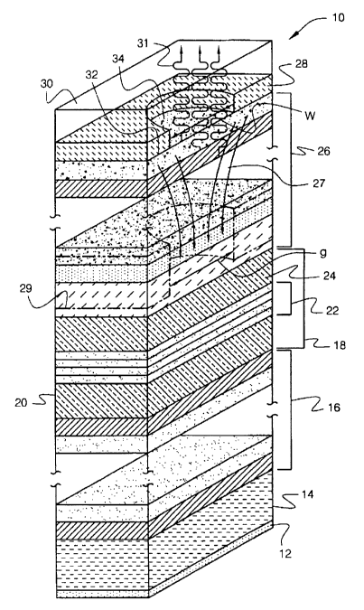
Figure 1 is a schematic illustration of a planar, current-guided, GaAs/AIGaAs
top
to surface emitting vertical cavity laser 10 in accordance with the prior art.
Formed on an
n-doped gallium arsenide (GaAs) substrate 14 is an n-contact 12. Substrate 14
is doped
with impurities of a first type (i.e., n type). An n-type mirror stack 16 is
formed on
substrate 14. Formed on stack 16 is a spacer 18. Spacer 18 has a bottom
confinement
layer 20 and a top confinement layer 24 surrounding active region 22. A p-type
mirror
stack 26 is formed on top confinement layer 24. A p-metal layer 28 is formed
on stack
26. The emission region may have a passivation layer 30.
Isolation region 29 restricts the area of the current flow 27 through the
active
region. Region 29 may be formed by deep H+ ion implantation. The diameter "g"
may
be set to provide the desired active area, and thus the gain aperture of the
VCSEL 10.
2o Further, the diameter "g" may be set by the desired resistance of the p-
type mirror stack
26, particularly through the non-conductive region 29. Thus, non-conductive
region 29
performs the gain guiding function. The diameter "g" is typically limited by
fabrication
limitations, such as lateral straggle during the implantation step.
Spacer 18 may contain a bulk or quantum-well active region disposed between
mirror stacks 16 and 26. Quantum-well active region 22 may have alternating
layers of
aluminum gallium arsenide (AIGaAs) barrier layers and GaAs quantum-well
layers.
InGaAs quantum wells may also be used in the active region, particularly where
an
emission wavelength (e.g. ~, = 980 nm) is desired where GaAs is transparent.
Stacks 16
and 26 are distributed Bragg reflector (DBR) stacks, and may include periodic
layers of
3o doped AIGaAs and aluminum arsenide (AIAs). The AIGaAs of stack 16 is doped
with
CA 02433357 2003-06-27
WO 02/059938 PCT/USO1/50214
9
the same type of impurity as substrate 14 (e.g., n type), and the AIGaAs of
stack 26 is
doped with the other kind of impurity (e.g., p type).
Metal contact layers 12 and 28 are ohmic contacts that allow appropriate
electrical biasing of laser diode 10. When laser diode 10 is forward biased
with a more
positive voltage on contact 28 than on contact 12, active region 22 emits
light 31 which
passes through stack 26.
Most VCSELs of practical dimensions are inherently multi (transverse) mode.
Single lowest-order mode VCSELs are favored for coupling into single-mode
fibers, and
are advantageous for free-space and/or wavelength sensitive systems, and may
even be
1o beneficial for use in extending the bandwidth-length product of standard 50
pm and 62.5
~m GRIN mufti-mode fiber. However, it has long been known that, although the
short
optical cavity (2 ~,) of the VCSEL favors single longitudinal mode emission,
the multi-
wavelength (10 ~,) lateral dimensions facilitate mufti-transverse mode
operation.
As indicated above, higher order modes typically have a greater lateral
concentration of energy away from the center of the optical or lasing cavity.
Thus, the
most obvious way to force the laser to oscillate in only a lowest order
circularly
symmetric mode is to make the lateral dimension "g" of the active area small
enough to
prevent higher-order modes from reaching threshold. However, this necessitates
lateral
dimensions of less than about 5 pm for typical VCSELs. Such small areas may
result in
2o excessive resistance, and push the limits obtainable from conventional
fabrication
methodologies. This is particularly true for implantation depths of greater
than about
1 pm, where lateral straggle may become a limiting factor. Thus, control of
transverse
modes remains difficult for VCSEL's of practical dimensions.
One illustrative approach for controlling transverse modes of an
optoelectronic
device is shown in Figure 2. Figure 2 is a schematic cross-sectional side view
of a planar,
current-guided, GaAslAlGaAs top surface emitting vertical cavity laser, as in
Figure l,
with a top mounted mode control resonant reflector 50. The resonant reflector
50
includes a patterned first material layer 56 that is positioned on top of the
top mirror layer
52 of VCSEL 54. A second material layer 58 is provided over the patterned
first material
layer 56, as shown.
CA 02433357 2003-06-27
WO 02/059938 PCT/USO1/50214
The first material layer 56 preferably has a refractive index that is greater
than the
refractive index of the second material layer 58, and the first and second
material layers
56 and 58 preferably have a refractive index that is less than the refractive
index of the
top mirror layer 52 of the optoelectronic device 54. In one example, the first
material
5 layer 56 is Si02, the second material layer 58 is Si3N4 or TiOz, and the top
mirror layer
52 is AIGaAs, although other suitable material systems are contemplated. Each
layer is
preferably an even multiple of one-quarter wavelength (~, /4) thick. This
causes a
reduction in reflectivity of the resonant reflector 50 in those regions that
correspond to
the etched regions 60 (see Figure 3B) in the first material layer 56, that is,
those regions
l0 that are filled with the second material layer 58. By designing the etched
regions to
circumscribe the desired optical cavity, this difference in reflectivity can
be used to help
provide mode control for VCSEL 54.
In forming the resonant reflector 50, and referring now to Figure 3A, the
first
material layer 56 is provided over the top minor layer 52. As shown in Figure
3B, the
first material layer 56 is patterned, preferably by etching away the first
material layer 56
in the region or regions circumscribing the desired optical cavity of the
VCSEL 54. As
shown in Figure 3C, a second material layer 58 is provided over the first
material layer
56. The second material layer 58 is preferably provided over both the etched
60 and non-
etched regions of the first material layer 56, but may be confined to the non-
etched
2o regions if desired. Selected regions, such as regions 62a and 62b o_f the
second material
layer 58 may then be removed to provide access to the top mirror layer 52.
Then, and as
shown in Figure 3D, a contact layer 64 may be provided on the exposed regions
of the
top mirror layer 52. The contact layer 64 may provide electrical contact to
the top mirror
layer 52.
In a related embodiment, a top mirror layer of the optoelectronic device may
function as the first material layer 56 discussed above. Thus, the top mirror
layer may
be patterned, preferably by etching at least partially into the top mirror
layer in the region
or regions circumscribing the desired optical cavity of the optoelectronic
device. In one
embodiment, the layer 52 below the top mirror layer may function as an etch
stop layer.
Then, a second material layer 58 is provided over the top mirror layer. The
second
CA 02433357 2003-06-27
WO 02/059938 PCT/USO1/50214
11
material layer is preferably provided over both the etched and non-etched
regions of the
top mirror layer, but may only be provided over the non-etched regions, if
desired. In this
embodiment, the regions labeled 56 in Figures 2-3 should have the same cross-
hatch
pattern as layer 53, and the refractive index of these regions should be less
than the
refractive index of layer 52.
Another illustrative approach for controlling transverse modes of an
optoelectronic device is shown in Figure 4. Figure 4 is a schematic cross-
sectional side
view of a planar, current-guided, GaAs/AIGaAs top surface emitting vertical
cavity laser,
as in Figure l, with another illustrative top mounted mode control resonant
reflector 70.
l0 In this embodiment, the resonant reflector 70 is formed by etching down
into but not all
the way through one or more of the top mirror layers 72 of the optoelectronic
device.
The etched region, generally shown at 74, preferably circumscribes the desired
optical
cavity of the optoelectronic device, and has a depth that causes a phase shift
that reduces
the reflectivity of the resonant reflector 70 at the desired operating
wavelength, such as
a depth that corresponds to an odd multiple of 7~,/4. To provide further
differentiation,
a cap mirror 76 having one or more additional layers may be provided on
selected' non-
patterned regions 78 °of the top mirror layer 72, such as over the
desired optical cavity of
the optoelectronic device. The cap mirror 70 may include one or more periods
of a
conventional semiconductor DBR mirror, or more preferably, a narrow band
dielectric
2o reflection filter. A metal layer may be provided on selected regions of the
top mirror
layer 72. The metal layer may function as a top contact layer.
In forming the resonant reflector 70, and refernng now to Figures SA-5B, a top
mirror layer 72 (or some other top layer) is patterned and etched to form one
or more
etched regions 74. The etched regions 74 are preferably formed to circumscribe
the
desired optical cavity of the optoelectronic device. Also, the etched regions
74 are
preferably etched down to a depth that causes a phase shift in the incident
light, thereby
reducing the reflectivity of the resonant reflector 70 in those regions.
Next, and as shown in Figure SC, a cap mirror 76 is formed on the patterned
top
mirror layer 72. As indicated above, the top mirror layer 72-may include one
or more
semiconductor DBR mirror periods, and/or a narrow band dielectric reflection
filter. In
CA 02433357 2003-06-27
WO 02/059938 PCT/USO1/50214
12
either case, and to provide further differentiation in reflectivity, the cap
mirror 76 may
be etched away except on those areas that correspond to the desired optical
cavity of the
optoelectronic device. This is shown in Figure SD. Alternatively, the
patterned cap
mirror 76 may be formed using well known lift-off techniques. Thereafter, a
contact
layer 80 may be provided on the selected regions of the top mirror layer 72.
The contact
layer 80 may provide electrical contact to the top mirror layer 72.
Another illustrative approach for controlling transverse modes of an
optoelectronic device is shown in Figure 6. Figure 6 is a schematic cross-
sectional side
view of a planar, current-guided, GaAs/AIGaAs top surface emitting vertical
cavity laser,
to as in Figure 1, with yet another illustrative top mounted mode control
resonant reflector
90. In this illustrative embodiment, the resonant reflector 90 has a
refractive index that
does not abruptly change across the optical cavity of the optoelectronic
device.
In a preferred embodiment, the resonant reflector 90 has at least one resonant
reflector layer 92 that has a refractive index. The refractive index may
include, for
example, contributions from both a first material 94 having a first refractive
index and
a second material 96 having a second refractive index. In a preferred
embodiment, the
first material 94 is confined to a first region and the second material is
confined to a
second region, wherein the first region and the second region co-extend along
an interface
98. By making the interface 98 non-parallel with the optical axis 100 of the
optoelectronic device, the refractive index of the resonant reflector layer,
at least when
viewed laterally along the optical cavity of the optoelectronic device, does
not change
abruptly across the optical cavity. Rather, there is a smooth transition from
one refractive
index to another. This reduces the diffraction effects caused by abrupt
changes in the
refraction index. It is contemplated that one or more periods of a
conventional
semiconductor DBR mirror, or more preferably, a narrow band dielectric
reflection filter
106, may be provided on top of the resonant reflector 90, as shown. Finally, a
contact
layer 102 may be provided around the periphery of the optical cavity. In the
embodiment
shown, the contact layer 102 is in direct contact with the top mirror layer
104 and
provides electrical contact to the top mirror layer 104.
3o The smooth transition from one refractive index to another is further
illustrated
CA 02433357 2003-06-27
WO 02/059938 PCT/USO1/50214
13
in chart 110. The X axis of chart 110 represents the lateral position along
the optical
cavity of the device shown above the chart. The Y axis of chart 110
corresponds to the
reflectivity "R" of the top mirror, including the resonant reflector 90 and
conventional
semiconductor DBR mirror or dielectric reflection filter 106. The reflectivity
"R" of the
top mirror, at least in the region of the resonant reflector 90, is dependent
on the
refractive index of the resonant reflector layer 90.
Traveling from left to right laterally along the optical cavity of the
optoelectronic
device, the reflectivity starts at a first value 112. The first value 112 is
shown relatively
low because the resonant reflector 90 and the conventional semiconductor DBR
mirror
or dielectric reflection filter 106 do not extend out into this region. The
contact layer 102
may also decrease the reflectivity in this region.
At the edge of the resonant reflector 90, the reflectivity increases to a
value 114,
which includes contributions from the second material 96 of the resonant
reflector layer
90 and the conventional semiconductor DBR mirror or dielectric reflection
filter 106.
Moving further to the right, the refractive index of the resonant reflector 90
begins to
change due to the relative contributions of the first material 94 and the
second material
96. This causes the reflectivity of the resonant reflector 90 to smoothly
increase toward
the center of the desired optical cavity, as shown. Preferably, the
reflectivity of the
resonant reflector 90 reaches a maximum 116 in or around the center of the
desired
optical cavity. The reflectivity of the resonant reflector 90 then decreases
to the right of
the center of the desired optical cavity, in an opposite manner to that
described above.
As can be seen, the refractive index, and thus the reflectivity, of the
resonant reflector
90 does not change abruptly across the optical cavity. Rather, there is a
smooth transition
from one refractive index to another. This reduces the diffraction effects
often caused by
abrupt changes in the refraction index of a resonant reflector.
Figures 7A-7D are schematic cross-sectional side views showing a first
illustrative method for making the resonant reflector of Figure 6. In this
illustrative
embodiment, a first substantially planar layer of material 94 is provided on,
for example,
a top mirror layer 104 of .a conventional DBR mirror. The top mirror layer 104
3o preferably has a refractive index that is higher than the refractive index
of the first layer
CA 02433357 2003-06-27
WO 02/059938 PCT/USO1/50214
14
of material 94. The top mirror layer 104 may be, for example, AIGaAs, and the
first layer
of material 94 may be, for example, Ti02, Si3N4, or a polymer such as
polyamide or
Benzocyclobuthene (BCB).
The first layer of material is then patterned, as shown in Figure 7A. This is
typically done using a conventional etch process. As shown in Figure 7B, the
patterned
first layer of material 104 is then heated, which causes it to reflow. This
results in a non
planar top surface 98. Then, and as shown in Figure 7C, a second layer of
material 96
is provided over the first layer of material 94. The top surface 105 of the
second layer
of material 96 is preferably substantially planar, but it may be non-planar if
desired. The
to second layer of material 96 preferably has a refractive index that is lower
than the
refractive index of the first layer of material 94. The second layer of
material 96 may be,
for example, Si02, a polymer, or any other suitable material. When desired,
the top
surface 105 of the second layer of material 96 may be planarized using any
suitable
method including, for example, reflowing the second layer of material 96,
mechanical,
chemical or chemical-mechanical polishing (CMP) the second layer of material
96, etc.
In some embodiments, the top surface 105 is left non-planar.
The second layer of material 96 is preferably provided over the entire top
surface
of the resonant reflector, and etched away in those regions where a top
contact 102 is
desired. Once the second layer of material 96 is etched, a contact layer 102
is provided
2o on the exposed regions of the top mirror layer 104. The contact layer 102
provides
electrical contact to the top mirror layer 104. As shown in Figure 7D, a cap
mirror 106
may then be provided above the second layer of material 96. The cap mirror 106
may
include one or more periods of a conventional semiconductor DBR mirror, or
more
preferably, a narrow band dielectric reflection filter.
Figures 8A-8E are schematic cross-sectional side views showing another
illustrative method for making the resonant reflector of Figure 6. In this
illustrative
embodiment, and as shown in Figure 8A, a first substantially planar layer of
material 94
is provided on, for example, a top mirror layer 104 of a conventional DBR
mirror. The
top mirror layer 104 preferably has a refractive index that is higher than the
refractive
index of the first layer of material 94. The top mirror layer 104 may be, for
example,
CA 02433357 2003-06-27
WO 02/059938 PCT/USO1/50214
AIGaAs, and the first layer of material 94 may be, for example, Ti02, Si3N4,
or any
other suitable material. Next, a photoresist layer 110 is provided and
patterned on the first
layer of material 94, preferably forming an island of photoresist above the
desired optical
cavity of the optoelectronic device.
5 As shown in Figure 8B, the photoresist layer 110 is then heated, causing it
to
reflow. This results in a non-planar top surface on the photoresist layer 110.
That is, the
top surface of the photoresist layer 110 may have portions that taper down
toward the
first layer of material 94. Next, and as shown in Figure 8C, the photoresist
layer 110 and
the first layer of material 94 are etched for a specified period of time. The
etchant
to preferably selectively etches both the photoresist layer 110 and the first
layer of material
94. This transfers the shape of the non-planar top surface of the photoresist
layer 110 to
the first layer of material 94.
As shown in Figure 8D, a second layer of material 96 is then provided over the
first layer of material 94. The second layer of material 96 preferably has a
refractive
i5 index that is less than the refractive index of the first layer of material
94. The second
layer of material 96 is preferably provided over the entire top surface of the
resonant
reflector, and etched away in those regions where a top contact 102 is
desired. Once the
second layer of material 96 is etched, a contact layer 102 is provided on the
exposed
regions of the top mirror layer 104. The contact layer 102 provides electrical
contact to
-the top mirror layer 104. Preferably, the top surface of the second layer of
material 96
is substantially planar. As shown in Figure 8E, a cap mirror 106 may be
provided above
the second layer of material 96, if desired. The cap mirror 106 may include
one or more
periods of a conventional semiconductor DBR mirror, or more preferably, a
narrow band
dielectric reflection filter.
Figures 9A-9E are schematic cross-sectional side views showing yet another
illustrative method for making the resonant reflector of Figure 6. In this
illustrative
embodiment, and as shown in Figure 9A, a first substantially planar layer of
material 94
is provided on, for example, a top mirror layer 104 of a conventional DBR
mirror. Like
above, the top mirror layer 104 preferably has a refractive index that is
higher than the
refractive index of the first layer of material 94.
CA 02433357 2003-06-27
WO 02/059938 PCT/USO1/50214
16
Next, and as shown in Figure 9B, the first layer of material 94 is patterned,
preferably forming an island above the desired optical cavity of the
optoelectronic device.
This results in the first layer of material 94 having lateral surfaces 118
that extend up to
a top surface 116 that is defined by top peripheral edges 120. A photoresist
layer 114 is
then provided over the patterned first layer of material 94, including over
the lateral
surfaces 118, the top peripheral edges 120 and the top surface 116. Because of
the step
between the top surface 116 and the lateral surfaces 118, the photoresist
layer 114 is
thinner near the top peripheral edges 120 than along either the lateral
surfaces 118 or top
surface 116 of the patterned first layer of material 94, as shown.
1o As shown in Figure 9C, the photoresist layer 114 and the first layer of
material
94 are then etched for a specified period of time. During this etch step,
those regions of
the first layer of material 94 that are adjacent the thinner regions of the
photoresist layer
114 are subject to the etchant for a longer period of time than those regions
that are
adjacent thicker regions of the photoresist layer 114. Thus, and as shown in
Figure 9C,
the top peripheral edges 120 of the first layer of material 94 are etched more
than those
regions away from the top peripheral edges 120, resulting in tapered edges
122.
After the etching step, and as shown in Figure 9D, a second layer of material
96
may be provided over the first layer of material 94. Like above, the second
layer of
material 96 preferably has a refractive index that is less than the refractive
index of the
first layer of material 94. The second layer of material 96 is preferably
provided over the
entire top surface of the resonant reflector, and etched away in those regions
where a top
contact 102 is desired. Once the second layer of material 96 is etched, a
contact layer 102
is provided on the exposed regions of the top mirror layer 104. The contact
layer 102
provides electrical contact to the top mirror layer 104. Preferably, the top
surface of the
second layer of material 96 is substantially planar.
As shown in Figure 9E, a cap mirror 106 may be provided above the second layer
of material 96, if desired. The cap mirror 106 may include one or more periods
of a
conventional semiconductor DBR mirror, or more preferably, a narrow band
dielectric
reflection filter.
3o Figure 10 is a schematic cross-sectional side view showing another
illustrative
CA 02433357 2003-06-27
WO 02/059938 PCT/USO1/50214
17
embodiment of the present invention similar to that shown in Figures SA-SD. In
this
embodiment, a top layer 110, which may be the top mirror layer of the top DBR
mirror
stack of the optoelectronic device or an additional layer on top of the top
mirror layer,
may be etched down - but not all the way through. The etched region preferably
circumscribes the desired optical cavity of the optoelectronic device, and has
a depth that
causes a phase shift that reduces the reflectivity of the resonant reflector
at the desired
operating wavelength, such as a depth that corresponds to an odd multiple of
7J4. Like
in Figures SA-SD, a cap mirror 112 having one or more additional layers may be
provided on selected non-patterned regions of layer 110, such as over the
desired optical
to cavity of the optoelectronic device, to provide further differentiation in
reflectivity. A
metal layer 114 may then be provided on the etched region of layer 110. The
metal layer
may function as the top contact. By extending the metal layer 114 all the way
or near the
cap mirror 112, better current spreading can be achieved for the
optoelectronic device.
Figure 11 is a schematic cross-sectional side view showing another
illustrative
embodiment of the present invention similar to that shown in Figures SA-SD.
This
embodiment is similar to that of Figure 10, but the metal layer, now labeled
116, extends
over the etched region of layer 110 and over the cap mirror 112. For back
illumination
devices, this may provide even better current spreading for the optoelectronic
device.
Figure 12 is a schematic cross-sectional side view showing another
illustrative
-embodiment of the present invention similar to that shown in Figures 8A-8E. A
resonant
reflector is provided that has a refractive index that does not change
abruptly across the
optical cavity of the optoelectronic device. The illustrative resonant
reflector includes
at least one resonant reflector layer that has a refractive index that
includes contributions
from, for example, both a first material 120 having a first refractive index
and a second
material 122 having a second refractive index. In the embodiment shown, the
first
material 120 is confined to a first region and the second material 122 is
confined to a
second region, wherein the first region and the second region co-extend along
an
interface. A metal layer 124 is then provided over the entire structure. For
back
illumination devices, the metal layer 124 may provide enhanced current
spreading when
3o compared to the device shown in Figures 8A-8E.
CA 02433357 2003-06-27
WO 02/059938 PCT/USO1/50214
18
Having thus described the preferred embodiments of the present invention,
those
of skill in the art will readily appreciate that the teachings found herein
may be applied
to yet other embodiments within the scope of the claims hereto attached.