Note: Descriptions are shown in the official language in which they were submitted.
CA 02433391 2005-09-15
COMMUNICATION SYSTEM FOR MOBILE USERS
USING ADAPTIVE ANTENNA
Technical Field
[0001] The present invention relates generally to a communication system and
more particularly, to a communication system using a ground-based base station
and a
gateway station that performs beam control at the gateway station.
Background Art
[0002] In this communication age, content providers are increasingly
investigating ways in which to provide more content to users as well as
interfacing
with users.
[0003] The Internet has increased the need for consumer information at high
speeds. DSL and cable modems are increasing in popularity because they provide
higher byte rates than telephone and modem-based systems. Providing broadband
access through cable or DSL service requires increased infrastructure. That
is, cables
must be laid through which service is provided. Cables are time consuming and
costly to provide as well as costly to maintain.
(0004] Because of high competition, cost for providing service is an important
factor. Also, providing high data rates is also an important factor.
[0005] Limitations to the number of users may be inhibited by interference in
systems. For example, for every beam having a main lobe, a parasitic number of
side
lobes exist which may cause interference with beams using the same system
resource
such as frequency.
[0006] It would therefore be desirable to provide a mobile communication
system that is capable of rapid deployment, is easy to change, should the
technology
inevitably change and reduces the amount of interference with adjacent beams
to
permit high throughput.
CA 02433391 2005-09-15
2
Summary of the Invention
[0007] The present invention provides a communication system that allows
rapid deployment and provides interference rejection. The present invention is
suitable for both fixed users such as those positioned in a building or home
or for
mobile users.
[0008] According to an aspect of the present invention, there is provided a
communications system comprising: a base station having an adaptive antenna
with a
plurality of panels, each panel having a plurality of main array antenna
elements for
simultaneously generating a plurality of dynamic communication beams; and a
gateway station coupled to said base station, said gateway station forming a
plurality
of beams commands for each of the plurality of panels by communicating a
plurality
of control signals to the base station to form the communication beams.
[0009] According to another aspect of the present invention, there is provided
a
method of operating a communication system having a gateway station and a
plurality
of base stations comprising: at the gateway station, dividing a communication
signal
into a control signal corresponding to a plurality of elements of a plurality
of panels of
a plurality of adaptive antennas of the plurality of base stations, said
control signals
corresponding to a plurality of multiple dynamic links directing the control
signals to
the plurality of base stations; and
generating the multiple dynamic links from the plurality of panels of
the, plurality of base stations so that more than one dynamic link is
generated
simultaneously from one panel.
[0010] One advantage of the invention is that due to the interference
detection,
system throughput is increased over conventional systems.
[0011) Another advantage of the invention is that by locating a majority of
the
processing remote from the base stations, overall costs of systems may be
further
reduced.
CA 02433391 2003-06-27
WO 02/058186 PCT/US02/00842
3
[0013] Other features and advantages of the present invention using remote
digital
beam forming are readily apparent from the following detailed description of
the best mode
for carrying out the invention when taken in connection with the accompanying
drawings.
Brief Description of the Drawings
[0014] Figure 1 is a system diagram of a communication system according to the
present invention.
[0015] Figure 2A is a top view of a base station antenna according to the
present
invention.
(0016] Figure 2B is aside view of the base station antenna of Figure 2A.
(0017] Figure 2C is a side view of a panel of the base station of Figure 2A
illustrating
elements thereon.
(0018] Figure 2D is an alternative side view showing elements of a panel of a
base
station.
(0019] Figure 2E is a third alternative embodiment of elements of a panel of
an
antenna according to the present invention.
[0020] Figure 3 is a high level block diagrammatic view of element modules
coupled
to a data bus.
(0021] Figure 4 is a beam pattern~for the panel illustrated in Figure 2.
[0022] Figure 5 is a block diagrammatic view of a digital beam forming circuit
according to the present invention.
(0023] Figure 6 is a block diagrammatic view of a beam forming circuit using
noise
injection according to the present invention.
CA 02433391 2003-06-27
WO 02/058186 PCT/US02/00842
4
(0024] Figure 7 is a block diagrammatic view of a base station pxocessing
circuit
according to the present invention.
(0025] Figure 8 is a block diagrammatic view of a gateway processing station
according to the present invention.
(0026] Figure 9 is a more detailed schematic view of a demultiplexing beam
forming
and nulling circuit according to the present invention.
(0027] Figure 10 is an alternative for the remote processor; an adaptive
digital beam
forming and nulling processor according to the present invention.
(0028] Figure 11 is an alternative nulling circuit with a limiter on the
feedback path
according to the present invention.
(0029] Figure 12A is an output of a digital beam forming circuit not including
limiter
as shown in Figure 10.
(0030] Figure 12B is an output of the circuit of Figure 10 with limiters at
all feed-
through paths.
(0031] . Figure 12C is an output of circuit shown in Figure 11 with limiter on
the feed-
back path, wherein the power density levels of both the weak and strong
interference is
successfully reduced below a threshold.
(0032] Figure 13 is an alternative digital beam forming and nulling processor
using
auxiliary elements.
Best Modes For Carrying Out The Invention
(0033] In the following description, the same reference numerals are used to
identify
the same components in the various views. Those skilled in the art will
recognize that
various other embodiments, structural changes and changes in measures may be
made
CA 02433391 2003-06-27
WO 02/058186 PCT/US02/00842
without departing from the scope of the invention. The teachings of the
present invention
may be used for both fixed users as well as mobile users.
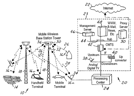
[0034] Referring now to Figure l, a communications system 10 has a plurality
of
beams 12 that are illustrated as a plurality of circles 14 on the earth's
surface. Circles 14
represent the footprint of a radiated beam onto the earth's surface. A
plurality of user
terminals 16M and 16F are used to illustrate mobile users and fixed users,
respectively.
Mobile users 16M may comprise but are not limited to automotive applications,
personal
digital assistant applications and cellular phone applications. Fined user
terminals 16F may,
for example, comprise business-based or consumer-based communication systems.
Each user
terminal 16F and 16M may receive a signal with the predetermined signal
strength from a
communication beam or communication beams through multiple links from one or
more base
stations 18. The present invention is particularly advantageous for use with
mobile terminals
16M. Although only two wireless basestations are illustrated, they may each
represent a
plurality of basestations.
[0035] Communication system 10 further includes a gateway station 20 that is
coupled to terrestrial networks 22. Gateway station 20 may be coupled to a
base station
processing center 24. Gateway station 20 provides a links between user
terminals 16F, 16M
and terrestrial networks 22 through base stations 18. Gateway station 20 may
be coupled to
terrestrial networks 22 such as the public service telephone network, the
Internet, or an
intranet. Although illustrated as two separate units, gateway station 20 and
processing center
24 may be combined into the same physical location.
[0036] The communication signals between base station 18 and user terminals
16M
and 16F may be referred to as user links 26. User links 26 represent the
transmit and receive
beams from both categories of user terminals 16F, 16M and base station 18. A
feeder link 28
is defined between base station 18 and gateway station 20.
[0037] Base stations 18 are used as a communication nodes for gateway station
20
and user terminals 16F and 16M. For communicating with user terminals 16M and
16F, base
CA 02433391 2003-06-27
WO 02/058186 PCT/US02/00842
6
stations 18 have an adaptive antenna 30 formed of panels of reconfigurable
elements as will
be further described below. Each base station 30 also has a directional
antenna 32 for
coupling to gateway station antenna 34. The coupling of antennas 32 and 34
allows base
station 18 to be wireless and therefore advantageously be easily deployed. As
will be
described below, the pointing from both mobile terminals 16M and base station
18 may be
performed electronically. Although only one gateway station 20 is illustrated
in the figure,
those skilled in the art would recognize that various numbers of gateway
stations may be
employed. Gateway station 20 has a gateway control circuit 23 that controls
the content and
communication with the base station 18.
(0038] Base station 18 has a controller 36 that links user terminals 16M, 16F
through
antenna 32 with gateway station 20. In the present example, the controller 36
is used in the
return link direction to multilplex received signals from all the array
element into the feeder
link signals 28 as determined in the gateway station 20. Similarly in the
forward link
direction, controller 36 is used to de-multiplex the feeder link signals into
various streams of
signals for array elements to transmit.
(0039 Gateway control circuit 23 may have various circuitry coupled thereto.
For
example, analog or digital TV 38, an up converter 40, and a cable modem
terminal shelf
(CMTS) 42. CMTS 42 may be used to couple to terrestrial networks such as
Internet 22.
CMTS 42 may be coupled to a hub 44 that has various resources coupled thereto.
The hub 44
may, for example, have a management server 46, a world wide web, e-mail or
news server 48
or a proxy server S0.
(0040 Referring now to Figures 2A, 2B, 2C, and 2D, antenna 30 is shown in
further
detail. In the illustrated embodiment, antenna 30 has five panels 52 that are
used to direct
communication signals to a desired direction. As is illustrated best in Figure
2A, each panel
52 has a field of view and a scanning range slightly narrower than the field
of view. Each
panel is preferably a flat panel that allows cost effective multiple
connectivity from base
station 18 to the various users. Each panel 52 is used to establish multiple
dynamic links. In
combination, the various base stations together are used to form the
communication signal
CA 02433391 2003-06-27
WO 02/058186 PCT/US02/00842
7
with the users. Thus, multiple base stations through multiple panels 52 of
antennas 30 are
used in each communication. The bandwidth on demand is accomplished not by a
variety of
data rates via a single rf link but through different data rates resulting
from various
combinations of multiple dynamic rf links. As will be further described below,
as the user
moves, some links may fade away while new links may become available. Thus,
multiple
links will always be connected to a user. As illustrated, five panels are
used, however, those
skilled in the art will recognize various numbers of panels may be used.
(0041 As is best shown in Figure 2B, panels 52 have an angle 54 relative to
the
horizontal. Angle 54 allows the communication signals generated at panels 54
to be directed
slightly downward toward the earth's surface. Of course, angle 54 depends on
the height of
base station 18 above the earth's surface. That is, as the height of the tower
increases, the
angle 54 decreases. The angle is such to give a desired service area for each
panel 52.
(0042 In operation, the combination of simultaneous multiple beam capability
on
both the mobile terminals and base stations will make overall mobile systems
even more cost
effective. A user through their associated multiple beam user device or
appliance will
connect to an IP network by establishing multiple dynamic links through
various base
stations to the communication nodes of the Internet. As a result, precious
mobile spectrum
may be reused many times when mobile subscribers use directional antennas. The
same
amount of spectrum can be used again and again to increase the bandwidth
density (i.e., total
bandwidth a mobile system can project into a unit area). Therefore, the system
will provide
more throughput for users and larger capacity for the operators, and more
efficient utilization
for regulators. Providing a high gain on both user terminals and base stations
allows the cell
size to be extended extensively without impacting the bandwidth density. The
bandwidth on
demand will be implemented through multiple dynamic links and thus multiple
links will
always be available to a user. There may be many bases stations within a held
of view of a
mobile user. For example, there may be as many as between five and ten bases
stations
within a user's field of view. A user with an omni directional terminal may
connect to one
nearest base station with an rf channel (specified by frequency, time and/or
code). This
channel will not be assigned to other users as in a conventional cellular
system. Adaptive
CA 02433391 2003-06-27
WO 02/058186 PCT/US02/00842
8
antennas on base stations allow operators to use the same channel again within
the same
"cell" but via different base stations, provided the base stations have the
capability to
directionally discriminate against interferences at the same channel as that
intended user but
at different directions. As will be further described below, the user and
interference sources
must be located reasonably far to make the adaptive technique effective. The
base stations
may include circuitry to null or offset interferences between the
communication signals.
During an acquisition phase, e.g., from a cold start, all received beams will
be "on" to cover
the entire field of view of a fan beam. Thus, the various beams will have
different elevation
angles and azimuth angles to cover the search volume. Once a user link is
established, only
nearby beams from a particular panel 52 may be activated.
[0043 Once a user link is established, the tracking mechanism uses a type of
step
scan principle. The signal strengths from adjacent received beams will be
monitored and
compared with one coming from the main beam. The beam with the strongest
signal will be
identified as a "locked" or main beam. As a user moves, the tracking base
station may switch
(i.e., step) a received beam from one position to an adjacent one with the
strongest signal, and
assign the transmit beam accordingly.
[0044 As is best shown in Figure 2C, a panel 52 may be comprised of a
plurality of
radiation elements or patches 56. Radiation elements 56 may, for example, be
described as a
"patch array." As is illustrated, 90 elements are illustrated in Figure 2C.
Each element 56
has a diameter of 0.3 wavelengths. Element modules are placed at slightly less
than 0.7
wavelengths apart in a nearly square lattice. Panel 52 may also be xeferred to
as an
"aperture." Panel 52 has a radiating area in the order of about 25 square
wavelengths. The
expected peak gain of a beam is 24dB at the boresight, and about 22dB at 45
degrees away
from the boresight. Beam widths for the boresight elliptical beam is about 10
degrees in
azimuth and 15 degrees in elevation respectively. The beams are dynamic and
therefore
assigned to track individual subscribers accordingly.
CA 02433391 2003-06-27
WO 02/058186 PCT/US02/00842
9
(0045] Referring now to Figure 2D, a 45 element panel 52 is illustrated. Such
a panel
has about 3dB less gain than that of the panel illustrated in Figure 2C while
maintaining
about the same directional discrimination.
(0046] Referring now to Figure 2E, another element configuration of a flat
panel 52 is
illustrated for a high frequency application. In this embodiment, panel 52 has
about 36
elements. In this embodiment, each element is approximately 0.6 wavelengths in
diameter
with element spacing slightly less than 0.7 wavelengths apart in a nearly
square lattice. The
total aperture has a rating area in the order of about 10 square wavelengths.
The peak
expected gain of the beam is about 20dB at boresight and lBdB 45 degrees away
from the
boresight. The beam widths for the boresight elliptical beam are about 5
degrees in azimuth
and 15 degrees in elevation, respectively. Therefore, at 2 kilometers away
from the base
station, the beam width and azimuthal direction is about 200 meters. Of
course, fewer
elements may be used depending on the frequencies involved. That is for higher
frequencies
because more data is transferred, less elements may be required to match the
processing
power of the circuitry.
(0047] For each of the above embodiments, long baselines, not full apertures,
over a
large bandwidth provide good directional discrimination capability. The thin
array at a single
frequency will exhibit high side lobes or semi-grading lobes. Over a large
bandwidth, side
lobes arise at various directions at different frequency components. As a
result, the integrated
interference contribution from side lobes over a large bandwidth tends to
smear out or cancel
while the contribution to the main lobe over the same bandwidth maybe
constructively added
together. As will be further described below, additional cancellation schemes
may be applied
to reject interferences for all beams tracking to various subscribers if
necessary.
(0048] Referring now additionally to Figure 3, radiating elements 56 form
modules
58 which are plugged into panels 52. Panels 52 serve as back plates which are
interconnected
through a bus 60. Bus 60, for example, may include a DC power line 62, an
inflow data line
63, an outflow data line 64, an address line 65, and a control line 66. Panels
52 may be
modularized and include sockets for easy connection and disconnection of
modules 58. Each
CA 02433391 2003-06-27
WO 02/058186 PCT/US02/00842
panel or back plate 52 may include a processor 68 to handle beam
configuration. Processor
68 may be part of controller 36 described above in Figure 1.
[0049] Referring now to Figures 2E and 4, a beam pattern 69 for the panel of
Figure
2E is illustrated. The pattern 69 has circles 70 or ellipses representing beam
positioning
patterns from a dynamic beam allocation and positioning scheme, while the
hexagon 71
representing fixed beam positions from a conventional static cell system.
Panel 52 converts
th.e received microwave power into a digital stream in the receiving direction
and converts the
digital stream into radiated microwave power in the transmitting direction.
The phasing of
various elements is implemented by digital multiplication in a separated
digital beam former.
The digital beam forming approach eliminates the need of conventional phase
shifters and
minimizes required rf components, making possible a low cost implementation
suitable for
the consumer market.
(0050] Referring now to Figure 5, a digital beam forming circuit 72 is
illustrated for a
base station (of Figure 1). However, a similar beam forming circuit may also
be used for a
user device. Also, a receive beam forming network is shown, however, those
skilled in the
art will recognize a corresponding transmitting beam forming circuit may be
formed in
reverse.
(0051] Digital beam forming circuit 72 has a plurality of elements 74. Various
groupings of elements 74 are used to generate the simultaneous multiple links
of the present
invention. Each element 74 is coupled to a corresponding analog-to-digital
converter. As
those skilled in the art will recognize, a band pass filter (not shown) rnay
also be coupled
between element 74 and analog-to-digital converter 76. The digital outputs
from all of the
analog-to-digital converters 76 are weighted and summed, then grouped together
to form
beams 1 through M as illustrated. The beams are formed by numerical
multiplications using
the direction vector beam 1 as illustrated as reference numeral 78 and through
direction
vector beam M as illustrated by reference numerals 80 through forming circuit
82. Forming
circuit 82 may have a plurality of multiplication blocks 84 and summing blocks
86 either
implemented physically or in software to form the various beams. Functions of
beam
CA 02433391 2003-06-27
WO 02/058186 PCT/US02/00842
11
forming, frequency tuning and time synchronization are interlaced to minimize
the over
processing mode, instead of sequentially. This approach eliminates
conventional phase
shifters and minimizes the required rf components making the implementation
suitable for
consumer applications. Digital beam forming circuit 72 is used to generate
multiple
simultaneous links with base station 18. The digital beam forming circuit 72
is configured
such that a unique beam is assigned for each individual user. The base
stations will track
users with unique channels and beam positions. Every user will have a bubble
which is the
beam size associated with the assigned beam. The bubble forms an exclusion
zone associated
with each user for a specific channel. Users assigned with the same channel
can co-exist in a
network as long as their associated bubbles do not intercept one another. When
bubbles for a
particular channel collide, one user is assigned a new channel.
[0052 Direct samplings are used to simplify the architecture. Low cost is
achieved
by the use of an analog-to-digital converter 76 that allows analog-to-digital
conversion of the
received signals at rf directly allowing other processing to be performed
'digitally. High
speed and low speed analog-to-digital conversion will ~ over sample the
received signals. In
one constructed embodiment, a user signal is assumed to be about SMHz but
could go as high
as 30MHz. A sampling rate was chosen to be about 20MBps per second with
approximately
a 4-bit resolution. Aperture time of the analog-to-digital converter must less
than one-eighth
of the period of the Garner frequency. Therefore, at a 2GHz carrier frequency,
the aperture
time of about 50 picoseconds is adequate.
[0053 Referring now to Figure 6, an alternative to the circuit configuration
of Figure
is illustrated. In this embodiment, the number of analog-to=digital converters
is reduced
and the dynamic range required for the individual analog-to-digital converters
is also
reduced. In the circuit of Figure 6, element 74 may be weighted in block 88
before a summer
90. Summer 90 is used to group a number of elements together. Each summing
block 90 has
an analog-to-digital converter 92 associated therewith. Thus, by grouping a
number of
elements together with a summing block 90, the number of analog-to-digital
converters is
thus reduced. Each summing block 90 may also be connected to a noise injection
circuit 94.
Structured noise may be added to the summing block 90. The structured noise
may consist of
CA 02433391 2005-09-15
12
orthogonal codes. A similar technique is described in U.S. Patent No.
5,077,562.
(0054) Each analog-to-digital converter 92 is coupled to demultiplexer 96.
Demultiplexer 96 is coupled to digital beam forming and interference rejection
network 98. Demultiplexer 96 demultiplexes the outputs from analog-to-digital
converters 92 and provides them to digital beam forriiing and interference
rejection
network 98, Digital beam forming and interference rejection network provides a
received signal to be processed by the processing center.
[0055] Referring now to Figure 7, a similar embodiment to that shown in
Figure 6 above is illustrated. In this embodiment, a portion of the circuit
may be
located in base station while the remaining portion of the circuit may be
located in a
processing center. By removing some of the circuitry from a base station, a
less
costly and more flexible system may be obtained. The same reference numerals
are
used for the same elements in Figure 7 as in Figure 6. Elements 74 are coupled
to
weighted block 88 which in turn are coupled to summers 98. A weighted block
100 is
used after summer to couple summer 90 with a central summing block 102. The
signal from summing block 102 is thus broadcast or transmitted to the gateway
station
for further processing.
[0056] Referring now to Figure 8, a gateway portion 104 of the circuit
illustrated in Figure 7 is illustrated. A demultiplexer 96 similar to that
illustrated
above is used. Demultiplexer 96 demultiplexes the broadcast signal from summer
102 and provides it to an analog-to-digital converter 106. Analog-to-digital
converter
106 may be coupled to noise injection circuit 108. Noise injection circuit 108
may be
similar to that described above in that noise injection circuit 108 may use
orthogonal
codes. The output of analog-to-digital converter is provided to a
demultiplexer
portion 108 which in turn is coupled to digital beam forming and interference
rejection network 98 similar to that in Figure 6. Thus, digital beam forming
network
and digital interference rejection network provides received signals from the
various
beams. By providing the demulHplexing analog-to-digital conversion and noise
injection all in one location such as the gateway station, the complexity of
the base
stations
CA 02433391 2003-06-27
WO 02/058186 PCT/US02/00842
13
may be reduced. Further, the number of elements provided at a base station may
be increased
due to the remote processing of the beam signal.
[0057] Refernng now to Figure 9, a more detailed processing scheme for a CDMA
system, such as 3'd generation mobile, from that shown in Figures 8 is
illustrated. In this
embodiment, a diplexer 110 is connected to a radiator (not shown) so that both
transmit and
receive signals are through the same radiator. Only the receive functions are
illustrated. The
corresponding transmit functions are identical but in a reversed direction.
The received
multiplexed signals are coupled to an analog-to-digital converter 112. To
simplify the block
diagram, we did not include the noise injection portion in here. Following
analog-to-digital
converter 112 a element code despreading circuit 114 has a plurality of
multiplication blocks
116 which performs the matched filter function via a multiplication 116 and a
band pass alter
118, to recover the signal received at a specific array element in digital
representation.
Therefore at the outputs of the de-spreading block 114, the received signals
of all the array
elements at the remote base stations have been re-generated in digital forms.
The regenerated
signals are available for further processing.
[0058] A scheme in which every user will have a dedicated beam is illustrated.
The
received element signals by user codes are sorted element by element before
beam forming.
More than one user per code is used but they come from different directions
and arnving at
different time.
[0059] Element code despreading circuit 114 is coupled to a user code
despreading
circuit 120. Each user code is used to group multiple users with the same user
code together
in user code despreading circuit 120. Different users may only be separated
via time delay
and direction of arrival. Thus the block 120 must provide digital streams with
multiple taps to
beam forming network so that the user signals with the same user code can be
separated via
time and directional "filtering processes." Each user code from user code
despreading circuit
120 is coupled to digital beam and null forming network. One digital beam and
null forming
network is provided for each user. Track files 124 provide input to digital
beam forming and
null forming network 122. Track files include information such as the user
code, the
CA 02433391 2003-06-27
WO 02/058186 PCT/US02/00842
14
location, timing and orientation of the users. Track ales allow the
communication signals to
be divided into several links for communication through a number of base
stations. The user
signals after digital beam forming are output and coupled to such things as
the Internet.
Feedback is provided from output 126 through an extended Kalinan filter. The
extended
Kalman filter 128 is used to update each user position channel and potential
for interference
or collision with neighbors. The information from the extended Kalman filter
128 will be
used to track the corresponding user.
[0060] Referring now to Figure 10, an adaptive nulling circuit 130 that could
be used
with any of the circuits in Figures 7 through 9 is illustrated. For example,
the circuit 142 of
Figure 10 may be implemented as a part of element 122 of Figure 9. Circuit 130
has
elements 132 which are coupled to a beam forming circuit 134 and an analog-to-
digital
converter 136. Of course, as mentioned above, this portion of the circuit may
be similar to
that shown in Figures 7 through 9. A multiplication block 138 and amplifier
140 may also be
included in the circuit. A digital beam forming and nulling processor 142 is
coupled to each
analog-to-digital converter. Each signal is multiplied by a weight at
multiplication block 144
prior to being summed at a summer 146. The output of summer 146 is the output
signal Y~t~.
In a typical digital beam forming, the directional vector (the multiplier set)
is pre-determined
by pointing direction only, and usually will exhibit a linear phase
progression'on the array
apertures for spot beams . However, in the adaptive beam forming and nulling
network
illustrated, the directional vector will be further modulated by signal
environment, such that a
beam is directed toward desired user while nulls are steered toward high
interference
directions. As a result the received signal to noise (including interference)
ratio is
"maximized." Negative feedback block 147 is provided from output signal Y(~~
to a
multiplication block 148 for each signal. °The multiplication block 148
multiplies the input
signal from each analog-to-digital converter with the output signal Y~t~. A
sum through
summer block 150 is provided to a weight update block 152. Weight update block
152, thus
in response to the multiplication block 148, updates the weights and provides
those to
multiplication blocks 144. The output is thus,
CA 02433391 2005-09-15
Y(t) = EtWy Sr (t)
- C~~wB
dt r
(o~~), =2ty(t)-d (t)*s~ (t?~
[0061] Our method for adaptive pulling to use a least mean square criteria for
steady state solution. In' addition, a steepest descent technique may be used
to reach
the steady state solution. An indirect correlation technique is used, rather
than a direct
perturbation technique, to measure the "gradients" for each update.
[0062] Referring now to Figure 11, to reduce cost and enhance the pulling
efficiency, a limiter may be placed in the feedback path similar to the
techniques
described in U.S. Patent No. 4,635,063. Limiting circuit 160 includes elements
162
similar to those described above. Each element has an associated main channel
164, a
feedthrough path 166, and a feedback path 168. Since the circuitry associated
with
the respective elements are essentially the same, the circuitry associated
with only one
sensor is referenced in detail. The function blocks can all implemented in
digital
format. For Instance, power dividers correspond to data bus, weight circuits
to
multipliers, correlators to processors combining multipliers and integration-&-
dumps,
outputs of hard limiters to sign bits, and so on.
[0063] Correlators 170 co-process signals in the feedthrough path 166 and
feedback path 168; the result is transformed according to an algorithm by a
computer
172. The weighting circuit 174 thus progressively modifies the signal in the
main
channel 164 to minimize interference with a desired signal.
j0064] A limiter 176 is placed along feedback path 168. As explained below,
this placement simplifies correlator design relative to the circuit without
such limiters
and improves performance relative to adaptive antennas with limiters in the
feedthrough path. ,
(0065] Each element 162 is connected via the respective main channel 164 to
respective input power divider 180 or other means for dividing an input signal
between a pre-
CA 02433391 2003-06-27
WO 02/058186 PCT/US02/00842
16
processed signal and a diagnostic signal. A diagnostic signal is conveyed
along the
respective feedthrough path 166; the pre-process signal is conveyed along a
second portion
182 of the respective main channel 164.
[0066 The amplitude and phase of pre-process signals may be modified by
weighting
circuit 174 or other weighting means associated with each of the elements 162.
The resulting
weighted signals are directed along a third portion 184 of respective main
channel 164 to be
summed by means such as a power combiner 186. Means such as an output power
divider
188 inserted along a unified portion 190 of main channel 14 between the power
combiner 186
and antenna output 192, divides the summed signal between an output signal and
a feedback
signal.
[0067 The illustrated feedback path 168 includes means for eliminating from
the
feedback signal the desired band of frequencies associated with the primary
signal source to
be received by circuit 160. This means may include a hybrid 194 for
subtracting the desired
band from a portion of the summed signal. More particularly, hybrid 194
includes a primary
input 196 and a secondary input 198. The primary input 196 receives a portion
of the
summed signal from output power divider 188. The secondary input 198 receives
only the
part of the summed input with the desired band. The desired band may be
provided by means
of a band pass filter 200, the input of which is a portion of the summed
signal directed thereto
by output power divider 188. The output of hybrid is the summed signal less
the desired
band. The elimination of the desired band from the feedback signal avoids
possible nulling
against the desired signal source. The limiter 176 is located in feedback path
168 so that
limiting occurs prior to division of the feedback signal. Thus, the need for
plural Iimiters is
obviated. Preferably, limiter 176 is a hard limner. Ideally, a hard limiter
transforms a
sinusoidal input to a square wave output.
[0068 The limited feedback signal is divided by means such as power divider
202 to
provide feedback signals to provide feedback inputs 204 of correlators 170.
The feedback
signal is correlated with the diagnostic signal received at feedthrough input
206 of each
correlator 170: The preferred correlator 170 is a multiplier coupled with a
low pass alter.
CA 02433391 2003-06-27
WO 02/058186 PCT/US02/00842
17
[0069 Each correlation resultant is transformed according to an algorithm by
computer or processor 172 or alternative means. The transform is used to
determine the
weighting function of the weighting circuit 174 or other weighting means.
Preferably a
gradient descent algorithm such as least means square error, Howell-Applebaum
power
inversion, is used.
[0070 Some of the advantages of the present invention can be better understood
in
accordance with the following theoretical analysis. The function of the ideal
hard limiter is to
produce a high constant level positive output whenever the input is positive
and a low
constant level negative output whenever the input is negative. The transition
between the
constant positive and negative output values (or the threshold values) is a
sharp or
discontinuous one. Therefore, with a sinusoidal input the output would ideally
be a square
wave. In a multiple signal environment where the signal power differences are
large (e.g.,
more than 10 dB), the limiter will suppress weaker signals and enhance the
strongest signal.
Qualitatively, the limiter will only respond to the strongest signal.
[0071 In a phased array geometry, each element shares the same field of view
as
every other element. Therefore, each element plays a nearly equal role in
forming a single
beam. All jamming signals in the field of view are sensed by every single
element in the
phased array. Consequently, the positioning of the limner in either the
feedthrough path or
the feedback path is critical for mufti-interference rejection in the phased
array.
[0072 If the limner is placed in the feedthrough path, its output will have
merely the
information of the strongest interference, and the antenna system will null
against the
strongest interference accordingly. The correlator outputs will not include
any of the other
interference signal information to allow the antenna system to form nulls in
their directions.
[0073'] Alternatively, when a hard limiter is placed in the feedback path, the
antenna
system can first null against the strongest interference signal until it
becomes comparable to
the second strongest. The antenna system will then null against both until the
antenna system
CA 02433391 2003-06-27
WO 02/058186 PCT/US02/00842
18
reaches an inherent threshold level, created by quantization error or feedback
loop gain,
limiter, etc.
[0074] Figure 12 shows a comparison of the interference suppression
performance
and the convergence rate of three four-element phased array configurations:
(a) no limiter, (b)
limiters in the feedthrough path, and (c) limner in the feedback path. These
results were
obtained from a computer simulation program, ADAPT and are the dynamic
spectral output
versus the number of iterations of the adaptive process.
[0075] As the adaptive process proceeds from the initial state in the
configuration
with no .limiter, the strongest interference is monotomically reduced until it
is below the
threshold value at iteration 37, as show in Figure 12A. The threshold value is
set 35 dB
below the strongest interference. The weaker interference was not a driving
force until
iteration 34. At this point, the weaker interference is slowly but
continuously suppressed. At
iteration 126, the interference signal is below the threshold value. During
the adaptation, the
desired signal power density at the output is continually being enhanced until
it reaches a
steady state value of 10 dB above the threshold at iteration 134. The system
configuration
works but it needs high dynamic range correlators. In order to reduce high
dynamic
requirement on correlators, limiters are incorporated in the many modified
options, as shown
below.
[0076] In the configuration with the limiter in the feedthrough path, the
power density
level of the stronger interference is successively reduced below threshold but
the power
density level of the weak interference increases initially and remains at that
steady state value
as shown in Figure 12B. The desired signal increases slightly in value, but is
never enhanced
above the weak interference. This system does not respond adequately to the
weaker
interference signals.
[0077] In the configuration with the limiter in the feedback path, the power
density
levels of both the weak and strong interference are successfully reduced below
the threshold
as seen in Figure 12C. As compared to the configuration with no limiter, the
weaker
CA 02433391 2003-06-27
WO 02/058186 PCT/US02/00842
19
interference is suppressed slightly faster. The weak interference is below
threshold at
iteration 87. Throughout this process, the desired signal is continuously
enhanced.
(0078] In accordance with the above, it can be seen that the present invention
provides for improved performance over the no-limner and limiter in the
feedthrough path
designs of the prior art. The present invention further improves on the
feedthrough limiter
version by requiring only one limiter, and improves upon the no-limiter
version in relieving
the design requirements on the correlators.
(0079] Refernng now to Figure 13, another circuit 220 to provide nulling is
illustrated. In this embodiment, a plurality of main array elements 222 and
auxiliary elements
224 is illustrated. Main array elements 222 are similar to the elements
described in the
previous circuit. Auxiliary elements 224 have been added to provide canceling
of side lobes
from the main elements. This will provide the capability to allow users to be
closer together
without interference. Main array elements 222 are coupled to a main digital
beam forming
circuit 226. Auxiliary elements 224 are coupled to an auxiliary digital beam
forming circuit
228. A summing block 230 sums the signals from the main array elements through
main
digital beam forming circuit 226 with weighted poxtioris of auxiliary elements
to cancel
interference. Feedback is provided through a weight update block 232. Weight
update block
232 generates a weight for each of the user signals and provides them to a
multiplication
block where they are combined with the output of auxiliary digital beam
forming circuit 228.
The output of digital beam forming circuit may also be coupled to weight
update block 232 to
allow the weights to be formed as a function of the auxiliary digital beam
forming input. The
weighted auxiliary digital beam forming signals are combined in a summer 234
whexe they
are combined with each of the auxiliary digital beam forming circuits and
provided summer
230 for providing interference cancellation. Thus, output 236 of circuit 220
has the main user
signals interference compensated for by the auxiliary elements 224.
[0080] In operation of Figure 13, main array elements 222 are used to genexate
the
communication beams of the present invention. The auxiliary elements 224 are
used to
cancel interference from the main array elements as needed. That is, by using
the positions of
CA 02433391 2003-06-27
WO 02/058186 PCT/US02/00842
the users, weights may be determined for auxiliary elements 224 so that the
auxiliary
elements 224 will have an auxiliary element output to cancel interference from
the
communication beams because of the direction of strong interfering sources for
each active
beam may be determined from the user position. Preferably, this is performed
in the gateway
station to prevent complexity in the base station. As those skilled in the art
will recognize, it
is the side lobes of the main beam that are to be canceled. By providing the
auxiliary
elements, the side lobes of the main beams may be reduced or selectively
canceled by the
auxiliary element outputs. Each panel described above may include canceling of
the side
lobes using auxiliary elements.
[0081] Advantageously, by providing the digital beam forming in the gateway
station,
all of the beams are formed in a real time manner using the user position
files that exist in the
gateway station. As the system needs change, the gateway station may
adaptively change the
output of the auxiliary elements on a continual basis.
(0082) While the best modes for carrying out the invention have been described
in
detail, those familiar with the art to which this invention relates will
recognize various
alternative designs and embodiments for practicing the invention as defined by
the following
claims.