Note: Descriptions are shown in the official language in which they were submitted.
CA 02433873 2003-06-25
Specification
OPTICAL SIGNAL PROCESSING CIRCUIT AND METHOD FOR PRODUCING SAME
TECHNICAL FIELD
The present invention relates to an optical signal
processing circuit and a method for producing the same. In
particular, it relates to an optical signal processing circuit
and a method for producing the same, which are effective in
applications for an optical multiplexer for optical
communications and an optical signal processing apparatus that
controls a super high-speed optical signal waveform.
BACKGROUND ARTS
There is an optical signal processing circuit disclosed
in Japanese publication of unexamined patent application No.
(hereinafter referred to as JP-A-) 2000-098150 as one of the
prior arts pertaining to optical signal processing circuits
having a concave, flat or convex reflecting structure formed
therein.
In the prior art, it has been proposed that optical coupling
between an arrayed waveguide and an input/output waveguide is
coupled by means of a reflecting structure.
1
CA 02433873 2003-06-25
However, the prior art does not provide any detailedmethod
for producing the reflecting structure, and problems remain
in the reflecting structure and in arrangement of the
input/output waveguides.
Fig. 42 shows a configuration of a prior art slab waveguide
lens function circuit.
The slab waveguide type lens function circuit 200 is
structured so that arrayed waveguides 201a and 201b consisting
of a single waveguide or a number of waveguides are connected
to each other via a slab waveguide 202. Ends 201ae and 201be
of respective waveguides are disposed on arcs centering around
both ends P and Q of optical axes PQ of the slab waveguide 202.
The configuration becomes approximately equivalent to a case
where the ends 201ae and 201be of the waveguides are placed
at positions of the front focusing plane and the rear focusing
plane in a lens because both ends P and Q of the slab waveguide
202 are, respectively, made into the relationship of spatial
Fourier transformation.
However, in the configuration, it is impossible that an
image-formation of each other is established between two
waveguides 201 and 201b as in an optical system using lenses
and mirrors, and since it is necessary that the ends 201ae and
201be of the waveguides are disposed on arcs, the degree of
2
CA 02433873 2003-06-25
freedom in creating circuits is low.
Further, no publicly known technique is provided in regard
to a general configurational method of an optical signal
processing circuit in which a reflecting structure of a concave,
flat or convex plane or a periodic grooved structure is formed
in an optical waveguide circuit to constitute a reflective
optical system.
There is a one-dimensional optical waveguide as a
technique that can be regarded as its particular case, wherein
a reflecting structure of a distributed feedback type
semiconductor laser and a distributed reflective type
semiconductor laser, and an optical fiber diffraction grating
are already known.
In actuality, however, these publicly known techniques
are arts pertaining to a reflecting structure and diffractive
structure, which are constituted in a single optical waveguide,
and are not necessarily sufficient for circuit design of a
two-dimensional planar waveguide having a concave, flat or
convex reflecting structure or a periodic grooved structure.
Also, in an ion etching method (reactive ion etching
method) that has generally and conventionally been utilized
as a production technique for the above-described structure,
since it is not possible to form smooth grooves perpendicularly
3
CA 02433873 2003-06-25
andsufficiently deep, the method is not suitable f or production
of the above-described optical signal processing circuit.
The convergence ion beam etching method as has been
disclosed in JP-A-H7-7229 can be considered as another groove
formation art.
However, although the perpendicularity and smoothness
of the grooved structure f ormed by this method are comparatively
satisfactory, the convergence ion beam etching method has a
slow etching speed, wherein it takes two or three hours to form
a grooved structure of several tens of microns. In addition,
the ion beam diameter is usually 5 through 10 microns in the
convergence ion beam etching method, wherein further minute
processing is difficult to perform. Therefore, concurrent use
of a specified mask is taken into consideration. However, since
the etching selectivity is slight between substances with
respect to the ion beam, it is necessary to provide a thick
resist film in view of forming deep grooves, and resultantly
it is difficult to process minute patterns of 3 microns or less.
Fig. 43 shows a configuration of an optical nonlinear
element having a pseudo phase matching section by a prior art
periodic polarization inverting structure 502. In the prior
art element, efficiencies of wavelength conversion and
secondary higher harmonicsgeneration,etc., are low if applied
4
CA 02433873 2003-06-25
for practical uses, and the prior art element is driven only
by a laser light having high intensity. Since the efficiencies
are proportional to the square of an element length, a
large-sized substrate may be used. However, it is extremely
difficult to produce a large-sized substrate, and production
cost thereof is expensive. Also, the application area of a
large-sized element is narrowed in view of practical
applications.
In the prior art laser processing, there is a limit in
minute processing of a high wavelength, and the prior art laser
processing is not suitable for a sub-micron process. This is
a physical limit resulting from a diffraction limit of light.
Utilization of a mask by electron beam tracing is taken into
consideration. However, since light exponentially attenuates
if the light transmits a window whose dimension is less than
the wavelength, deep processing becomes impossible.
Conventionally, no configuration method of TE/TM mode
coupler/splitter circuit that can be integrated in a waveguide
has publicly been known.
In the prior arts, a specified pattern is formed by an
electron beam exposure and tracing method, a structure is
produced by dry etching, etc., and a diffraction grating is
produced in a waveguide. (For example, DFB laser utilizing a
CA 02433873 2003-06-25
chemical compound semiconductor). However, an expensive and
large-sized apparatus is indispensable for highly accurate
etching.
Conventionally, ion implantation type and combination
of substrates aiming at reflectivity control utilizing an ion
implantation technique are not taken into consideration, and
no report exists of an optical signal processing element
utilizing the same. The ion implantation is used mainly to
control the electric transmissivity of a semiconductor, and
only a research report exists of a current narrowing structure
by H' ion implantation in production of optical elements.
Conventionally, it takes a long time for patterning of
minute processing. For example, it takes approximately 10 hours
to trace at an accuracy of 0. 01 microns in an area of 1cro square
with an electron beam tracing device. For this reason, an element
provided by the electron beam exposure/tracing method generally
becomes expensive and special.
DISCLOSURE OF THE INVENTION
In view of the above problems, it is therefore an object
of the invention to provide a novel two-dimensional optical
signal processing circuit that is enabled only after
introduction of a reflecting structure having a concave, flat
6
CA 02433873 2003-06-25
or convex plane, and a method for producing the same.
An optical signal processing circuit according to the
invention comprises: a substrate on which optical waveguides
are held; first and second optical waveguides formed on the
substrate; and a reflecting structure that disposes the first
coupling end of the first optical waveguide and the second
coupling end of the second optical waveguide, which are formed
on the substrate, in a position where an image-formation of
each other is established, and couples them together.
In addition, an optical signal processing circuit
according to the invention comprises: a substrate on which an
optical waveguide is held; first and second optical waveguides
formed on the substrate; and a reflectingstructure that disposes
the first coupling end of the first optical waveguide and the
second coupling end of the second optical waveguide, which are
formed on the substrate, in a position where an image Fourier
transformation of each other is established, and couples them
together.
Also, the optical signal processing circuit according
to the invention is featured in that the reflecting structure
is shaped to be an arc whose radius is r; and the first coupling
end and the second coupling end are disposed so that the optical
axes thereof pass through the same point Q on the corresponding
7
CA 02433873 2003-06-25
reflecting structure, and the coupling ends are disposed at
a symmetrical position with respect to the straight line
including the center P of the arc of the reflecting structure
and the point Q, and are further disposed on an arc whose radius
is r, centering around a termination point T that is provided
by extending the line segment PQ by r/2 in the direction of
the point Q.
Further, the optical signal processing circuit according
to the invention is featured in comprising: a substrate on which
optical waveguides are held; three or more optical waveguides
formed on the substrate; and a plurality ofreflectingstructures
coupling between the optical waveguides f ormed on the substrate.
In addition, the optical signal processing circuit
according to the invention is featured in that the reflecting
structure is shaped to be an arc whose radius is r; and the
first coupling end and second coupling end of the optical
waveguide are disposed so that the optical axes thereof pass
through the same point Q on the corresponding reflecting
structure, and the coupling ends are disposed at a symmetrical
position with respect to the straight line including the center
P of the arc of the reflecting structure and the point Q.
Also, the optical signal processing circuit according
to the invention is featured in that the reflecting structure
8
CA 02433873 2003-06-25
is shaped to be an arc whose radius is r; and the first coupling
end and second coupling end of the optical waveguide are disposed
so that the optical axes thereof pass through the same point
Q on the corresponding reflecting structure, and the coupling
ends are provided on the arc whose radius is r, centering around
the point Q, and are disposed at a symmetrical position with
respect to the straight line including the center P of the arc
of the reflecting structure and the point Q.
Also, the optical signal processing circuit according
to the invention is featured in that an intersection line of
the reflecting structure and the plane including the optical
axis of the optical waveguide is parabolic, elliptical, or
hyperbolic.
Further, the optical signal processing circuit according
to the invention is featured in further comprising a periodic
grooved structure formed in the light propagation path on the
substrate.
In addition, the optical signal processing circuit
according to the invention is featured in that the periodic
grooved structures are shaped so that respective grooves thereof
are straight, and are disposed in parallel to each other in
a specified direction.
Also, the optical signal processing circuit according
9
CA 02433873 2003-06-25
to the invention is featured in that the periodic grooved
structures are shaped so that respective grooves thereof are
straight, and are disposed in parallel to each other in a
plurality of different directions respectively.
Further, the optical signal processing circuit according
to the invention is featured in that the periodic grooved
structures are shaped so that respective grooves thereof are
arcuate or quadratic-curved.
Also, the optical signal processing circuit according
to the invention is featured in that the periodic grooved
structure has the periods of the grooves varying by fixed
spacing.
In addition, the optical signal processing circuit
according to the invention is featured in that the periodic
grooved structure has the depths of the grooves varying by fixed
depths.
In addition, the optical signal processing circuit
according to the invention is featured in that the periodic
grooved structure has the periods of the grooves varying
periodically.
Also, the optical signal processing circuit according
to the invention is featured in that the periodic grooved
structure has a ratio in the widths of concave portions and
CA 02433873 2003-06-25
convex portions of the grooves, which is 1:1/nc (nc is the
effective refractive index of the optical waveguide).
Also, the optical signal processing circuit according
to the invention is featured in that the periodic grooved
structure has the concave portions of the respective grooves
filled up with a material whose refractive index differs from
that of the material for the optical waveguide.
In addition, the optical signal processing circuit
according to the invention is featured in that the periodic
grooved structure has the concave portions of the respective
grooves filled up with a material whose refractive index (nx)
differs from that of the material for the optical waveguide,
and a ratio in the widths of concave portions and convex portions
of the grooves, which is 1/nx: 1/nc.
On the other hand, a method for producing the optical
signal processing circuit according to the invention comprises
the following steps of (i) through (v).
(i) fixing a substrate, on which an optical waveguide is formed,
on a stage;
(ii) adjusting the tilt angle so that the substrate becomes
perpendicular to the optical axis of a laser beam by observing
a plurality of markers provided on the substrate with a
monitoring device;
11
CA 02433873 2003-06-25
(iii) rendering a stage controller to recognize the position
of an optical waveguide by observing a plurality of markers
provided on the substrate with a monitoring device;
(iv) condensing the laser beam along the portion where a
reflecting structure is provided, and producing concave
portions by moving the stage; and
(v) condensing the laser beam along the surroundings of the
concave portions and smoothening the end faces of the concave
portions by moving the stage.
In addition, a method for producing the optical signal
processing circuit according to the invention comprises the
following steps of (i) through (ix);
(i) applying resist on a substrate on which an optical waveguide
is formed;
(ii) tracing a pattern on the resist by using an electron beam
tracing device;
(iii) developing the resist;
(iv) fixing the substrate, on which the pattern is formed, on
a stage;
(v) adjusting the tilt angle so that the substrate becomes
perpendicular to the optical axis of a laser beam by observing
a plurality of markers provided on the substrate with a
monitoring device;
12
CA 02433873 2003-06-25
(vi) rendering a stage controller to recognize the position
of the above-mentioned pattern by observing a plurality of
markers provided on the substrate with a monitoring device;
(vii) condensing the laser beam, and etching the surface by
sweeping the surface with a spot of the laser beam while moving
the stage;
(viii) controlling the etching depth according to the number
of times of pulse irradiation; and
(ix) peeling off the resist.
Further, a method for producing the optical signal
processing circuit according to the invention comprises the
following steps of (i) through (xi);
(i) forming a thin film (A) made of metal or dielectrics
on the optical waveguide;
(ii) applying resist on the thin film (A) of a substrate;
(iii) tracing a pattern on the resist with an electron beam
tracing device;
(iv) developing the resist;
(v) etching the thin film (A) by a reactive ion etching device
while using the resist as a mask, and copying the electron beam
traced pattern;
(vi) peeling off the resist;
(vii) fixing the substrate on a stage;
13
CA 02433873 2003-06-25
(viii) adjusting the tilt angle so that the substrate becomes
perpendicular to the optical axis of a laser beam by observing
a plurality of markers provided on the substrate with a
monitoring device;
(ix) rendering a stage controller to recognize the position
of the pattern by observing a plurality of markers provided
on the substrate with a monitoring device;
(x) condensing the laser beam and etching the surface by sweeping
the surface with a spot of the laser beam while moving the stage;
and
(xi) controlling the etching depth according to the number of
times of pulse irradiation.
The optical signal processing circuit according to the
invention comprises; a substrate on which an optical waveguide
is held; first through Nth optical waveguide (N is an integer
not less than 2) formed on the substrate; and N-1 reflecting
structures that dispose the first coupling end of the kth optical
waveguide (k is an integer of N-1_k_1) and the second coupling
end of the k+lth optical waveguide, which are formed on the
substrate, in a position where an image-formation of each other
is established, and couple them together.
Further, an optical signal processing circuit according
to the invention comprises: a substrate on which an optical
14
CA 02433873 2003-06-25
waveguide is held; first through Nth optical waveguide (N is
an integer not less than 2) formed on the substrate; and N-1
total reflecting structures formed on the substrate that couple
the kth optical waveguide (k is an integer of N-1_k_l ) and the
k+ith optical waveguide.
In addition, an optical signal processing circuit
according to the invention is featured in that a part or the
entirety of the optical waveguide includes a nonlinear optical
material.
Also, an optical signal processing circuit according to
the invention is featured in that the nonlinear optical material
has a periodic polarization inverting structure.
Further, an optical signal processing circuit according
to the invention is featured in comprising: a substrate on which
an optical waveguide is held; a reflecting structure for
collimating light from the incident waveguide, in a slab
waveguide formed on the substrate; and a periodic structure
formed in the propagation path of the light collimated by the
reflecting structure, transmits light polarized in one
direction and reflects light polarized in the direction
orthogonal thereto.
Still further, an optical waveguide including a core layer,
a lower clad layer and an upper clad layer; and resist filled
CA 02433873 2003-06-25
up in the core layer, lower clad layer or upper clad layer,
and having a pattern traced by an electron beam.
Also, a method for producing the optical signal processing
circuit according to the invention is featured in comprising
the following steps of:
(i) applying resist on a substrate on which an optical waveguide
is formed;
( ii ) tracing, on the resist with an electron beam tracing device,
a pattern whose length in a specified direction is longer than
the wavelength of a laser beam and length orthogonal to the
direction is shorter than the wavelength of the laser beam;
(iii) developing the resist;
(iv) fixing the substrate, on which the pattern is formed, on
a stage;
(v) adjusting the tilt angle so that the substrate becomes
perpendicular to the laser beam optical axis by observing a
plurality of markers provided on the substrate with a monitoring
device;
(vi) rendering a stage controller to recognize the position
of the pattern by observing a plurality of markers provided
on the substrate with a monitoring device;
(vii) condensing the laser beam and etching the surface by
sweeping the surface with a spot of the laser beam while moving
16
CA 02433873 2003-06-25
the stage;
(viii) controlling the etching depth according to the number
of times of pulse irradiation; and
(ix) peeling off the resist.
In addition, a method for producing the optical signal
processing circuit according to the invention is featured in
comprising the following steps of:
(i) forming a metal or dielectric thin film on a substrate on
which an opticalwaveguide circuit is f ormed, and applying resist
on the thin film;
( ii ) tracing a pattern on the resist with an electron beam tracing
device;
(iii) developing the resist;
(iv) copying the electron beam-traced pattern by etching using
the resist as a mask;
(v) peeling off the resist;
(vi) accelerating and implanting ions; and
(vii) removing the thin film.
Further, a method for producing the optical signal
processing circuit according to the invention is featured in
comprising the following steps of:
(i) fabricating a minute structure having concave and convex
portions on a metal die;
17
CA 02433873 2008-10-03
(ii) forming positioning markers on the metal die having
the minute structure and on an optical waveguide substrate
respectively;
(iii) forming a replica of the minute structure on the
optical waveguide substrate while applying pressure with
the positions of the metal die and optical waveguide
substrate matching each other; and
(iv) forming a core layer and an upper clad layer on a
lower clad layer where the replica is produced on the lower
clad layer; or forming an upper clad layer on the core
layer where the replica is formed on.the core layer.
In addition, an optical signal processing circuit
according to the invention is featured in that a part or
the entirety of the optical waveguide includes an optical
amplification material.
Also, an optical signal processing circuit according
to the invention is featured in that the optical
amplification material is YIG, GGG, YAG, sapphire,
LiNb03r BaTi03, LiTa03, quartz or glass, to which a
lanthanoid-based rare earth element or Cr is doped.
According to an aspect of the present invention there
is provided an optical signal processing circuit
comprising:
a substrate on which an optical waveguide is held;
first and second optical waveguides formed on said
substrate; and
a reflecting structure having a single reflecting surface
that disposes a first coupling end of said first optical
waveguide and a second coupling end of said second optical
waveguide, which are both formed on said substrate, in a
position where an image Fourier transformation of each
other is established, and couples the first and second
optical waveguides together,
18
CA 02433873 2008-10-03
wherein said reflecting structure is shaped to be an arc
of a circle whose radius is r; and
said first coupling end and said second coupling end are
disposed so that the optical axes thereof pass through a
shared point Q on said reflecting structure, and the
coupling ends are disposed at a symmetrical position with
respect to a straight line including the center P of the
arc of said reflecting structure and said shared point Q,
and are further disposed on an arc of a circle whose radius
is r, centering around a termination point T that is
provided by extending a line segment PQ. by r/2 in the
direction of said shared point Q.
According to another aspect of the present invention
there is provided an optical signal processing circuit,
comprising:
a substrate on which optical waveguides are held;
first and second optical waveguides formed on said
substrate;
a reflecting structure that disposes a first coupling end
of said first optical waveguide and a second coupling end
of said second optical waveguide, which are both formed on
said substrate, in a position where an image-formation of
each other is established, and couples the first and second
optical waveguides together,
wherein the reflecting structure is a circular arc,
further comprising a wave front compensating portion that
contains a material having a refractive index different
from the effective refractive index of a light propagation
path in a plurality of grooves formed in said light
propagation path on said substrate and having different
widths depending on positions thereof and which compensates
the wave front.
18a
CA 02433873 2008-10-03
According'to a further aspect of the present invention
there is provided an optical signal processing circuit
comprising:
a substrate on which optical waveguides are held;
first and second optical waveguides formed on said
substrate;
a reflecting structure that disposes a first coupling end
of said first optical waveguide and a second coupling end
of said second optical waveguide, which are both formed on
said substrate, in a position where an image-formation of
each other is established, and couples the first and second
optical waveguides together; and
a periodic grooved structure formed in a light
propagation path on said substrate.
According to a further aspect of the present invention
there is provided an optical signal processing circuit,
comprising:
a substrate on which optical waveguides are held;
first and second optical waveguides formed on said
substrate; and
a reflecting structure that disposes a first coupling end
of said first optical waveguide and a second coupling end
of said second optical waveguide, which are formed on said
substrate, in a position where an image-formation of each
other is established, and couples the first and second
optical waveguides together,
wherein said reflecting structure is shaped in a first
spherical arc whose radius is r; and
said first coupling end and second coupling end of said
optical waveguide are disposed so that the optical axes
thereof pass through the same point Q on said reflecting
structure, and the coupling ends are provided on a second
spherical arc whose radius is r, centering around said
I8b
CA 02433873 2008-10-03
point Q, and are disposed at a symmetrical position with
respect to a straight line including the center P of the
first spherical arc of said reflecting structure and said
point Q.
According to a further aspect of the present invention
there is provided an optical signal processing circuit,
comprising:
a substrate on which optical waveguides are held;
first and second optical waveguides formed on said
substrate;
a reflecting structure that disposes a first coupling end
of said first optical waveguide and a second coupling end
of said second optical waveguide, which are formed on said
substrate, in a position where an image-formation of each
other is established, and couples the first and second
optical waveguides together,
wherein the reflecting structure is a spherical arc,
further comprising a groove formed in a light propagation
path on said substrate and a lens inserted in said groove.
According to a further aspect of the present invention
there is provided an optical signal processing circuit,
comprising:
a substrate on which optical waveguides are held;
first and second optical waveguides formed on said
substrate;
a reflecting structure that disposes a first coupling end
of said first optical waveguide and a second coupling end
of said second optical waveguide, which are formed on said
substrate, in a position where an image-formation of each
other is established, and couples the first and second
optical waveguides together,
18c
CA 02433873 2008-01-14
further comprising grooves formed in a light propagation
path on said substrate, a pair of lenses spaced from each
other and inserted in said grooves respectively; and an
optical element disposed between said lenses.
According to a further aspect of the present invention
there is provided a method for producing the optical signal
processing circuit having a substrate on which optical
waveguides are held; first and second optical waveguides
formed on said substrate; and a reflecting structure that
disposes a first coupling end- of said first optical
waveguide and the second coupling end of said second
optical waveguide, which are formed on said substrate, in a
position where an image-formation of each coupling end is
established, and couples the first and second optical
waveguides together, comprising the steps of:
(i) applying resist on a substrate on which an optical
waveguide is formed;
(ii) tracing, on the resist with an electron beam tracing
device, a pattern whose length in a specified direction is
longer than the wavelength of a laser beam and length
orthogonal to said direction is shorter than the wavelength
of the laser beam;
(iii) developing the resist;
(iv) fixing the substrate, on which said pattern is
formed, on a stage;
(v) adjusting the tilt angle so that the substrate
becomes perpendicular to the laser beam optical axis by
observing a plurality of markers provided on the substrate
with a monitoring device;
(vi) rendering a stage controller to recognize the
position of said pattern by observing a plurality of
markers provided on the substrate with a monitoring device;
18d
CA 02433873 2008-01-14
(vii) condensing said laser beam and etching the surface
by sweeping the surface with a spot of the laser beam while
moving the stage;
(viii) controlling the etching depth according to a
number of times of pulse irradiation; and
(ix) peeling off said resist.
According to a further aspect of the present invention
there is provided a method for producing the optical signal
processing circuit having a substrate on which optical
waveguides are held; first and second =optical waveguides
formed on said substrate; and a reflecting structure that
disposes a first coupling end of said first optical
waveguide and a second coupling end of said second optical
waveguide, which are formed on said substrate, in a
position where an image-formation of each coupling end is
established, and couples the first and second optical
waveguides together, comprising the steps of:
(i) forming a metal or dielectric thin film on a
substrate on which an optical waveguide circuit is formed,
and applying resist on said thin film;
(ii) tracing a pattern on the resist with an electron
beam tracing device;
(iii) developing said resist;
(iv) copying said electron beam-traced pattern by etching
using the resist as a mask;
(v) peeling off said resist;
(vi) accelerating and implanting ions; and
(vii) removing the thin film.
According to a further aspect of the present invention
there is provided a method for producing the optical signal
processing circuit having a substrate on which optical
waveguides are held; first and second optical waveguides
18e
CA 02433873 2008-01-14
formed on said substrate; and a reflecting structure that
disposes a first coupling end of said first optical
waveguide and a second coupling end of said second optical
waveguide, which are formed on said substrate, in a
position where an image-formation of each coupling end is
established, and couples the first and second optical
waveguides together, comprising the steps of:
(i) fabricating a minute structure having concave and
convex portions on a metal die;
(ii) forming positioning markers on said metal die having
said minute structure and on an optical waveguide substrate
respectively;
(iii) forming a replica of said minute structure on said
optical waveguide substrate while applying pressure with
the positions of said metal die and optical waveguide
substrate matching each other; and
(iv) forming a core layer and an upper clad layer on a
lower clad layer where said replica is produced on said
lower clad layer; or forming an upper clad layer on said
core layer where said replica is formed on said core layer.
The present specification includes the description
and/or drawings of Japanese Patent Application No. 2000-
403167, which is the basis of priority claim of the present
application.
18f
CA 02433873 2003-06-25
BRIEF DESCRIPTION OF THE DRAWINGS
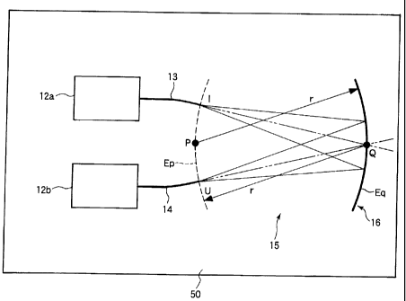
Fig. 1 shows a configuration of an optical signal
processing circuit constructed by coupling of two optical
waveguide circuitsl2a andl2b utilizing a reflectingstructure,
according to a first embodiment of the invention;
Fig. 2 shows a configuration of a laser ablation device
30 for forming a reflecting structure 16;
Fig. 3 is a sectional view of an optical waveguide substrate
50, which describes the steps of forming the reflectingstructure
16 on the optical waveguide substrate 50;
Fig. 4 shows a configuration of a 1:2 optical coupler
60 which is one of the detailed application examples of an optical
signal processing circuit according to the first embodiment;
Fig. 5 shows a modified version of the configuration of
the optical signal processing circuit constructed by coupling
of two optical waveguide circuits 12a and 12b utilizing the
reflecting structure shown in Fig. 1;
Fig. 6 shows a second embodiment of an optical signal
processing circuit constructed by coupling of two optical
waveguide circuits 12a and 12b utilizing the reflecting
structure 16;
Fig. 7 shows a modified version of the optical signal
19
CA 02433873 2003-06-25
processing circuit constructed by coupling two optical
waveguide circuits 12a and 12b utilizing the reflecting
structure shown in Fig. 6;
Fig. 8 shows a configuration of an N:N star-type optical
coupler 70 as a detailed application example of an optical signal
processing circuit according to the second embodiment which
is described with respect to Fig. 6;
Fig. 9 shows a third embodiment of an optical signal
processing circuit constructed by coupling of two optical
waveguide circuits 12a and 12b utilizing the reflecting
structure 16;
Fig. 10 shows a configuration of an optical wavelength
multiplexer 8 0 which is one of the detailed application examples
of the optical signal processing circuit according to the third
embodiment described with respect to Fig. 9;
Fig. 11 shows a configuration of another optical
wavelength multiplexer 80 which is one of the detailed
application examples of the optical signal processing circuit
according to the third embodiment described with respect to
Fig. 9;
Fig. 12 shows a detailed configurational example of a
periodic grooved structure 81;
Fig. 13 shows another detailed configurational example
CA 02433873 2003-06-25
of the periodic grooved structure 81;
Fig. 14 shows still another detailed configurational
example of the periodic grooved structure 81;
Fig. 15 shows a periodic grooved structure 81d having
a filler material 86, which is made of a polymer material or
dielectric material, filled up on the grooved portions 82;
Fig. 16 is a sectional view of the optical waveguide
substrate 50, which describes the steps of forming the periodic
grooved structure 81d on the optical waveguide substrate 50;
Fig. 17 shows a fourth embodiment of an optical signal
processing circuit constructed by coupling of two optical
waveguide circuits 12a and 12b utilizing the reflecting
structure 16;
Fig. 18 shows the details of an arcuate periodic grooved
structure 91 formed on the optical waveguide substrate 50;
Fig. 19 shows a fifth embodiment of an optical signal
processing circuit constructed by coupling of two optical
waveguide circuits 12a and 12b utilizing the reflecting
structure 16;
Fig. 20 shows a detailed configuration of an arrayed
waveguide 101;
Fig. 21 shows a sixth embodiment of an optical signal
processing circuit constructed by coupling of two optical
21
CA 02433873 2003-06-25
waveguide circuits 12a and 12b utilizing the reflecting
structure 16;
Fig. 22 is a sectional view of a wave front compensation
portion 111;
Fig. 23 shows a seventh embodiment of an optical signal
processing circuit constructed by coupling of two optical
waveguide circuits 12a and 12b utilizing the reflecting
structure 16;
Fig. 24 is a sectional viewof the optical signal processing
circuit shown in Fig. 23;
Fig. 25 shows a modified version of the configuration
shown in Fig. 23 and Fig. 24;
Fig. 26 shows an eighth embodiment of an optical signal
processing circuit constructed by coupling of two optical
waveguide circuits 12a and 12b utilizing the reflecting
structure 16;
Fig. 27 is a sectional view of the optical signal processing
signal shown in Fig. 26;
Fig. 28 shows a ninth embodiment of an optical signal
processing circuit constructed by coupling of two optical
waveguide circuits 12a and 12b utilizing the reflecting
structure 16;
Fig. 29 is a sectional view of the optical signal processing
22
CA 02433873 2003-06-25
signal shown in Fig. 28;
Fig. 30 shows a tenth embodiment of an optical signal
processing circuit having a pseudo phase matching structure
in which optical waveguides are connected in multiple stages,
utilizing the reflecting structure;
Fig. 31 shows an eleventh embodiment of an optical signal
processing circuit having a pseudo phase matching structure
in which optical waveguides are connected in multiple stages,
utilizing the reflecting structure;
Fig. 32 shows the details of a grooved structure 306;
Fig. 33 is a sectional view of an optical waveguide
substrate 50 for describing the steps of producing a further
minute structure than the wavelength km of a processing laser
beam by laser ablation processing;
Fig. 34 shows the details of a pattern of a thin film
54;
Fig. 35 shows a method for producing a sub-micron level
minute structure by an electron beam exposure method according
to a twelfth embodiment of the invention;
Fig. 36 shows a method for producing a sub-micron level
minute structure by an ion implantation method according to
a thirteenth embodiment of the invention;
Fig. 37 shows a method for producing a sub-micron level
23
CA 02433873 2003-06-25
minute refractive index controlling structure by a minute
pattern copying method according to a fourteenth embodiment
of the invention;
Fig. 38 shows a TE/TM mode splitting circuit constructed
by utilizing any one of the methods according to the eleventh
through thirteenth embodiments;
Fig. 39 shows the details of a mode separation structure
703;
Fig. 40 shows a first example of patterns for constructing
the mode separation structure 703;
Fig. 41 shows a second example of patterns for constructing
the mode separation structure 703;
Fig. 42 shows a configuration of a prior art slab waveguide
type lens functioning circuit; and
Fig. 43 shows a configuration of an optical nonlinear
element having a pseudo phase matching section according to
a prior art periodic polarization inverting structure 502.
DESCRIPTION OF REFERENCE NUMBERS
12 Optical waveguide circuit
13 Output waveguide
14 Input waveguide
15 Coupling circuit (Slab waveguide)
24
CA 02433873 2003-06-25
16 Reflecting structure
30 Laser ablation device
50 Optical waveguide substrate
51 Lower clad layer
52 Core layer
53 Upper clad layer
54 Thin film
55 Resist
56 Metal or dielectric film
57 Concave portion
60 1:2 optical coupler
70 N:N star-type optical coupler
80 Optical wavelength multiplexer
81 Periodic structure
82, 83, 84 Grooves
86 Filler
90 Optical wavelength multiplexer
91 Arcuate periodic grooved structure
101 Arrayed waveguide
302 Single mode optical waveguide
303 Slab waveguide
304 Periodic polarization inverting structure
305 Reflecting structure
CA 02433873 2003-06-25
306 Grooved structure
307 Side wall
401 Quartz substrate
402 Positioning pattern
403 Metal
404 Polymer waveguide substrate
701 Input waveguide
702 Reflecting structure
703 Mode separation structure
704 Output waveguide
705 High refractive index portion
706 Low refractive index portion
BEST MODE FOR CARRYING OUT THE INVENTION
Hereinafter, a detailed description is given of preferred
embodiments of the invention with reference to the accompanying
drawings.
In the description thereof, the same components and
elements are given the same reference numbers, and overlapping
description thereof is omitted.
Fig. 1 shows a configuration of an optical signal
processing circuit constructed by coupling of two optical
waveguide circuitsl2a andl2b utilizing a reflectingstructure,
26
CA 02433873 2003-06-25
according to a first embodiment of the invention.
Herein, the optical waveguide substrate 50 is provided
with the optical waveguide circuits 12a and 12b. And, the output
waveguide 13 and input waveguide 14 are, respectively, connected
to the optical waveguide circuits 12a and 12b at their one end
side, and are connected to the coupling circuit 15 at their
other end side.
Reference number 1 denotes an input coupling end (that
is, the output coupling end of the output waveguide 13) of the
coupling circuit 15 and output waveguide 13. U denotes the output
coupling end (that is, the input coupling end of the input
waveguide 14) of the coupling circuit 15 and input waveguide
14.
The coupling circuit 15 is constructed by a slab waveguide
15 in which the respective end faces Ep and Eq including the
axis ends P and Q with respect to the axis PQ are shaped so
as to become a prescribed curvature.
In the case of the present embodiment, the coupling circuit
15 is shaped so that the end face Ep including one axis end
P is made into a curved face whose curvature is r with the other
axis end Q made into the center of curvature, and the end face
Eq including the other axis end Q is made into a curved face
whose curvature is r with the other axis end P made into the
27
CA 02433873 2003-06-25
center of curvature.
The other end face Eq configures the reflecting structure
16 having a curvature r with the axis end P made into the center
of curvature.
In addition thereto, the input coupling end I (that is,
the output coupling end of the output waveguide 13) of the
coupling circuit 15 and the output coupling end U (that is,
the input coupling end of the input waveguide 14) of the coupling
circuit 15 are disposed so that these constitute linear symmetry
with the axis PQ made into the center line.
Thereby, with respect to the input coupling end I and
output coupling end U of the coupling circuit 15, either of
the optical axes of the input coupling end I and output coupling
end U will pass through the axis end Q on a reflecting structure
16 whose curvature is r.
Therefore, the optical axes of the input coupling end
I (that is, the output coupling end of the output waveguide
13) and output coupling end U (that is, the input coupling end
of the input waveguide 14) of the coupling circuit 15 pass through
the same point Q on the reflecting structure 16, and the lengths
IQ and QU of the respective optical axes are kept at the same
length.
A portion surrounded by the curvature including the arc
28
CA 02433873 2003-06-25
IPU and the curvature including an arc of the reflecting
structure 16 constitutes the slab waveguide 15.
In the arrangement, the input coupling end I and output
coupling end U are caused to establish a relationship by which
an image is formed at equal magnification, wherein the output
waveguide 13 and input waveguide 14 are coupled together at
a high coupling efficiency.
Fig. 2 shows a configuration of a laser ablation device
30 for forming a reflecting structure 16.
Herein, a femtosecond light source 31 that is constructed
by a titan sapphire laser, etc., is composed so that, in the
case of the present embodiment, for example, a pulse light beam
whose repetition frequency is 1kHz is generated and output at
a pulse width which is usually 50fs ( femtoseconds ) or so, wherein
pulse energy of 2mJ can be obtained.
A pulse light beam generated by the femtosecond light
source 31 is provided to a laser light transmission device 32
and is spatially transmitted, wherein the beam diameter is
widened by the laser light transmission device 32 so that the
light beam is not condensed to a small spot.
A pulse whose beam diameter is widened by the laser light
transmission device 32 is devised to be output to a dichroic
mirror 35 via a spatial filter 34 secured on the ablation device
29
CA 02433873 2003-06-25
body 33. The spatial filter 34 is disposed at the focusing
position at the rear side of a light condensing lens described
later. At this time, since the sectional amplitude profile of
the condensed pulse light beam is approximated by Fourier
transformation of the sectional amplitude profile on the spatial
filter 34, it is possible to control the sectional amplitude
profile of the condensed pulse light beam by applying an adequate
sectional amplitude profile to the pulse light beam by the
spatial filter 34. For example, in the case where a mirror is
formed, it is sufficient that the spatial filter 34 is designed
so that an amplitude profile expressed in terms of a sine function
can be obtained on a line orthogonal to the optical axis.
The dichroic mirror 35 is constructed so as to function
as a mirror with respect to light having a wavelength of the
pulse light beam and to have a characteristic of propagating
the light for the wavelength of an illumination light source.
And, the pulse light beam whose sectional amplitude profile
is controlled via the spatial filter 34 is guided to the light
condensing lens 36.
Also, illumination light f roma downward irradiation light
source 37 is supplied into the dichroic mirror 35 via a half
mirror 38, and the dichroic mirror 35 is constructed so as to
guide not only the pulse light beam but also illumination light
CA 02433873 2003-06-25
to the light condensing lens 36.
The light condensing lens 36 is devised so as to condense
and irradiate the pulse light beam and illumination light onto
the optical waveguide substrate 50, placed and fixed on a
micromotion stage 39, which is micromovably disposed at the
front-side focusing position with respect to the ablation device
body 33.
The irradiation position of the pulse light beam onto
the optical waveguide substrate 50 is made adjustable since
a controller 41 controls the micromotion of the micromotion
stage 39, on which the optical waveguide substrate 50 is placed
and fixed, according to image output such as a positioning
pattern and an area to be etched, etc., on the optical waveguide
substrate 50, which comes from a pickup camera 40 disposed on
the mirror face side opposite to the side, of the half mirror
38, where the downward irradiation light source 37 of the half
mirror 38 is provided.
Therefore, actuators of the pickup camera 40 and
micromotion stage 39 are connected to the controller 41, and
at the same time, the Femtosecond light source 31 is also
connected thereto. And, the controller 41 controls not only
micromotions of the micromotion stage 39 but also a period,
energy and number of pulses of the pulse light beam generated
31
CA 02433873 2003-06-25
by the Femtosecond light source 31. That is, the controller
41 carries out synthetic control with respect to production
of an optical signal processing circuit 10 on the optical
waveguide substrate 50.
By the laser ablation device 30 thus constructed, the
ref lecting structure 16 of the optical signal processing circuit
is formed by the following steps. In addition, the description
thereof is based on the assumption that the waveguide circuit
13 (or 14) is already produced on the optical waveguide substrate
50 in the previous step.
Fig. 3 is a sectional view showing an optical waveguide
substrate 50, whichdescribesthestepsofforming the reflecting
structure 16 on the optical waveguide substrate 50;
Fig. 3-(a) is a sectional view showing the optical
waveguide substrate 50 in which a waveguide circuit 13 (or 14)
is formed.
The waveguide circuit 13 (or 14) is formed by laminating
the lower clad layer 51, core layer 52, and upper clad layer
53 on the substrate 50 one after another in order.
First, when forming the reflecting structure 16, a metal
or dielectric thin film 54 is formed on the waveguide circuit
13 (or 14).
Thereafter, resist 55 is applied on the optical waveguide
32
CA 02433873 2003-06-25
substrate 50, and the metal or dielectric thin film 54 is coated
for processing by the resist 55 (See Fig. 3-(b)).
A pattern is traced on the resist 55 with an electron
beam tracing device (not illustrated).
The resist 55 is developed through EB exposure, and the
resist 55 existing on the etching plane is peeled off to carry
out patterning (See Fig. 3-(c)).
Using the resist 55 as a mask, the resist 55 is peeled
off by a reactive ion etching device (not illustrated), and
the exposed portionsare etched,wherein an electron beam tracing
pattern brought about by the electron beam tracing device is
copied on the thin film 54 (See Fig. 3-(d)).
After that, the resist 55 is peeled off from the optical
waveguide substrate 50 (See Fig. 3-(e)).
Furthermore, the electron beam tracing pattern is copied
onto the thin film 54, and the optical waveguide substrate 50
in which the resist 55 is peeled off is fixed on the micromotion
stage 39 of the laser ablation device 30.
A plurality of maker images provided on the optical
waveguide substrate 50 are observed by a monitoring device (not
illustrated) utilizing the pickup camera 40, and the tilt angle
is adjusted so that the optical waveguide substrate 50 becomes
perpendicular to the optical axis of the pulse light beam.
33
CA 02433873 2003-06-25
A plurality of markers provided on the optical waveguide
substrate 50 are similarly observed by a monitoring device,
and thestage controller (controller) 41 is rendered to recognize
the positions of the patterns.
According to control carried out by the controller 41,
the laser ablation device 30 condenses a pulse light beam
generated by the femtosecond light source 31 with the condensing
lens 36 and sweeps the surface of the optical waveguide substrate
50 by a spot of the pulse light beam by moving the micromotion
stage 39, thereby etching the upper clad layer 53, core layer
52 and lower clad layer 51 at the portion where the resist 55
is peeled off in the step. Also, the etching depth is controlled
by the number of times of irradiation of the pulse light beam
(Fig. 3-(f)).
After the etching is completed on the lower clad layer
51, core layer 52 and upper clad layer 53 according to the
patterning, the optical waveguide substrate 50 is removed from
the micromotion stage 39, and the remaining thin film 54 portion
is removed (Fig. 3-(g)).
Metal or dielectric film 56 is deposited on the end faces
57e of the etched concave portion 57, that is, the end faces
57e of the lower clad layer 51, core layer 52 and upper clad
layer 53, which are formed by the etching. The lift-off method
34
CA 02433873 2003-06-25
may be utilized in order to partially form a metal or dielectric
film 56 on the optical waveguide substrate 50 (Fig. 3-(h)).
In the procedure, an especially critical point is to select
a material of the thin film 54. It is necessary that the thin
film 54 is sufficiently thin with respect to the etching depth
and endures the irradiation of the pulse light beam. For this
reason, metal materials such as tantalum, molybdenum, tungsten,
chromium, gold, platinum, vanadium, nickel, silver, and copper
are suitable as the material of thin film 54 with respect to
the quartz-based waveguide, and dielectric materials such as
silicon oxide (SiOZ), silicon nitride (SiN), titanium oxide
(TiOz), boron nitride (BN), aluminium nitride (A1N) may be
acceptable with respect to polymer-based waveguides in addition
to the above-described metals.
Also, in the case of the polymer-based waveguide, etching
may be carried out using the resist 55 as a mask without utilizing
the thin film 54.
Further, where the beam profile of the laser ablation
device 30 approximates a rectangle, no mask is utilized as in
the above case, and it is possible that a grooved structure
is directly formed. The procedure in this case will be described
below.
First, the optical waveguide substrate 50 on which the
CA 02433873 2003-06-25
waveguide circuit 13 (or 14) is formed is fixed on the micromotion
stage 39.
A plurality of markers provided on the optical waveguide
substrate 50 are observed by the monitoring device, and the
tilt angle is adjusted so that the optical waveguide substrate
50 becomes perpendicular to the optical axis of the pulse light
beam.
Simultaneously, a plurality of markers provided on the
optical waveguide substrate 50 are similarly observed by the
monitoring device, and the stage controller (controller) 41
is rendered to recognize the positions of the waveguide circuit
13 (or 14).
Based on control made by the controller 41, the laser
ablation device 30 condenses a pulse light beam generated by
the femtosecond light source 31 with the light condensing lens
36 along the portion where the reflecting structure 16 is
provided, moves the micromotion stage 39 and prepares the concave
portion 57.
After that, this time, the laser ablation device 30
condenses a pulse light beam along the surroundings of the
concave portion 57, moves the micromotionstage39andsmoothens
the end face 57e of the concave portion 57.
Fig. 4 shows a configuration of a 1:2 optical coupler
3 6
CA 02433873 2003-06-25
60 which is one of the detailed application examples of an optical
signal processing circuit according to the first embodiment.
Herein, the reflecting structure 16 is divided into two
reflecting structures 16-1 and 16-2 whose center points differ
from each other, at the boundary point Qo. The first reflecting
structure 16-1 is composed of a spherical surface including
an arc QoQl whose curvature radius is r, centering around the
point P1, and the second reflecting structure 16-2 is composed
of a spherical face including an arc QoQ2 having a curvature
radius r of the same size, centering around the point PZ.
The center points P1 and P2 are provided on the circumference
having a radius r of the same size centering around the boundary
point Qo of the first and second reflecting structure 16-1 and
16-2, and the input coupling end I (that is, the output coupling
end of the output waveguide 13) of the coupling circuit 15 and
the output coupling end U (that is, the input coupling end of
the input waveguide 14) thereof, respectively, meet the
positional relationship that is similar to that in the case
of the reflecting structure 16 shown in Fig. 1.
That is, the optical axis of the input coupling end I
(that is, the output coupling end of the output waveguide 13)
of the coupling circuit 15 is disposed on the circumference
of radius r passing through the points Pl and P2 centering around
37
CA 02433873 2003-06-25
the boundary point Qo so that it passes through the boundary
point Qo of the reflecting structure 16.
In addition thereto, the first output coupling end U1
(that is, the first input coupling end of the input waveguide
14) of the coupling circuit 15 is disposed on the line including
the boundary point Qo of the reflecting structure 16 and the
center P. of an arc of the first reflecting structure 16-1,
that is, on the circumference of radius r passing through the
points P1 and PZ centering around the boundary point Qo, which
is linearly symmetrical to the input coupling end I (that is,
the output coupling end of the output waveguide 13) of the
coupling circuit 15.
To the contrary, the second output coupling end U2 (that
is, the second input coupling end of the input waveguide 14)
of the coupling circuit 15 is disposed on the line including
the boundary point Qo of the reflecting structure 16 and the
center point P2 of an arc of the second reflecting structure
16-2, that is, on the circumference of radius r passing through
the points P1 and P2 centering around the boundary point Qo,
which is linearly symmetrical to the input coupling end I (that
is, the output coupling end of the output waveguide 13) of the
coupling circuit 15, centering the axis P2Q1.
The portion surrounded by the curvature consisting of
38
CA 02433873 2003-06-25
these arcs is made into a slab waveguide 15.
Resultantly, since the input coupling end I of the coupling
circuit 15 and the first output coupling end U1 thereof, and
the input coupling end I of the coupling circuit 15 and the
second output coupling end U2 thereof are in a position where
an image-formation of each other is established via the first
reflecting structure 16-1 consisting of an arc QoQ1 and the second
reflecting structure 16-2 consisting of an arc QoQ2, one half
of the emission light from the input coupling end I is distributed
to the first output coupling end U1 and the second output coupling
end U2, and the optical signal processing circuit according
to the present embodiment functions as a 1:2 optical coupler
60 that bifurcates an incident light at the ratio of 1:1.
Also, the 1:2 optical coupler 60 according to the
embodiment is formed so that the center point of the first
reflecting structure 16-1 consisting of an arc QoQl is made into
P1, and the center point of the reflecting structure 16-2
consisting of an arc QoQ2 is made into P2 . However, even if the
first reflecting structure 16-1 consisting of arc QoQl is formed
with the center point made into P2, and the second reflecting
structure 16-2 consisting of arc QoQ2 is formed with the center
point made into P1, a 1:2 optical coupler having a function
similar to that of the 1: 2 optical coupler 60 can be constructed.
39
CA 02433873 2003-06-25
Further, in the 1:2 optical coupler 60 according to the
embodiment, it is a matter of course that a 1:2 optical coupler
60 which distributes light at an arbitrary ratio can be produced
by adjusting the division position of the reflecting structure
16.
Fig. 5 shows a modified version of the configuration of
an optical signal processing circuit constructed by coupling
two optical waveguide circuits 12a and 12b utilizing the
reflecting structure shown in Fig. 1.
In the optical signal processing circuit shown in Fig.
1, the description was given of the case where the intersection
line of the reflecting structure 16 and plane including the
waveguides 13 and 14 is an arc. However, in the optical signal
processing circuit shown in Fig. 5, the intersection line of
the reflecting structure 16 and the planes including the
waveguide lines 13 and 14 is made elliptically arcuate, wherein
the input coupling end I of the coupling circuit 15 and the
output coupling end U thereof are made into focusing points.
In this case, where the point at which the optical axis
of the input coupling end I of the coupling circuit 15 is crossed
with that of the output coupling end U thereof is made into
Q, the center of an ellipse is made into S, and the minor diameter
"b" is expressed in terms of line QS, the distance IS between
CA 02433873 2003-06-25
the input coupling end I and center point S is the same length
"c" as the distance US between the output coupli.ng end U and
the center point S. Further, if the maj or diameter of the ellipse
is "a," the length "c" meets the relationship expressed by the
following expression:
c = aa- ba (1)
The reflecting structure 16 is made into an elliptically
arcuate curvature having such a relationship.
Also, the curvature of the reflecting structure 16 is
not limited to such an elliptical arcuate shape and the
above-described arc. It may be a quadratic optical reflective
system expressed by other quadratic curves such as a curvature
that is expressed by, for example, a parabola and a hyperbola.
Further, in the quadratic optical reflective system in
which the reflecting structure 16 shown in Fig. 1 and Fig. 5
is expressed by a quadratic curve including a circular arcuate
shape such as an arc or ellipse, a description was given of
a configuration of an imaging optical system of equal
magnification as an example. However, an imaging optical system
of an arbitrary magnification may be constructed.
In this case, in Fig. 1 and Fig. 5, the optical axis of
the input coupling end I of the coupling circuit 15 and the
41
CA 02433873 2003-06-25
optical axis of the output coupling end U thereof pass through
the same point Q on the reflecting structure 16, and it is
sufficient that the following expression is established with
respect to the distance IQ between the input coupling end I
and point Q and the distance QU between the point Q and the
output coupling end U.
+ 1 ^2 (2)
IQ UQ r
Fig. 6 shows the second embodiment of an optical signal
processing circuit constructed by coupling of the two optical
waveguide circuits 12a and 12b utilizing the reflecting
structure 16.
The reflecting structure 16 is composed of a sphere
composed of an arc of curvature radius r centering around the
point P. The point Q shows the point on the arc of the reflecting
structure 16.
Herein, point T is an end point obtained by extending
a segment PQ in the direction of the point Q by a distance of
r/2, and the respective centers of the input coupling end I
of the coupling circuit 15 and output coupling end U thereof
are disposed on the circumference of radius r centering around
the end point T. In addition thereto, the optical axis of the
input coupling end I (that is, the output coupling end of the
42
CA 02433873 2003-06-25
output waveguide 13) and the optical axis of the output coupling
end U (that is, the input coupling end of the input waveguide
14) of the coupling circuit 15 are disposed so that each thereof
passes through the point Q.
The portion surrounded by a curvature consisting of an
arc of radius r making the point Q and end point T into the
respective centers is made into a slab waveguide 15, and becomes
a portion for propagating light.
At this time, the input coupling end I of the slab waveguide
(coupling circuit) 15 and the output coupling end U thereof
are, respectively, positioned in the relationship of spatial
Fourier transformation.
Fig. 7 shows a modified version of the configuration of
the optical signal processing circuit constructed by coupling
of two optical waveguide circuits 12a and 12b utilizing the
reflecting structure shown in Fig. 6.
In the optical signal processing circuit shown in Fig.
6, a description was given of the case where the intersection
line between the reflecting structure 16 and a plane (that is,
the plane including the optical axes of the input coupling end
I and output coupling end U of the coupling circuit 15) including
the waveguides 13 and 14 is an arc. However, in the optical
signal processing circuit shown in Fig. 7, the intersection
43
CA 02433873 2003-06-25
line between the reflecting structure 16 and plane including
the waveguides 13 and 14 is devised so as to be expressed by
another quadratic curve, for example, a parabola.
That is, in Fig. 7, the reflecting structure 16 is made
like a parabola in which the input coupling end I of the coupling
circuit 15 is made into the focus, and the top point Q of the
parabola in which the optical axis of the input coupling axis
I crosses the reflecting structure 16 is made into a notched
portion 65, in which a reflected return light is reduced, by
removing the reflecting structure 16.
Fig. 8 shows a configuration of an N:N star-type optical
coupler 70 which is a detailed application example of the optical
signal processing circuit according to the second embodiment,
which is described with respect to Fig. 6.
In the configuration, the output waveguide 13 and input
waveguide 14 are, respectively, an array consisting of N
waveguides.
Light emitted from one waveguide of the output waveguide
13 is converted to parallel light by the reflecting structure
16, and is distributed to respective waveguides of the input
waveguide 14.
In this case, since it is necessary that light is
distributed to all the waveguides, the curvature r of the
44
CA 02433873 2003-06-25
reflecting structure 16 and the widths D of the output waveguide
13 and input waveguide 14 is in a fixed relationship shown by
the following expression:
rty. > D (3)
zn,.2
where c.oc is a mode radius of light propagating in the
waveguides of the output waveguide 13 and input waveguide 14,
a, is a wavelength, nc is an effective refractive index of the
slab waveguide 15, and r is a curvature radius.
Since the input coupling end I of the slab waveguide 15
and the output coupling end U thereof are, respectively, in
the relationship of Fourier transformation, the mode profile
in the vicinity of the emission end of the output waveguide
13 and input waveguide 14 is controlled in order to reduce the
range in the coupling efficiency between waveguides or to
increase the coupling efficiency. For example, in the case of
increasing the coupling efficiency, the end of the waveguide
may be widened to be tapered.
In the prior art configuration shown in Fig. 42, since
the input and output waveguides 201a and 201b are radially
connected to the slab waveguide 202, no isochronism is met at
a point on a specified line perpendicular to the optical axis.
To the contrary, light guided on line X in Fig. 8 at a
CA 02433873 2003-06-25
specified time simultaneously crosses the line Y at another
specified time, wherein isochronism is established. In several
optical signal processes, the isochronism is an important
feature in view of matching optical pulse positions, that is,
rise and fall timing of a pulse.
In addition, in the detailed application example, since
the curvature radius r can be made comparatively large, and
the respective coupling waveguides of the output waveguide 13
and input waveguide 14 are linearly disposed in parallel to
each other, it becomes easy to design and produce the optical
signal processing circuit.
Fig. 9 shows the third embodiment of the optical signal
processing circuit constructed by coupling of two optical
waveguide circuits 12a and 12b utilizing the reflecting
structure 16.
In the construction, as in the configuration of the optical
signal processing circuit shown in Fig. 6, the input coupling
end I1 (that is, the output coupling end of the output waveguide
13) of the first coupling circuit 15a and the input coupling
end U1 (that is, the output coupling end of the first coupling
circuit 15a) of the optical waveguide circuit 12c, and the output
coupling end 12 (that is, the input coupling end of the second
coupling circuit 15a) and the output coupling end U2 (that is,
46
CA 02433873 2003-06-25
the input coupling end of the input waveguide 14) of the second
coupling circuit 15a are, respectively, positioned in the
relationship of spatial Fourier transformation.
Thereby, emission light from the output waveguide 13
becomes a parallel light whose light beam diameter is widened
by the first reflecting structure 16a of the first coupling
circuit 15a, and is made incident into the optical waveguide
circuit 12c. At this time, since the light becomes a wide light
beam in the slab waveguide 15 (that is, the waveguide including
the first and second coupling circuits 15a and 15b, and the
optical waveguide circuit 12c) , no large loss is produced even
if optical components whose size is several tens of microns
or more, such as a wavelength plate, phase element, Faraday
element, polarization plate, etc., are disposed at the position
of the optical waveguide circuit 12c instead of the optical
waveguide circuit 12c, wherein it becomes possible to dispose
these components.
The emission light from the optical waveguide circuit
12c, that is, a wide light beam in the slab waveguide 15 (that
is, the waveguide including the first and second coupling
circuits 15a and 15b and the optical waveguide circuit 12c)
is condensed by the second reflecting structure 16b of the second
coupling circuit 15b and is input into the input waveguide 14.
47
CA 02433873 2003-06-25
Fig. 10 and Fig. 11 show a configuration of the optical
wavelength multiplexer 80, which is one of the detailed
application examples of the optical signal processing circuit
according to the third embodiment described with reference to
Fig. 9.
Herein, in the optical wavelength multiplexer 80 in Fig.
and Fig. 11, a periodic grooved structure 81 is disposed
as the optical waveguide circuit 12c. Fig. 10 shows a case where
the periodic grooved structure 81 is parallel to the optical
axis of the parallel light while Fig. 11 shows a case where
the periodic grooved structure 81 is inclined with respect to
the optical axis of the parallel light.
Fig. 12 through Fig. 14 show detailed configurational
examples of the periodic grooved structure 81.
The periodic grooved structure 81a shown in Fig. 12 is
configured so that grooves 82 are juxtaposed to each other with
the groove width (concave portion width) of "d" and groove
spacing (convex portion width) of "d/nc," where nc is an
effective refractive index of the waveguide.
To the contrary, the periodic grooved structure 81d shown
in Fig. 13 is configured so as to become like a grating 85 in
which two types of grooves 83 and 84 parallel to each other
are crossed in a plurality at a prescribed angle.
48
CA 02433873 2003-06-25
In the embodiment, the groove 83 is formed on the optical
waveguide substrate 50 with the groove width (concave portion
width) of "d" and the groove spacing (convex portion width)
of "d/nc" while the groove 84 is formed on the optical waveguide
substrate 50 with the groove width (concave portion width) of
"dl " and the groove spacing (convex portion width) of N'd' /nc, "
wherein both the grooves 83 and 84 are formed with the groove
width (concave portion width) and groove spacing (convex portion
width) different from each other.
Also, the periodic grooved structure 81c shown in Fig.
14 is configured so that the groove width "d" (concave portion
width) of the groove 82 and grating 85 and the groove spacing
"d/nc" (convex portion width) are not fixed, but the groove
width "d" (concave portion width) and groove spacing "d/nc"
(convex portion width) may vary.
Procedures for producing the periodic grooved structure
81 on these optical waveguide substrates 50 are similar to the
procedures for producing grooves on the optical waveguide
substrate 50 for the above-described reflecting structure 16.
In the grating of these periodic grooved structures 81,
the diffraction characteristics show generally intensive
wavelength-angle dependence, and diffract light of a specified
wavelength to a specified angle.
49
CA 02433873 2003-06-25
In particular, since, in the periodic grooved structures
81, there exist two types of fundamental gratings, diffraction
corresponding to the respective gratings appears so as to overlap
each other. Theref ore, complicated wavelength-angle dependence
can be brought about.
In addition, dilatory wavelength-angle dependence can
be brought about in the periodic grooved structure 81c.
In the optical wavelength multiplexer 80 described with
reference to Fig. 10 and Fig. 11, the reflecting structure 16
depends on a wavelength that transforms a change in angle to
a change in the light condensing position, and light is coupled
in different waveguides of the input waveguide 14. That is,
the optical signal processing circuit configured in Fig. 10
and Fig. 11 functions as an optical wavelength multiplexer
circuit.
Further, in order to protect the periodic grooved
structure 81 portion and to control the characteristics thereof,
there may be a case where a polymer material or a dielectric
material is filled up in the groove 82 portions (concave
portions).
Fig. 15 shows a periodic grooved structure 81d in which
a filler 86 consisting of a polymer material and a dielectric
material is filled up in the grooved portions 82.
CA 02433873 2003-06-25
In the periodic grooved structure 81d, since a change
in the refractive index is slight, very keen wavelength-angle
dependence can be brought about. Procedures for producing such
a periodic grooved structure 81 are almost identical to those
for producing the ref lecting structure 16. However, hereinafter,
a description is given of the procedures.
Fig. 16 is a sectional view showing the optical waveguide
substrate 50 in order to describe the steps for forming a periodic
grooved structure 81d on the optical waveguide substrate 50.
A waveguide circuit 13 (or 14) is formed on the substrate
50, and the waveguide circuit 13 (or 14) is formed by laminating
the lower clad layer 51, core layer 52, and upper clad layer
53 one after another (Fig. 16-(a)).
First, when forming the reflecting structure 16, a metal
or dielectric thin film 54 is formed on the waveguide circuit
13 (or 14).
After that, resist 55 is applied on the optical waveguide
substrate 50, and a metal or dielectric thin film 54 is cladded
with the resist 55 for processing (Fig. 16-(b)).
A pattern is traced on the resist 55 with an electron
beam tracing device, and the resist 55 is developed (Fig.
16- (c) ) .
The thin film 54 is etched by a reactive ion etching device,
51
CA 02433873 2003-06-25
using the resist 55 as a mask, and an electron beam tracing
pattern is copied (Fig. 16-(d)).
Thereafter, the remaining resist 55 is peeled off (Fig.
16- (e) ) .
In addition thereto, the optical waveguide substrate 50
is fixed on the micromotion stage 39 of the laser ablation device
30.
Observing a plurality of markers provided on the optical
waveguide substrate 50 by a monitoring device, the tilt angle
of the micromotion stage 39 is adjusted so that the optical
waveguide substrate 50 becomes perpendicular to the optical
axis of a pulse light beam.
Similarly, observing a plurality of markers provided on
the optical waveguide substrate 50 by a monitoring device, the
stage controller (controller) 41 is rendered to recognize the
position of the above-described pattern.
After that, the pulse light beam is condensed by the light
condensing lens 36, and the surface is swept by a spot of the
pulse light beam by moving the micromotion stage 39 in order
to carry out etching ( Fig . 16- ( f)). At this time, the etching
depth is controlled by the number of times of pulse irradiation.
After the etching is completed, the optical waveguide
substrate 50 is removed from the micromotion stage 39, and the
52
CA 02433873 2003-06-25
thin film 54 is removed (Fig. 16-(g)).
After that, a filler 86 consisting of a polymer material
and a dielectric material is filled up in the grooved portions
82 that constitute the periodic grooved structure 81. This is
carried out by deposition or spin coating (Fig. 16-(h)).
Fig. 17 shows the fourth embodiment of the optical signal
processing circuit constructed by coupling of two optical
waveguide circuits 12a and 12b utilizing the reflecting
structure 16.
The optical signal processing circuit according to the
embodiment substitutes the reflecting structures 16-1 and 16-2
shown in Fig. 4 into an arcuate or quadratic curve-like periodic
grooved structure 91, and constitutes an optical wave
multiplexer 90.
Herein, with respect to a change in the periodic refractive
index, it is known that light having a wavelength in the vicinity
of Bragg wavelength corresponding to the period thereof is
selectively reflected. That is, it is possible to regard the
arcuate or quadratic curve-like periodic grooved structure as
a wavelength selecting reflecting structure, and it is possible
to constitute an optical wavelength multiplexer 90 by utilizing
the positional relationship shown in Fig. 4.
In Fig. 17, on the optical waveguide substrate 50, the
53
CA 02433873 2003-06-25
arcuate periodic grooved structures 91a, 91b and 91c are
concentrically formed with spacing therebetween, and the
reflecting structure 16 is also concentrically disposed at the
outer circumferential portion thereof.
Awavelength X1 component of emission light from the output
waveguide 13 is reflected by the arcuate periodic grooved
structure 91a and is coupled to the input waveguide 14a.
Similarly, a wavelength X2 component is reflected by the arcuate
periodic grooved structure 91b and is coupled to the input
waveguide 14b. A wavelength X3 component is reflected by the
arcuate periodic grooved structure 91c and is coupled to the
input waveguide 14c.
The remaining wavelength components are reflected by the
reflecting structure 16 and are coupled to the input waveguide
14d.
Fig. 18 shows the details of the arcuate periodic grooved
structure 91 formed on the optical waveguide substrate 50.
Fig. 18 presents a configuration in compliance with the
periodic grooved structure 81d shown in Fig. 15. However, it
is a matter of course that Fig. 18 may be constructed like the
periodic grooved structure 81a shown in Fig. 12.
In the embodiment, in order to narrow the bandwidth, a
grooved structure in which etching is carried out halfway to
54
CA 02433873 2003-06-25
the core layer 52 formed on the optical waveguide substrate
50 may be utilized. Different from the reflecting structure
16, the reflection point of the arcuate periodic grooved
structure 91 changes depending on the wavelength and a difference
in the refractive index between the end face 94 of the grooved
portion (concave portion) 92 of the arcuate periodic grooved
structure 91 and the between-groove portions (convex portion)
95. Therefore, it is necessary to determine the period depending
on the center wavelength to be coupled or split. Generally,
the period p is established to one-half the length of the light
wavelength in a waveguide with respect to the wavelength to
be reflected.
A
2 (4)
p= + n (in the case of the cyclic grooved structure 81a) (5)
.
p= a+ d (in the case of the cyclic grooved structure 81d) (5)'
n., n.
In expression (5)', ny is an effective refractive index
of the portion etched halfway to the core layer. The reflection
point is calculated by obtaining multiple reflection from the
boundary of the entire periodic grooved structure including
the phase. Also, although the structure of the periodic grooved
CA 02433873 2003-06-25
structure 81c may be applicable, the period is not fixed in
this case, and cannot be simply brought into a formula.
Further, since the periodic grooved structure 81a and
periodic grooved structure 81c overlap each other to constitute
the periodic grooved structure 81b, it is possible to utilize
the structure of the periodic grooved structure 81b. In this
case, Fig. 18 shows a state where the arcuate periodic grooved
structure 91 partially overlaps.
In addition, in the embodiment, since the arcuate periodic
grooved structure 91 utilizes a grooved structure etched halfway
to the core layer 52 formed on the optical waveguide substrate
50 in order to narrow the bandwidth, etching is carried out
halfway to the upper clad layer 53 in order to further narrow
the bandwidth, and a filler 86 consisting of a polymer material
and a dielectric material may be f illed up in the grooved portions
(concave portions) 92. To the contrary, in order to make the
bandwidth wider, etching is carried out halfway to the lower
clad layer 51 and a filler 86 consisting of a polymer material
and a dielectric material is filled up on the grooved portions
(concave portions) 92.
Further, in the embodiment, a description was given of
the periodic grooved structure 91, exemplifying the arcuate
structure as illustrated. However, the periodic grooved
56
CA 02433873 2003-06-25
structure 91 may be like a quadratic curve such as a parabolic
curve, elliptical curve, and hyperbolic curve.
Fig. 19 shows the fifth embodiment of the optical signal
processing circuit constructed by coupling of two optical
waveguide circuits 12a and 12b utilizing the reflecting
structure 16.
Topologically, the configuration of the embodiment is
equivalent to the embodiment shown in Fig. 9. However, since
the configuration is particularly useful, it is shown as a
separate embodiment.
The present configuration is an arrayed waveguide
diffraction grating 100 that utilizes the reflecting structure
16 and is provided with an arrayed waveguide 101.
Fig. 20 shows a detailed configuration of the arrayed
waveguide 101.
The arrayed waveguide 101 is composed of parallel
waveguide portions 102 and 104 and an arcuate or quadratic
curve-like waveguide portionl03. Where it is assumed that the
distance between the centers of respective waveguides of the
arrayed waveguide 101 is "h, " and the widening angle of an arc
of the arcuate waveguide portion 103 is 0, a difference L in
the optical path length between the respective waveguides is
expressed by the following expression:
57
CA 02433873 2003-06-25
(6)
L = n,,h8 (6)
Since there is a difference L in the optical path according
to the expression (4) although light emitted from the output
waveguide 13 is distributed to respective waveguides of the
arrayed waveguide 101 and is made incident at an equal phase,
the emission portion of the arrayed waveguide 101 is inclined,
depending on the wavelength, and the equal phase plane is
inclined on the plane 12. In the second reflecting structure
16b, a change in the incident angle is converted to a change
in the light condensing position on the output coupling end
U2 of the input waveguide 14. That is, the circuit of this
configuration functions as an optical multiplexer.
Fig. 21 shows the sixth embodiment of the optical signal
processing circuit constructed by coupling of two optical
waveguide circuits 12a and 12b, utilizing the procedures of
forming the periodic grooved structure 81d on the optical
waveguide substrate 50, which is described with reference to
Fig. 16.
The optical signal processing circuit according to the
embodiment is featured in that a wave front compensating portion
111 to reduce aberration which a general optical system has
is formed at the slab waveguide 15 portion of a quadratic curve
optical system in which the reflecting structure 16 shown in
58
CA 02433873 2003-06-25
Fig. 1 and Fig. 5 is expressed by a quadratic curve including
an arcuate shape such as an arc or ellipse. The wave front
compensating portion 111 is integrally formed on the optical
waveguide substrate 50 having an optical signal processing
circuit formed therein.
Fig. 22 is a sectional view showing the wave front
compensating portion 111 that is formed at the slab waveguide
15 portion on the optical waveguide substrate 50 so as to cross
the optical axis of the input coupling end I of the coupling
circuit 15.
As in the method for producing a periodic grooved structure
81 which is described with reference to Fig. 16, the wave front
compensating portionlllisproduced by removing a partialplane
of the upper clad layer 53, core layer 52 and lower clad layer
51 at the slab waveguide 15 portion to a prescribed pattern,
forming a wave front compensating portion forming groove 112,
and filling the wave front compensating portion forming groove
112 with a material 113 having a refractive index different
from that of the effective refractive index of the waveguide
consisting of the above-described upper clad layer 53, core
layer 52 and lower clad layer 51. The wave front compensating
portion forming groove 112 is devised so that the groove width
thereof changes depending on the positions in the lengthwise
59
CA 02433873 2003-06-25
-~~'C~i ~ ~~~~~=
direction.
Also, the place where the wave front compensating portion
111 is provided is not limited to the above-described position
but may be formed at the slab waveguide 15 portion on the optical
waveguide substrate 50 so as to cross the optical axis of the
output coupling end U of the coupling circuit 15.
Fig. 23 shows the seventh embodiment of the optical signal
processing circuit constructed by coupling of two optical
waveguide circuits 12a and 12b utilizing the reflecting
structure 16.
Fig. 24 is a sectional view showing the optical signal
processing circuit shown in Fig. 23.
In the configuration, as in the configuration of the
optical signal processing circuit shown in Fig. 6 and Fig. 9,
the input coupling end I1 (that is, the output coupling end
of the output waveguide 13) of the first coupling circuit 15a
and the input coupling end U1 (that is, the output coupling
end of the first coupling circuit 15a) , and the output coupling
end 12 (that is, the input coupling end of the second coupling
circuit 15a) and the output coupling end U2 (that is, the input
coupling end of the input waveguide 14) of the second coupling
circuit 15a are, respectively, positioned in the relationship
of spatial Fourier transformation.
--__ _ i - ------- _ _____
CA 02433873 2003-06-25
Thereby, emission light from the output waveguide 13 is
made incident into the optical waveguide circuit 12c by the
first reflecting structure 16a. In this case, the emission light
becomes a wide light beam in the slab waveguide 15 (that is,
the first and second coupling circuits 15a and 15b, and waveguide
including the optical waveguide circuit 12c) and widens the
light beam diameter in the optical waveguide circuit 12c in
which a partial plane of the upper clad layer 53, core layer
52, lower clad layer 51 and the optical waveguide substrate
50 is removed to a prescribed pattern at the slab waveguide
15 portion. Simultaneously, the emission light widens a light
beam in the direction perpendicular to the surface of the
waveguide of the optical waveguide circuit 12c between a pair
of cylindrical lenses 122 and 123 in the optical waveguide
circuit 12c by the cylindrical lenses 122 and 123 spaced from
each other and fixed in the grooved structure 121 of the optical
waveguide circuit 12c, wherein it becomes possible to
incorporate a comparatively large optical component 124
therein.
At this time, at the optical component 124, a component
may be diagonally inclined and attached with respect to the
direction of the light beam in order to suppress reflection
at the end face thereof.
61
CA 02433873 2003-06-25
Fig. 25 shows a modified version of the configuration
shown in Fig. 23 and Fig. 24.
In the configuration, cylindrical distribution
refractive index lenses 125 and 126 are spaced from each other
and attached in the light beamdirection in the grooved structure
121 instead of the cylindrical lenses 122 and 123.
In this case, a transparent adhesive agent 127 whose
refractive index is close to the refractive index of the
distribution ref ractive index lenses 125, 12 6 and slab waveguide
15 are utilized when fixing the distribution refractive index
lenses 125 and 126 in the grooved structure 121. If the
transparent adhesive agent 127 is further f illedinthe clearance
in the grooved structure 121 after the distribution refractive
index lenses 125 and 126 are fixed, no reflection preventing
film, etc., is required on the surface of the distribution
refractive index lenses 125 and 126, wherein solid fixing thereof
can be secured.
Fig. 26 shows the eighth embodiment of the optical signal
processing circuit constructed by coupling of two optical
waveguide circuits 12a and 12b utilizing the reflecting
structure 16.
Fig. 27 is a sectional view showing the optical signal
processing circuit shown in Fig. 26.
62
CA 02433873 2003-06-25
In the configuration, with respect to emission light from
the output waveguide 13, a light beam is condensed by the
reflecting structure 16a, and at the same time, the light beam
is condensed in the direction perpendicular to the surface of
the waveguide of the optical waveguide circuit 12c by a pair
of cylindrical lenses 128 and 129 spaced from each other and
fixed in the grooved structure 121 of the optical waveguide
circuit 12c in which a partial plane of the upper clad layer
53, core layer 52, lower clad layer 51 and optical waveguide
substrate 50 is removed to a prescribed pattern at the slab
waveguide 15 portion, wherein it becomes possible to incorporate
an optical component 130 such as a semiconductor laser, etc.,
between the cylindrical lenses 128 and 129.
At this time, at the optical component 130, a component
may be diagonally inclined and attached with respect to the
direction of the light beam in order to suppress reflection
at the end face thereof.
Fig. 28 shows the ninth embodiment of the optical signal
processing circuit constructed by coupling of two optical
waveguide circuits 12a and 12b utilizing the reflecting
structure 16.
Fig. 29 is a sectional view showing the optical signal
processing circuit shown in Fig. 28.
63
CA 02433873 2003-06-25
In the configuration, the emission light from the output
waveguide 13 is made into a parallel light whose light beam
diameter is widened by the reflecting structure 16a, and
simultaneously, a light beam is condensed in the direction
perpendicular to the surface of the waveguide of the optical
waveguide circuit 12c by a pair of cylindrical lenses 131 and
132 that are spaced from each other and fixed in the grooved
structure 121 of the optical waveguide circuit 12c in which
a partial plane of the upper clad layer 53, core layer 52, lower
clad layer 51 and the optical waveguide substrate 50 is removed
to a prescribed pattern on the slab waveguide 15 portion, wherein
it becomes possible to incorporate an optical component 133
such as a photo diode array, etc., between the cylindrical lenses
131 and 132.
At this time, at the optical component 133, a component
may be diagonally inclined and attached with respect to the
direction of the light beam in order to suppress reflection
at the end face thereof.
Fig. 30 shows the tenth embodiment of the optical signal
processing circuit having a pseudo phase matching structure
in which optical waveguides are connected in multiple stages
by utilizing the reflecting structure. Herein, the optical
waveguide substrate 50 is made of LiNb03 in the present embodiment.
64
CA 02433873 2003-06-25
Also, in single-mode optical waveguides 302a through 302e, the
cores thereof are formed by diffusing titanium. Slab waveguides
303a and 303b are also constructed by diffusing titanium. In
addition, a periodic polarization inverting structure 304 is
a pseudo phase matching section in which polarization is
periodically inverted. Since a wavenumber corresponding to the
period compensates a difference between two times the
propagation coefficient of basic waves and the propagation
coefficient of the secondary harmonics, for example, in
generation of the secondary harmonics, it is possible to achieve
the phase matching in a long area. The reflecting structures
305a through 305d couple between respective single-mode
waveguides. Generally, the efficiency of the secondary optical
nonlinear effect (secondary harmonics generation,
sum-frequency generation, differential-frequency generation,
and parametric amplification, etc.,) is proportional to the
square of the length of the waveguide. Conventionally, it is
expected that the efficiency which has been limited by the size
of a substrate can be dramatically increased by a lengthening
of the size thereof, which is brought about by multiple-stage
connections using the reflecting structures 305a through 305d.
That is, according to the present embodiment,for example, under
the condition that the nonlinear effect is not saturated, the
CA 02433873 2003-06-25
efficiency is increased twenty-five times (5 x 5) Utilizing
these effects,it becomes possible to construct an optical signal
processing circuit that is able to obtain short wavelength laser
light necessary for wavelength conversion and optical memory
in optical communications by secondary harmonics generation.
The method and structure for producing the reflecting
structures 305a through 305d are the same as those in the first
and second embodiments, and the description thereof is omitted.
The present embodiment has achieved an optical nonlinear
circuit that increases mutual operating lengths by providing
a number of reflecting structures 305a through 305d on the
optical waveguide substrate 50 and includes a pseudo phase
matching section brought about by a highly efficient periodic
polarization inverting structure. Since a fold-over structure
brings about multiple stages even if the optical waveguide
substrate is small-sized, an increase in the mutual operating
length can be achieved. Since the efficiency of the nonlinear
element is proportional to the square of the length, it is
possible to raise the efficiency 10 through 100 times and
increase the same to the saturation range. That is, it becomes
possible to carry out wavelength conversion and to generate
secondary harmonics at low pumping power, wherein circuits can
be made small-sized, power consumption can be decreased and
66
CA 02433873 2003-06-25
noise level can be also reduced.
Fig. 31 shows the eleventh embodiment of the optical signal
processing circuit having a pseudo phase matching structure
in which optical waveguides are connected in multiple stages
utilizing the reflecting structure. Herein, as shown in Fig.
32, a grooved structure 306 is formed, which cuts off the core
portions of the single-mode optical waveguides 302a through
302i, and the side wall 307 thereof is functioned as the entire
reflection mirror, whereby an optical signal processing circuit
isconstructed,which includes a pseudo phase matching structure
in which the single-mode waveguides 302a through 302i are
connected in multiple stages. Generally, since the refractive
index of the material of the waveguide is sufficiently higher
than the refractive index of air, a high reflection factor can
be obtained with any metal layer provided on the side wall.
However, a protection film such as a metal layer may be provided
to protect the side thereof.
In the embodiment, a description is based on an example
using an LiNbO3 waveguide of titanium diffused core. However,
it is a matter of course that Mg-doped LiNbO3, LiTaO3, KTiOPO4,
and RbTiOPO4 may be used. Also, as a matter of course, Li-proton
exchange may be used for core layer production.
In the method according to the present embodiment, a minute
67
CA 02433873 2003-06-25
structure producing method is made clear, which utilizes a
pattern whose length has the wavelength of a processing laser
wavelength or longer with respect to one direction and has the
wavelength or less with respect to another direction, in order
to achieve laser processing less than the sub-micron level.
In almost all optical signal processing circuits, if the minute
direction of a pattern is made coincident with the propagation
direction of signal light since the propagation direction of
signal light is one direction, it becomes possible to achieve
a sufficiently minute structure with respect to signal light.
For example, it becomes possible to vary and control the
effective refractive index without changing materials if a
minute structure is provided. Thereby, a degree of freedom in
designing optical signal processing circuits can be remarkably
increased.
Fig. 33 is a sectional view showing an optical waveguide
substrate for description of the steps of producing a further
minute structure than the wavelength km of processing laser
light by laser ablation processing.
(1) A metal or dielectric thin film 54 is formed on the optical
waveguide circuit (Fig. 33-(a)). Herein, reference number 50
denotes an optical waveguide substrate, 51 denotes the lower
clad layer, 52 denotes the core layer, and 53 denotes the upper
68
CA 02433873 2003-06-25
clad layer.
(2) Resist 55 is applied on the thin film 54 (Fig. 33-(b)).
(3) A pattern is traced on the resist 55 with an electron beam
tracing device.
(4) The resist 55 is developed (Fig. 33-(c)).
(5) A thin film 54 is etched by a reactive ion etching device
using the resist 55 as a mask, and an electron beam tracing
pattern is copied (Fig. 33-(d)).
(6) The resist 55 is peeled off (Fig. 33-(e)).
(7) The optical waveguide substrate 50 is fixed on a stage.
(8) While observing a plurality of markers provided on the
optical waveguide substrate 50 by a monitoring device, the tilt
angle is adjusted so that the optical waveguide substrate 50
becomes perpendicular to the optical axis of a laser beam.
(9) While observing a plurality of markers provided on the
optical waveguide substrate 50, the stage controller is rendered
to recognize the position of the above-described pattern.
(10) The laser light is condensed, the stage is moved, and etching
is carried out by sweeping the spot of the laser light on the
surface ( Fig . 33- ( f ) ) .
(11) The etching depth is controlled by the number of times
of pulse irradiation.
(12) The optical waveguide substrate is removed from the stage,
69
CA 02433873 2003-06-25
and the thin film 54 portion is removed (Fig. 33-(g)).
(13) A polymer material and dielectric material 86 is filled
up in the grooved portions as necessary. This is carried out
by evaporation or spin coating (Fig. 33-(h)).
A point at which the present method differs from the prior
art method resides in the pattern traced by the electron beam
tracing device. As shown in Fig. 34, the dimension of the pattern
where the thin film54 is peeled off, that is, the window dimension
remarkably differsin two orthogonal directions. In the present
method, the length Lx1 in the short direction of the window
is shorter than a,m, and the length Ly in the lengthwise direction
of the window is longer than a.m. For example, where the thin
film 54 is a metal film, if the vibration side of the electric
field is set in the direction of Ly, the laser light can transmit
through the window only to the degree of the wavelength. However,
if the vibration side of the electric field is set in the direction
of Lx, it can transmit through the window. That is, by setting
the vibration side of the electric field in the direction of
Lx by adjusting the polarization plane of the processing laser,
it is possible to fabricate a further minute structure than
the wavelength with respect to aspecified direction by ablation.
Generally, light propagating through an optical waveguide
propagates along the optical axis, for example, like A-->B in
CA 02433873 2003-06-25
the drawing. Therefore, if Lx1 + Lx2 (Lx2: spacing between
windows) is made sufficiently short in comparison with the
wavelength in the waveguide of light propagating through the
optical waveguide, for example, it is made 25% or shorter, the
propagating light only sensitizes the mean refractive index
of the minute structure, wherein no diffracting light
corresponding to the period is brought about. Also, if with
respect to light propagating in the direction of C-+D in the
drawing the Lxl + Lx2 is set to 80% or less in comparison with
the wavelength in the waveguide of light propagating through
the optical waveguide, no diffraction light is brought about.
That is, according to the present method, it is possible to
control the equivalent refractive index of materials.
Fig. 35 shows a method for fabricating a sub-micron level
minute structure on the basis of an electron beam exposure method
according to the twelfth embodiment of the invention. In Fig.
35-(a), reference number 50 denotes an optical waveguide
substrate, 51 denotes the lower clad layer, 52 denotes the core
layer, and 53 denotes the upper clad layer.
(1) Resist 55 is applied on the upper clad layer 53 of the optical
waveguide substrate 50 (Fig. 35-(b)).
(2) A pattern is traced on the resist 55 with an electron beam
tracing device.
71
CA 02433873 2008-10-03
(3) The resist 55 is developed (Fig. 35-(c)).
(4) The upper clad layer 53 is further fabricated on the resist
55. For example, if a polymer material is used for a waveguide,
the material is applied by a spin coater to fill up the resist
55, and polymerization and hardening are carried out (Fig.
35-(d)).
Also, the resist 55 is provided in the core material 52, .
and similarly the remainder of the core layer 52 and the upper
clad layer 53 may be fabricated (Fig. 35-(e)).
In addition, the resist 55 is provided on the lower clad
layer 51, and similarly the remainder of the lower clad layer
51, the core layer 52 and upper clad layer may be fabricated
(Fig, 35- ( f ) ) .
Here, where the resist 55 is filled up in the upper clad
layer 53 or the lower clad layer 51, if the resist 55 is filled
up in an area in which the electric field intensity of light
to be waveguided is one-tenth or more of the intensity of the
core layer 52, a diffracting grating, etc., may be fabricated
by substantially influencing the intensity of light to be
waveguided.
In the present embodiment, by utilizing a minutely
patterned resist as the fabricating material of waveguide and
filling it up in the waveguide in the polymer waveguide, it
72
CA 02433873 2003-06-25
becomes possible to fabricate an optical signal processing
circuit including a diffraction grating, etc., without
utilizing any expensive etching device.
Fig. 36 shows a method for fabricating a sub-micron level
minute structure by an ion implantation method according to
the thirteenth embodiment of the invention. In Fig. 36-(a),
reference number 50 denotes an optical waveguide substrate,
51 denotes the lower clad layer, 52 denotes the core layer,
and 53 denotes the upper clad layer.
(1) A metal or dielectric thin film 54 is formed on the upper
clad layer 53 of the optical waveguide substrate 50, and resist
55 is applied on the thin film 54 (Fig. 36-(b)).
(2) A pattern is traced on the resist 55 with an electron beam
tracing device.
(3) The resist 55 is developed (Fig. 36-(c)).
(4) The thin film 54 is etched by a reactive ion etching device
using the resist 55 as a mask, and an electron beam image-tracing
pattern is copied (Fig. 36-(d)).
(5) The resist 55 is peeled off (Fig. 36-(e)).
(6) Ions are acceleration-implanted. For example, H`, F' or
diluted gas ions are implanted into the polymer waveguide,
wherein it is possible to fabricate a low refractive index
portion. When fabricating a high refractive index portion, C,
73
CA 02433873 2003-06-25
Si', O+, N+, and S+ may be implanted. Also, H', F+, B', O+, C',
N+ or diluted gas ions are implanted into a quartz waveguide,
wherein it is possible to fabricate a low refractive index
portion. When fabricating a high refractive index portion, Si+,
Ge', Ti', Ta', P', Al', Zr' and rare-earth element ions may be
implanted. Further, with respect to a dielectric waveguide,
H', F', B', O', C', N' or diluted gas ions are implanted, wherein
it is possible to fabricate a low refractive index portion.
When fabricating a high refractive index portion, Si', Ge+, Ti',
Ta', P', Al', Zr+, Mg` and rare-earth element ions may be implanted.
It is a matter of course that polyvalent ions may be used for
ion implantation (Fig. 36-(f)).
(7) The thin film 54 is removed (Fig. 36-(g)).
(8) The thickness of the upper clad layer 53 is increased as
necessary (Fig. 36-(h)).
In the embodiment, a refractive index controlling method
using ion implantation has been disclosed, which clarifies
combinations of adequate ions and materials for waveguides.
The ion implantation is a standard process in producing silicon
LSIs, which enables uniform implantation of adequate ions into
large-sized substrates. That is, it becomes possible to easily
carry out minute refractive index control by combining with
electron beam tracing, wherein the degree of freedom in designing
74
CA 02433873 2003-06-25
optical signal processing circuits can be improved.
Fig. 37 shows a method for fabricating a sub-micron level
minute refractive index controlling structure on a polymer
waveguide by a minute pattern copying method according to the
fourteenth embodiment of the invention.
(1) Concave and convex patterns of the minute structure are
produced in advance on a quartz substrate 401 by an electron
beam exposure method, etc. Also, there are positioning patterns
402 on the quartz substrate, and metal 403 such as Ni, Ta, etc. ,
is deposited on the minute pattern (Fig. 37-(a)).
(2) Utilizing a mask aligner, etc., the positioning patterns
are matched. A replica of concave and convex patterns of the
minute structure is formed on the polymer waveguide substrate
404 by pressing the quartz substrate 401, which serves as a
metaldie, onto the polymer waveguide substrate 404 ( Fig . 37- (b) ,
(c) and (d)).
(3) The thickness of the upper clad layer is increased as
necessary (Fig. 37-(e)).
In this explanatory drawing, a description is based on
the case where a minute refractive index controlling structure
is constructed on a substrate on which the upper clad layer
has already been fabricated. However, after concave and convex
portions are formed on the lower clad layer, the core layer
CA 02433873 2003-06-25
and upper clad layer may be fabricated, and the upper clad layer
may be fabricated after concave and convex portions are formed
on the core layer.
In the present embodiment, a method for constructing an
optical signal processing circuit has been achieved, which is
capable of copying a minute structure by fabricating a metal
die having the minute structure and pressing the metal die onto
a polymer waveguide substrate. In the present method, since
the minute structures for a number of optical signal processing
circuits are constructed by being copied one after another if
one metal die is accurately fabricated, it is possible to
fabricate the optical signal processing circuits each having
a minute structure at a high speed. In addition, a mask aligner
available on the market can be used for copying the minute
structures, therefore the fabrication thereof can be easily
and inexpensively carried out.
Fig. 38 shows a TE/TM mode branch circuit that is
constructed by utilizing any one of the methods disclosed in
the eleventh embodiment through the fourteenth embodiment.
Herein, with respect to an input waveguide 701, a reflecting
structure 702a converts emission light brought about by the
input waveguide 701 to parallel light. That is, the reflecting
structure 702a collimates the emission light. Reflecting
76
CA 02433873 2003-06-25
structures 702b and 702c couple lights of respective modes,
which are separated by a mode separation structure 703, to output
waveguides 704a and 704b. Fig. 39 shows details of the mode
separation structure 703. The mode separation structure 703
has a periodic structure composed of a high refractive index
portion 705 and a low refractive index portion 706. Although
not illustrated in the drawing, the portion where light
propagates, other than the input and output waveguides 701,
704a and 704b, is a slab waveguide. Lengths and refractive
indices in the respective normal lines are nh, dh, nl and dl.
Also, the angle created by the light propagation direction and
the normal line is Og, the angle created by the light propagation
direction and the normal line at the high refractive index
portion 705 is Oh, and the angle created by the light propagation
direction and the normal line at the low refractive index portion
706 is 01. Further, the wavelength of light propagating in a
vacuum state and the refractive index thereof are X0 and ng.
In this case, the refractive index and length are determined
so that the following relationships can be established:
n$sin9g-nbsinB,, =n1sin8r (7)
77
CA 02433873 2003-06-25
n1L. r, = n1 (8)
COS H1, COS 0t
nhd,, cos6A = 4 ( 9 )
nidl GOSBj = ~ (10)
Where these relationships are met, the TE mode light (in
the mode having an electric field component only in the
orientation orthogonal to the propagation direction in the plane
of a waveguide) propagates, and a part of the TM mode light
(in the mode having a magnetic field only in the orientation
orthogonal to the propagation direction in the plane of a
waveguide) reflects. If the mode separation structure 703 is
sufficiently large, almost all of the TM mode light reflects,
and the present circuit functions as the TE/TM mode branch
circuit.
Fig. 40 and Fig. 41 show examples of patterns for
constructing the mode separation structure 703 by the method
according to the eleventh embodiment through the fourteenth
embodiment. A change in the effective refractive index is
proportional to the density of the minute structure pattern.
It is possible to fabricate an area Cl having a high pattern
density and an area C2 having a low pattern density by utilizing
the pattern illustrated in the drawing. If it is assumed that
78
CA 02433873 2003-06-25
Cl and C2 are a low (high) refractive index portion and a high
(low) refractive index portion, the eleventh embodiment through
the fourteenth embodiment can be achieved.
The present embodiment made clear a method for
constructing a TE/TM mode multiplexer circuit. The present
circuit functions as the entire waveguide type polarization
multiplexer circuit, whereby a circuit integrated in a waveguide
disclosed in the embodiment is small-sized and has high
reliability in comparison with the case where a prior art
polarization multiplexer circuit is constructed by using a
polarization beam splitter and fiber collimator, etc.
As described above, the optical signal processing circuit
according to the invention was described in detail according
to the above-described embodiments. However, the invention is
not limited to the above-described embodiments, and it is a
matter of course that the invention can be embodied in various
modifications and variations within the scope not departing
fromthe spirit of the invention. For example, the optical signal
processing circuit according to the invention may be applicable
to quartz-based waveguides, polymer-based waveguides, LiNbO3
waveguides, chemical compound semiconductor waveguides, and
optical waveguides of any materials.
Instead of the periodic polarization inverting structure
79
CA 02433873 2003-06-25
of an optical nonlinear component shown in the tenth embodiment
(Fig. 30) and the eleventh embodiment (Fig. 31), optical
amplificationmaterials such as YIG, GGG, YAG, sapphire, LiNbO3,
BaTiOõ LiTaO3, quartz, or glass to which a lanthanoid-based
rare earth element or Cr is doped may be used.
INDUSTRIAL APPLICABILITY
As described above, the following effects can be brought
about with the optical signal processing circuit and method
for producing the same according to the invention.
With the optical signal processing circuit according to
the invention, the first and second coupling ends I and U are,
respectively, entered into a position where an image-formation
of each other is established in equal magnification or an
arbitrary magnification, which is a feature that cannot be
achieved by a prior art optical waveguide circuit not including
a reflecting structure.
Thereby, where the optical signal processing circuit
according to the invention is applied to a conventional
directivity coupling type optical coupler in which the most
frequently used optical fibers are welded in parallel, the
following advantages can be brought about.
(a) Although in the directivity coupling type coupler the
CA 02433873 2003-06-25
coupling efficiency principally depends on the wavelength, the
optical coupler according to the invention does not have
wavelength dependence.
(b) Since it is difficult to micro-adjust the bifurcating ratio
although the bifurcating ratio of the directivity coupling type
coupler is controlled by the distance between optical fibers
to be welded and the welding length, the ratio accuracy cannot
be increased. However, in an optical coupler to which the optical
signal processing circuit according to the invention is applied,
since it is possible to geometrically determine the ratio by
the division position of the reflecting structure, it becomes
possible to very accurately control the ratio.
(c) Although the dimension is several centimeters including
the termination processing portion in a prior art optical fiber
coupler, the dimension of the optical coupler can become several
millimeters if the optical signal processing circuit according
to the invention is applied, wherein remarkable downsizing is
brought about.
In addition, with the optical signal processing circuit
according to the invention, since isochronism can be obtained
at respective points in a waveguide crossing a line perpendicular
to the optical axes of the first optical waveguide and the second
optical waveguide, the coupling circuit can be linearly disposed
81
CA 02433873 2003-06-25
in parallel, wherein it becomes easy to design and fabricate
optical circuits.
Further, with the optical signal processing circuit
according to the invention, since light emitted from the first
coupling end of the first optical waveguide of a single mode
is converted to wide parallel light in the coupling circuit
by the first reflecting structure, which cannot be achieved
by a conventional optical waveguide circuit not including any
reflecting structure, it can be connected again to the second
coupling end of the second optical waveguide circuit of a single
mode by the second reflecting structure.
Thereby, while suppressing an excessive loss to a low
level, it becomes possible to insert various types of optical
components in positions of the coupling circuit where wide
parallel light is secured.
Also, the optical signal processing circuit according
to the invention can be provided with a plurality of reflecting
structures. Therefore, if it is applied to a configuration where
the number of arcuate reflecting structures is ten-odd or less,
that is, a configuration that polarizes wavelength-multiplexed
optical signals of ten-odd waves, it is possible to construct
a wavelength multiplexer that has less loss and less loss
unevenness than in conventional arrayed waveguide diffraction
82
CA 02433873 2003-06-25
gratings. Also, since no circulator is required, which becomes
necessary in the case of a fiber diffraction grating, it is
possible to fabricate a wavelength multiplexer at low loss and
low cost.
Further, since the arrayed waveguide is disposed in
parallel different from conventional arrayed waveguide
diffraction gratings, it becomes easy to design and fabricate
optical circuits.
Still further, with the method for producing an optical
signal processing circuit according to the invention, laser
ablation based on ultra-short light pulses is utilized to form
concave, flat or convex reflecting structures, or periodic
grooved structures. Since, in the laser ablation, etching is
carried out in a shorter time than the thermal relaxation time,
the perpendicularity and smoothness of a processed end face
become very favorable.
In addition, several minutes are sufficient as the time
required for forming a grooved structure of several tens of
microns in an opening of several millimeters. Further, without
using any mask, minute processing can be carried out while
squeezing to a spot system of a wavelength or so.
By concurrently using a mask by electron beam exposure,
it becomes possible to form sub-micron width grooves whose size
83
CA 02433873 2003-06-25
is the laser beam convergence diameter or less.
Since tantalum, molybdenum, tungsten, chromium, gold,
platinum, vanadium, nickel, silver, copper, silicon oxide,
silicon nitride, titanium oxide, boron nitride, aluminum
nitride are used as the mask material, etching can be carried
out at a very high aspect ratio.
Thereby, a novel optical signal processing circuit can
be fabricated, in which concave, flat and convex reflecting
structures are provided.
All the publications, patents and patent applications
cited in the present specification are taken in the specification
for reference as they are.
84