Note: Descriptions are shown in the official language in which they were submitted.
CA 02433887 2003-07-04
WO 02/063656 PCT/US01/49234
CHEMICAL MONOLAYER AND
MICRO-ELECTRONIC JUNCTIONS AND DEVICES CONTAINING SAME
Technical Field of the Invention
The present invention is in the field of chemical monolayers and micro-
electronic
junctions, and includes chemical sensors, photosensors and other devices
containing
them.
Background of the Invention
The term "molecular electronics" has been used to describe phenomena or
devices that include a molecule as a circuit element (1,2). The motivation for
the field is
the prospect of making extremely small (potentially one molecule) electronic
components with a much wider range of functions than conventional
semiconductor
electronic devices. If molecular devices become practical, a wide variety of
applications
in microelectronics, computing, imaging and display technology and chemical
sensing
can be envisioned. The large majority of proposed molecular electronic devices
are
based on the Gold-thiol system (Au/thiol), in which organic mercaptans "self
assemble"
on a flat gold surface to form an ordered monomolecular layer (3-6). In many
cases,
scanning tunneling microscopy of the Au/thiol layer or of gold particles
thereon reveal
the electron transfer characteristics of the monolayer molecule. However, the
Au/thiol
system forms films with many pinhole defects, so only a very small region
(less than 30
x 30 nm, typically) can be examined without pinholes that result in short
circuits. An
alternative approach involves placing a single layer of molecules between two
metal or
metal oxide surfaces using Langmuir-Blodgett technology (7,8). In these
experiments,
the current/voltage behavior of a layer of molecules may be obtained, with the
current
path extending through the molecule itself.
1
CA 02433887 2003-07-04
WO 02/063656 PCT/US01/49234
While these experiments demonstrate certain characteristics of molecules as
electronic components, they have severe disadvantages when considered for
practical
uses. First, the apparatus required is extremely complex and difficult to use,
and so far
has only been successfully implemented on a limited scale in very
sophisticated
laboratories. Second, both approaches result in films with unavoidable defects
that limit
both the size and lifetime of the devices. Third, the Au/thiol or Langmuir-
Blodgett
approaches to binding the molecule to two conductors generate large energy
barriers
that reduce current flow. The sulfur atom represents an "aliphatic" barrier
that
decreases electronic coupling between conductor and molecule. The Langmuir-
Blodgett approach requires metal oxide films that purposely decouple the
molecule from
the conductor in terms of electronic interactions. When the molecule is
electronically
decoupled from the conductor, many potentially valuable applications of
molecular
electronics are prevented. Fourth, STM interrogates one or a few molecules at
a time,
so the massive parallelism inherent in microelectronic devices is difficult to
conceive.
These fundamental problems inherent in Au/thiol or Langmuir Blodgett devices
prevent
any conceivable practical application in the foreseeable future.
Independent of the field of molecular electronics was the development of
methods for covalent bonding of molecular monolayers to carbon substrates such
as
carbon fibers and polished glassy carbon (9-11). These methods led to a robust
monolayer that is conjugated with the carbon substrate through a strong carbon-
carbon
bond. Unfortunately, applications to molecular electronics are not possible
with known
technology because the surfaces are too rough. No one has succeeded in making
a
contact to the top of the monolayer because of substrate roughness that is
much greater
than the thickness of the monolayer. Only recently (12) has anyone made a
carbon
2
CA 02433887 2003-07-04
WO 02/063656 PCT/US01/49234
surface which is both smooth on a molecular scale, and amenable to covalent
bonding
of molecular layers.
None of the prior art meets the requirements for a practical molecular
electronic
device. They all are too difficult to make, prone to defects and pinholes,
unstable, and
require exceedingly sophisticated laboratory equipment to fabricate and study.
In order
to make a practical molecular electronic device based on molecular monolayers,
the
following requirements (at least) must be met:
1. The monolayer should be sufficiently flat and pinhole-free, so as to reduce
or prevent short circuits.
2. There should be covalent bonding between at least one (and preferably
both) of the conductors and the monolayer, so as to increase electronic
coupling.
3. The monolayer may be a conjugated organic molecule, which in turn is
conjugated with the pi electron system in the conductive substrate, making
the resulting electronic coupling quite different from that in Au/Thiol
layers.
4. The chemical bond of the monolayer to the conductive substrate should be
strong and stable, and preferably not subject to oxidation in air.
5. After a metal layer is deposited to the top of the monolayer (by chemical
deposition, vapor deposition, or electrodeposition) the junction is no longer
an electrochemical system, and does not require ion motion or a solution.
6. It should be possible to encapsulate, possibly after fabrication of a
complex circuit pattern, so as to make possible the fabrication of
microelectronic junctions and devices using them.
Summary of the Invention
3
CA 02433887 2003-07-04
WO 02/063656 PCT/US01/49234
The present invention includes chemical monolayer construction, electronic
constructions and devices containing one or more of those constructions.
In broadest terms, the chemical monolayer construction of the present
invention
comprises: (a) a substrate having a contact surface; and (b) a plurality of
substantially
parallel molecular units, wherein said molecular units are attached to said
substrate so
as to be strongly coupled electronically to said substrate. The present
invention also
includes a chemical monolayer construction comprising: (1) a substrate having
a
contact surface; and (2) a plurality of substantially parallel molecular units
attached to
said contact surface of said substrate, wherein said molecular units are
attached to said
substrate through a conjugated bond.
As used herein, the term "strongly coupled electronically" is used to indicate
that
the substrate(s) and monolayer share common molecular orbital(s) (one or
more), and
thus that electrons are delocalized over both the monolayer and substrate.
This also
refers, in the case of an organic moiety, to electronic coupling that is at a
level greater
than the aliphatic equivalent of the bond in question. A conjugated bond is
one example
of strong electronic coupling. At least some of the important features of the
present
invention are believed to be due to perturbation of the molecule's orbital(s)
by the
substrate, which stems from strong electronic coupling. The chemical monolayer
of the
present invention thus allows for the creation of a relatively large number of
molecules
conducting in parallel, the conduction being essentially parallel to the axis
of the
molecular units.
The roughness parameter relates generally to the ability of the monolayer to
electrically connect to the respective substrate surface(s)/conductive
component(s)
without substantial number of areas or total area of conductance breakdown
(referred to
as "holes" or "shorts"). Naturally, depending on the degree of conductivity of
the
4
CA 02433887 2003-07-04
WO 02/063656 PCT/US01/49234
monolayer and its constituent molecular units, the monolayer junctions and
devices may
tolerate greater or lesser number and/or size of shorts attendant to non-
uniformity in the
contact between the monolayer and the electrically contacted substrate or
conductive
components.
Accordingly, the base present invention in broadest terms is not limited to
any
degree of roughness in the constituent substrate surfaces. However, for
monolayers
such as those described below, the root-mean-square (RMS) roughness typically
will be
within a range of less than 200 Angstroms, most preferably at a level of 5
Angstroms.
The contact substrate may be any substrate adapted to have a surface that may
be produced or rendered to the specified smoothness by any appropriate method
and
that may be amenable to conjugated bonding. For example, the contact substrate
may
be conductive carbon, such as one comprising or consisting essentially of
conductive
carbon, for example preferably a surface of a pyrolyzed carbon, such as a
pyrolyzed
photoresist film (PPF). When the substrate is carbon, the electronic
properties of the
substrate may be varied such as through variance of the precursor (e.g.,
anthracene,
polyacrylonitrile, etc.) or variance in the deposition technique (e.g., heat
treatment or
cold sputtering). This allows one to vary the electronic properties of the
substrate as
well as the monolayer.
Preferably, the contact substrate surface typically will have a mean roughness
value less than 500 Angstroms, preferably less than 100 Angstroms, and most
preferably less than 20 Angstroms, and even as little as 5 Angstroms.
The molecular units may be any moiety capable of providing a conjugated bond
to the first contact surface, and typically will contain at least three atoms.
Typically, the
size of the molecular unit will be at least as large as a benzene ring, and
may have any
degree of conjugation across its length, and may contain any number of
heteroatoms in
5
CA 02433887 2003-07-04
WO 02/063656 PCT/US01/49234
accordance with the desired conductivity or function (e.g., whether the
desired device is
to be tuned to a certain wavelength for photodetection or photodiode activity,
or whether
a metal-sensitive device is produced as described herein).
Preferably, the molecular units are of such dimension that holes or shorts in
the
chemical monolayer are not so substantial as to affect functionality.
Preferably, the
molecular units are of one or more types of substantially the same lengths. In
this same
regard, it is preferred that the contact surface of the substrate preferably
has a
roughness value that is smooth enough to avoid significant degradation in
function of
the monolayer. Preferably, the roughness value is substantially less than or
equal to the
maximum length of the molecular unit(s), or preferably less than or equal to
the average
of various lengths of the molecular unit types where more than one molecular
unit type
is used. One of the essential characteristics of the monolayers of the present
invention
is that an electronic current may be made to pass substantially through the
molecules.
There may be small areas of "short circuit" in some instances, but the value
of the
invention stems from making the molecular unit(s) part of an electronic
circuit.
The present invention is based upon the creation of the chemical monolayer
between aligned, i.e., substantially parallel, molecular units that are
electrically
conductive.
As used herein, the term "molecular units" shall be understood as including
any
chemical moiety covalently bonded to at least one of the electrode surfaces
(e.g., that
referred to herein as the "first" surface for the purpose of describing a
single-layer
device).
The molecular units typically will be organic moieties that may have varying
degrees of conjugation throughout their length, although inorganic equivalents
are
possible that might still be strongly electrically coupled. The molecular
units may be
6
CA 02433887 2003-07-04
WO 02/063656 PCT/US01/49234
monomeric or polymeric and may be of varying length depending upon the desired
application, such as to vary the junction or device with respect to
conductivity, the ability
to bond one or more chemical species, or the desire to tune the molecular
orbital(s) for
any purpose, such as those described herein.
The molecular units in the chemical monolayer will be aligned such that they
reside in parallel planes or along parallel lines, depending upon the size and
shape of
the molecular units. That is, where the molecular units are substantially
linear, they will
be aligned such that their principal longitudinal axes are substantially
parallel. Typically,
these longitudinal axes will be substantially perpendicular to the electrode
surface(s) to
which they are chemically attached or otherwise come into electrical contact.
Naturally,
the molecular units in many instances may not be precisely perpendicular to
the surface
of the substrate depending upon their geometric structure.
Also, where one or more type of the molecular units comprise angled portions,
they shall be considered substantially parallel where corresponding planes
encompassing atoms of at least one given type of the molecular units are
parallel.
The present invention may also include mixed monolayers with molecular units
of
varying types, having the characteristics described above.
In a preferred embodiment, the present invention also includes a chemical
monolayer construction, the construction comprising: (a) a contact surface;
and (b) a
plurality of substantially parallel molecular units, each of substantially the
same length
and attached to the contact surface, wherein the molecular units are attached
to the
contact surface through a conjugated bond; wherein the contact surface has a
roughness value that is substantially less than or equal to the length of the
substantially
parallel molecular units.
7
CA 02433887 2003-07-04
WO 02/063656 PCT/US01/49234
The electronic junction of the present invention in general terms comprises:
(a) a
first conductive component, the first conductive component comprising: (i) a
contact
surface; and (ii) a plurality of substantially parallel molecular units having
first and
second ends, each of the parallel molecular units of substantially the same
length and
attached through its first end to the contact surface through a conjugated
bond, and
wherein the contact surface has a roughness value that is substantially less
than or
equal to the length of the substantially parallel molecular units; and (2) a
second
conductive component in electrical contact with the second ends of the
substantially
parallel molecular units.
The second contact may be of any appropriate conductive or semi-conductive
solid or liquid material, such as a metallic solid or liquid or conductive
vacuum-
deposited, electro-deposited material or solution deposited material, such as
vacuum-
deposited metal layer or another carbon layer.
The chemical monolayers and electronic junctions of the present invention may
be used to create a wide variety of electronic circuitry and devices analogous
to known
electronic circuitry and devices. By varying the size, structure, and chemical
nature of
the molecular unit(s) of the monolayer constituents, as well as the nature of
the
conductive members attached thereto, the electronic character of the
electronic junction
may be varied from an insulator to a semiconductor to a conductor. For
instance, the
degree of conjugation in the molecular unit(s) enhances the perturbation of
the
molecular orbitals in the assembled electronic junction. For instance, the
band gap
(e.g., the HOMO/LUMO gap) of the molecule may be significantly altered by
covalent
bonding. Accordingly, as used herein, change in electronic character shall be
understood as including any change in electrical characteristic(s) that may be
qualitatively and/or quantitatively assessed, or that otherwise lead the
chemical
8
CA 02433887 2003-07-04
WO 02/063656 PCT/US01/49234
monolayer or electronic junction to perform an electrically driven function,
such as
change in resistance, conductivity, tunneling capacity, capacitance, etc.,
consistent with
the desired application of the chemical monolayer or electronic junction.
The electronic circuitry and devices of the present invention may be made by
supplementing or complementing their structure using constructions and
arrangements
known and used in the electronic arts.
For instance, the chemical monolayers and electronic junctions of the present
invention may be used to make a wide variety of electronic devices and circuit
elements,
such as semi-conductors. This may be done by applying or incorporating the
present
invention along with known microcircuitry constructions and arrangements,
and/or
through the use of known construction techniques, such as vacuum deposition,
metal
sputtering and lithographic photoresist techniques.
The monolayers may also be used as chemical detectors or analyzers by
producing them with molecular units that may be sensitive to more than one
species
(discreetly or non-discreetly), typically from a gas or liquid phase, such as
being
sensitive to single- or multi-valent ions per se or being sensitive to both
magnesium and
iron, for instance. They may also be made to be influenced by changes in pH,
ionic
strength, the presence or absence of an inorganic or organic species, or even
to be
influenced by static charge or particulates. That is, to make a chemical
detectors or
analyzer, one need only produce a monolayer whose combined molecular orbitals
are
such that the electronic junction is sensitive to the presence of any one or
more of the
above-described agents or influences (i.e., such that in some way the
electronic
character of the junction detectably changes; i.e., change in conductivity,
etc.). This
allows for the use of circuitry and devices, such as those known and used in
the
9
CA 02433887 2003-07-04
WO 02/063656 PCT/US01/49234
electronic arts, to detect the change in electronic character, making
quantitative and/or
qualitative analysis possible.
For instance, a molecular unit type may be capable of chelating a given metal
or
group of metals. A molecular unit might likewise be adapted to bind organic
molecules
through functional group interaction between the molecular unit and the
analyte species
of interest. This may be extended to fields of biochemistry and molecular
biology by
providing molecular units that contain structures to simulate the active site
of an
enzyme, or to provide complementary RNA or DNA sequences for nucleotides of
interest.
There may be a number of variations, such as using one or more specific types
of
molecular units (e.g., sensitive respectively, for instance, to different
metal ions), and
these may be placed in the same or different regions of a monolayer junction;
or
different monolayers of each molecular unit type for each target analyte may
be created
and serviced by independent circuitry for analysis purposes.
In other variations, the chemical monolayer of the present invention may be
designed with molecular units that are prepared with one or more already bound
substances, such as metals, bound organic moieties, etc., that are stimulated
to be
released upon coming into contact with or under the influence of the target
specie(s) or
condition(s), so as to change the electronic character of the molecular unit,
making
quantitative and/or qualitative analysis possible.
For a photodetecting electronic junction or device, at least some of the
molecular
units need only be such that the monolayer is sensitive to electromagnetic
radiation.
That is, to make a photosensor, one need only produce a monolayer whose
combined
molecular orbitals are such that the electronic junction is sensitive to
electromagnetic
radiation (i.e., such that in some way the electronic character of the
junction detectably
CA 02433887 2003-07-04
WO 02/063656 PCT/US01/49234
changes; e.g., change in conductivity, etc.). Stimulation of conductivity
through the
monolayer by light of energy greater than the band gap allows for the creation
of a
photosensor. This allows for the use of circuitry and devices (such as those
known and
used in the electronic arts) to detect the change in electronic character,
making
quantitative and/or qualitative photodetection possible.
The mechanism of excitation from a highest occupied molecular orbital (HOMO)
to a lowest unoccupied molecular orbital (LUMO) is one mechanism for
photosensitivity,
but there may be others, and the present invention is not limited to any given
mechanism.
There may be several arrangements or mechanisms that may bring about this
result, as may be understood from the fields of physical chemistry and
molecular orbital
theory. One mechanism is that the excitation from a HOMO to a LUMO in the
molecular
unit leads to a change in the conductivity. This allows the electronic
junction or device
of the present invention to exhibit photosensitivity. For example, the bound
molecular
unit may form an occupied molecular orbital and an unoccupied molecular
orbital, the
occupied molecular orbital may contain an electron that may be elevated to the
unoccupied molecular orbital by incident electromagnetic radiation so as to
alter the
conductivity of the at least some of the molecular units.
For a photodiode or photo-emitting junction or device at least some of the
molecular units form an occupied molecular orbital and an unoccupied molecular
orbital.
The occupied molecular orbital contains an electron that may be elevated or
injected to
the unoccupied molecular orbital by the passage of current through the at
least some of
the molecular units. This high-energy electron may relax to a lower orbital
resulting in
the emission of electromagnetic radiation. The emission may be of any
wavelength or
combination of wavelengths; i.e., ultraviolet, infrared, visible. The emission
may also be
11
CA 02433887 2003-07-04
WO 02/063656 PCT/US01/49234
pumped so as to cause the device to emit laser light. The chemical monolayer
may also
be constructed such that it gives rise to an array of molecular orbitals
capable of
producing laser light upon stimulation.
In this embodiment, it is preferred that at least one of the first and second
conductive
components be translucent or transparent to the electromagnetic radiation
wavelength(s) of interest.
In another embodiment, the chemical monolayers and the electronic junctions of
the present invention may be used to control optical transmission or
reflection. This
may be done by providing with electrical or optical stimulation so as to alter
the
reflectivity or transmissibility of the monolayer. Accordingly, the chemical
monolayer of
the present invention may be formed into an electrically or optically
controlled photon
gate for use in photonic circuits and devices. The chemical monolayers of the
present
invention also may be formed into patterns to create visual displays, such as
display
panels for electronic devices or public displays and signage.
It has also been observed that the monolayer may be "switched" from a
relatively
high (e.g., 1 megohm) to a relatively low (e.g., - 2 kohm) resistance state,
and that it
stays in the "low" state for at least 1 hour. This process may be cycled many
times,
allowing for the production of a "memory device". In principle, the "memory
cell" could
be as few as a few molecular units, leading to high density memories. The
electronic
analog is a "Schmidt trigger" which may be repeatedly switched on and off.
Several
possible devices may be made by incorporating this form of the monolayer or
electronic
junction of the present invention. These may include: (a) a disk drive
consisting of a
monolayer on a flat, spinning surface, with a "read head" that activates and
probes the
memory cells; and (b) where the molecular units may be "switched" optically, a
sheet of
chemical monolayer of the present invention may become a photosensitive array.
The
12
CA 02433887 2003-07-04
WO 02/063656 PCT/US01/49234
"image" of molecules that had been switched on by light could be read out
electronically.
This allows for the production of a camera, and one that may also be made to
have
sensitivity in a wide variety of electromagnetic spectral regions, including
the infrared as
well as visible spectral regions.
The transparency or reflectivity of a monolayer of the present invention
(preferably
with a translucent top layer/contact of an appropriate material) may be
altered by the
applied potential. For example, by the LUMO being filied, the transparency or
reflectivity
of the monolayer may be altered. Accordingly, an electrical circuit
incorporating a
monolayer of the present invention could be made to modulate light. This
important
characteristic may be applied to produce a wide variety of devices including
video
projection equipment, fiber optic network switches, etc., where the use of an
electrical
circuit to modulate light may be used with advantage.
The monolayer of the present invention may also be used to create electronic
devices and circuit components such as semiconductors and integrated circuits.
In this
regard, because the HOMO/LUMO gap can be tuned by chemical structure, the
present
invention may have wide applications to semiconductor technology. In contrast
to
current semiconductors that are limited by the band gaps available in certain
crystals
(e.g., Si, Ge, etc), the band gap that may be used in semiconductors
incorporating the
monolayer of the present invention develops inside the monolayer itself.
Accordingly, a
highly variable band gap (or many different gaps in some heterostructure-
containing
monolayers of the present invention) may be extremely valuable.
The monolayer of the present invention may be tuned from an insulator to a
semiconductor to a conductor as desired in accordance with the requirements of
a given
electronic device to be produced.
13
CA 02433887 2003-07-04
WO 02/063656 PCT/US01/49234
Additional applications for the monolayer of the present invention include
(a) photosensors, (both single and array (e.g., these may be used to produce
devices
such as digital cameras and medical imagers) (b) chemical sensors (c) organic
semiconducting junctions (d) computer displays (e) memory devices (e.g., disk
drives)
(f) photonic devices, including photonic electronic junctions (e.g. fiber
optic network
routers) (g) lasers and laser arrays and (h) photoemitter arrays.
The present invention also includes a multi-layer electronic junction or
device that
corresponds to the single layer device described above. The present invention
thus
includes a multi-layer electronic junction or device comprising: (a) a first
conductive
component, the first conductive component comprising a first contact surface;
(b) a first
plurality of substantially parallel first molecular units having first and
second ends, each
of the parallel first molecular units of substantially the same length and
attached through
its first end to the first contact surface through a conjugated bond, and
wherein the first
contact surface has a roughness value that is substantially less than or equal
to the
length of the substantially parallel first molecular units; (c) a second
conductive
component having first and second sides, the first side in electrical contact
with the
second ends of the parallel first molecular units, and the second side having
a second
contact surface; (d) a second plurality of substantially parallel second
molecular units
having first and second ends, each of the parallel second molecular units of
substantially the same length and attached through its first end to the second
contact
surface through a conjugated bond, and wherein the second contact surface has
a
roughness value that is substantially less than or equal to the length of the
second
substantially parallel molecular units; and (e) a third conductive component
having first
and second sides, the first side in electrical contact with the second ends of
the parallel
second molecular units.
14
CA 02433887 2006-11-14
The molecular units between the first and second conductive components may
also be chemically bound, preferably with conjugated bonds, to both conductive
components. Likewise, the molecular units between any subsequent pair of
conductive
components, such as the second and third conductive components, may also be
chemically bound, preferably with conjugated bonds to both respective
conductive
components
The deposition of a metal or conducting carbon film on top of the monolayer
should permit electrical contact of the monolayer from both ends.
The spacing between the conductive element (i.e. the thickness of the
monolayer) may be as small as one benzene ring up to quite large values (>100
A).
Variable spacing may be adjusted to affect the electron transfer rate across
the
monolayer, and therefore the resistance between conductors.
The molecular orbitals of the monolayer should combine with those of the
conductive element (e.g., the PFF and metallic conductors), significantly
affecting the
electrical and optical properties of the structure. Examples of changes that
might be
brought about include in changes in the energy levels of the monolayer that
might occur
upon bonding to one or two conductors are shown herein.
The energy levels of the monolayer molecule may provide energy levels between
the conductors, thus affecting electron tunneling and conductivity. For
example, if the
lowest unoccupied molecular orbital (LUMO) of the monolayer is at a suitable
energy,
electrons may transfer through the layer at a rate much faster than the vacuum-
tunneling rate or than through a molecule with a LUMO of different energy
(i.e., the
aliphatic-bound equivalent).
CA 02433887 2003-07-04
WO 02/063656 PCT/US01/49234
The molecules comprising the monolayer may be photosensitive, with electron
transfer between the conductive elements (e.g., PPF and metal) facilitated by
light of
sufficient energy.
The current/voltage behavior of the junction may exhibit discreet steps
related to the
molecular orbitals of the molecule.
Because the conductive element may be made from commercial photoresist (such
as those commercially from Hoechst Chemicals), it may be patterned
lithographically, to
make complex shapes down to approximately I m size. This allows the chemical
monolayer and electronic junctions and devices of the present invention to be
applied to
make microcircuitry and microdevices. An example of lithographically patterned
PPF is
shown in Figure 6.
The present invention also includes a memory device that operates on a basis
similar to that of contemporary disc drive devices. In this regard, chemical
monolayers
of the present invention may be used to create storage devices by being formed
on a
planar surface so that data may be written onto them through a writing head
device that
electronically or optically writes digital data to the memory surface. The
chemical
monolayer can store information that in turn can be read at low voltage by
detecting the
regions that have been changed in state either optically or through
application of
relatively high voltage, similar to a Schmidt trigger device. Accordingly,
devices
analogous to contemporary memory devices and based upon chemical monolayers of
the present invention may be created using electronic and micro-electronic
construction
techniques, components and arrangements known in the art.
16
CA 02433887 2003-07-04
WO 02/063656 PCT/US01/49234
The present invention also includes field emitter devices, analogous to those
that are
the basis of flat panel displays. In these devices, the chemical monolayers of
the
present invention serve to enhance the efficiency of electron emission in
response to
applied potential. Electrons emitting from the monolayer may be allowed to
strike a light
emitter such as a fluorophore-containing surface. These devices may be used to
create
flat panel displays and screens.
The present invention may also include any combination of molecular circuit
components and devices described above by selecting molecular unit types and
constructing arrangements or arrays to take advantage of the respective
functional
character of each type or array of types of monolayers. For instance,
depending upon
the desired application, one may provide, for instance:
1. Separate regions of differing and discreet molecular unit type construction
in
accordance with any of the functions described herein (e.g. one region to bind
iron ions and another to bind copper ions; or one region sensitive to one EM
frequency and another sensitive to another EM frequency).
2. One or more regions of mixed molecular unit type construction (i.e., where
one or
more regions have more than one molecular unit type in the constituent
monolayer, such as a region that is sensitive to either copper or iron by
having
constituent molecular units respectively sensitive to each), and
17
CA 02433887 2003-07-04
WO 02/063656 PCT/US01/49234
3. One or more regions of a one or more molecular unit type construction,
where the
chemical monolayer is constructed of one or more molecular units that feature
more than one active or binding site in accordance with any of the functions
described herein. For instance, one or more molecular units that contain a
series
of moieties adapted to discreetly bind respectively 3 different metal ions, or
a
series of moieties adapted to discreetly bind respectively 3 different
functional
groups or nucleotides, or a series of moieties discreetly sensitive
respectively to 3
different EM wavelengths. These constructions may permit the construction of
devices that exhibit a functional change in electronic character upon the
sensation of one, some or all of the chemical species, light wavelengths or
combination thereof.
Brief Description of the Drawings
Figure 1 shows a schematic of a microelectronic junction in accordance with
one
embodiment of the present invention.
Figure 1A shows a schematic of a microelectronic junction in accordance with
one embodiment of the present invention, and incorporated into a test
electronic circuit
appartus.
Figure 2 shows a schematic of a microelectronic junction in accordance with
another embodiment of the present invention.
Figure 3 shows a schematic of the molecular orbitals of the constituent
portions
of a molecular electronic junction shown in Figure 2.
Figure 4 shows a schematic of the combined molecular orbitals of the carbon
PPF and the chemically bonded organic monolayer of a molecular electronic
junction
shown in Figure 2.
18
CA 02433887 2003-07-04
WO 02/063656 PCT/US01/49234
Figure 5 shows a schematic of the combined molecular orbitals of the carbon
PPF, the chemically bonded organic monolayer, and the metal film of a
molecular
electronic junction shown in Figure 2.
Figure 6 shows a plan view and cross-section insert of a photomicrograph of a
lithographically produced carbon film that may be used in accordance with one
embodiment of the invention.
Figure 7 shows a chemical sensor (i.e., a metal sensor) in accordance with
another embodiment of the present invention.
Figures 8 - 10 show a step-wise construction of a monolayer in accordance with
one embodiment of the present invention (i.e., showing the chemical monolayer
shown
in Figure 1).
Figure 11 shows model compounds of nitroazobenzene bonded to the graphite
plane of the carbon PPF, and shows a graph of energy (eV) vs. the number of
aromatic
rings, in accordance with one embodiment of the present invention.
Figure 12 shows a variety of types of organic molecular units that may be used
as components of the chemical monolayer, in accordance with several additional
embodiments of the present invention.
Figure 13 shows an example of a multi-layer electronic device in accordance
with
one embodiment of the present invention.
Figures 14 and 15 show graphs of the current/voltage characteristics taken
from
experiments conducted on a monolayer described in Figures 1 and 1A.
Figures 15 shows a graph of the current/voltage characteristics taken from
experiments conducted on a monolayer described in Figures 1 and 1A showing the
avoidance of a breakdown region.
19
CA 02433887 2003-07-04
WO 02/063656 PCT/US01/49234
Figure 16 shows a graph of a current/voltage plot taken from experiments
conducted on a monolayer described in Figures 1 and 1A.
Figure 17 shows a graph of the current/time characteristics taken from
experiments conducted on a monolayer described in Figures 1 and 1A.
Figure 18 shows a graph of the current/voltage characteristics taken from
experiments conducted on a monolayer described in Figures 1 and 1A.
Figure 19 shows a graph of the natural log of current vs. V112 taken from
experiments conducted on a monolayer described in Figures 1 and 1A.
Figure 20 shows a schematic of a memory device in accordance with one
embodiment of the present invention.
Figure 21 shows a schematic of a field emitter device in accordance with one
embodiment of the present invention.
Detailed Description of the Preferred Embodiment(s)
In accordance with the foregoing summary, the following presents a detailed
description of the preferred embodiment of the invention that is currently
considered to
be the best mode.
CA 02433887 2006-11-14
Figure 1 shows a schematic of a microelectronic junction in accordance with
one
embodiment of the present invention. Figure 1 shows a first conductive member
1 or
substrate such as a carbon pyrolyzed photoresist film ("PPF"). To this first
conductive
member 1 is attached a single layer of a plurality of nitroazobenzene
molecules (the
"chemical monolayer"), covalently bonded to the carbon PPF. The chemical
monolayer
2 is disposed between the first conductive member 1 and the second conductive
member 3 (i.e. a liquid such as a mercury drop in a device shown in Figure
1A), with a
layer thickness as small as about 1.5 nm. Covalent bonding between the PPF
film and
the carbon leads to strong, electronic coupling between the molecular
monolayer and
the carbon PPF. In a finished device, the second conductive member 3 may be
any
appropriate material, such as a conducting metallic (or carbon) film that may
be
deposited on top of the monolayer 2.
FigureslA and 1 Balso show electrical leads 4 and 5, with Figure 1 B showing a
mercury drop and optional temperature controller 6.
Conductance through the monolayers of the present invention may be measured
using conventional electronic test equipment using voltmeters and
oscilloscopes. It has
also been observed that tunneling and Shottky emission are operative at the
junction
between the mercury drop and the chemical monolayer, at low voltage of either
polarity.
It has further been observed that there is an exponential rise in current
until "breakdown"
occurs at about -1.1 Volts, when electrons are flowing toward the mercury
drop. This
breakdown may occur as a result of the buildup of electrons on the molecular
units,
perhaps in the LUMO. The breakdown is irreversible in some instances, but can
be
made to be reversible by adjusting experimental parameters.
21
CA 02433887 2003-07-04
WO 02/063656 PCT/US01/49234
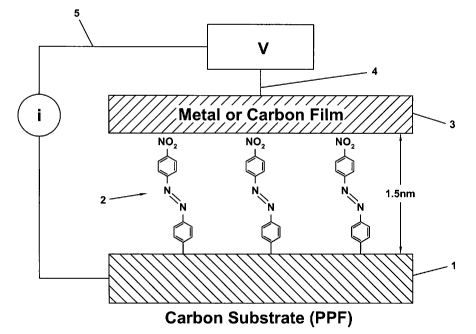
Figure 2 shows a schematic of a microelectronic junction in accordance with
another embodiment of the present invention. Figure 2 shows a first conductive
member 7 or substrate such as a carbon pyrolyzed photoresist film ("PPF"). To
this
first conductive member 7 is attached a single layer of a plurality of phenyl
pyridine
molecules (the "chemical monolayer"). The chemical monolayer 8 is disposed
between
the first conductive member 7 and the second conductive member 9 (i.e. a
conducting
metallic (or carbon) film), with a layer thickness as small as about 3
Angstroms.
The bonding of the conducting metallic (or carbon) film may be aided by
chemical
interactions between the metal and the monolayer 8, such as the Au:N
interaction where
gold is deposited onto phenyl pyridine molecules of the monolayer 8. The
resulting
structure accordingly may comprise two conductors separated by a molecular
monolayer that might have a variety of chemical structures and resulting
electrical
characteristics. The electrical and possibly optical properties of this
assembly depend on
tunneling or electrical conduction through the chemical monolayer. Since the
monolayer
may have a variety of chemical structures, its transfer function (i.e.,
current vs. voltage
response) may be varied greatly, from that of a pure dielectric to that of a
conductor,
with possibly important intermediate cases. The conduction mechanism may be
based
upon tunneling, Schottky emission, space charge-limited conduction, the Poole-
Frankel
effect, etc.
Figure 2 also shows electrical leads 10 and 11 that may be used to complete an
electrical circuit.
22
CA 02433887 2003-07-04
WO 02/063656 PCT/US01/49234
Figure 2 also shows an alternative molecular unit 12 (i.e. a diphenyl ethene
moiety) as an example of a molecular unit that may be bound to both the first
and
second conductive members, i.e., the PPF and a carbon film, respectively.
Naturally,
this type of arrangement may be obtained depending upon the chemical nature of
the
conductive members and the molecular unit(s) selected.
Figure 3 shows a schematic of the molecular orbitals (13, 14 and 15) of the
uncombined constituent portions of a molecular electronic junction similar to
that shown
in Figure 2. This Figure shows the uncombined molecular orbitals of the carbon
film 13,
a metal film 15 and an example of a chemical monolayer material 14 that is to
connect
them.
Figure 4 shows a schematic of the combined molecular orbitals of the carbon
PPF 13 and the chemically bonded organic monolayer 14 of a molecular
electronic
junction similar to that shown in Figure 2 with the exception that pyridyl
azobenzene is
shown as the molecular unit of the chemical monolayer. Figure 4 also shows the
orbital
arrangement of the uncombined metal film 14.
Figure 5 shows a schematic of the combined molecular orbitals of the carbon
PPF 13, the chemically bonded organic monolayer 14, and the metal film 15 of a
molecular electronic junction shown in Figure 4. This Figure shows that the
molecular
orbitals mix further with those of the metal, and that the electronic
properties of the
junction are determined by the molecular orbitals of the monolayer as modified
by the
bonding to the carbon and metal. This Figure also shows an external circuit
arrangement 16 to be completed by the electronic junction.
23
CA 02433887 2003-07-04
WO 02/063656 PCT/US01/49234
Figure 6 shows a plan view and cross-section insert of a photomicrograph of a
lithographically produced carbon film that may be used in accordance with one
embodiment of the invention. The PPF film 17 (e.g., a pyrolyzed AZ4330
photoresist) is
placed onto a silicon wafer 18. The photoresist may take any number of a wide
variety
of shapes or geometric arrangements so as to provide one or more regions that
may
permit the creation of one or more circuits. The monolayer 19 will be
positioned
between the patterned carbon film and a possibly correspondingly patterned top
contact
material, such as a metal contact layer 20. This may be used to produce an
array of
junctions that can be discreetly interrogated. In Figure 6, for instance, the
interdigitated
portions of the photoresist (on the right side of Figure 6) may be connected
by one or
more types of chemical monolayers to complete a circuit provided through the
electrical
lead portion of the photoresist (extending from the left side of Figure 6).
The
interdigitated portions of the photoresist in the displayed embodiment are
about 25 m
wide with 15 m gaps, although smaller features are possible in accordance
with the
application of known photoresist processes. The device shown in Figure 6 was
produced using a positive photoresist. However, similar structures may be
produced
using a negative photoresist.
Figure 7 shows a chemical sensor (i.e., a metal sensor) in accordance with
another embodiment of the present invention. Figure 7 shows PPF carbon film 21
and a
molecular unit 22 (of one or more type), a number of which that forms a
chemical
monolayer. The metal film 23 is also shown. Electrical leads 24 and 25
complete
external circuit 26. The presence of a chemical species such as a metal ion 27
(i.e.,
M2+) with which the molecular unit 22 is adapted to complex or bind, or by
which the
molecular unit(s) 22 otherwise may be electrically influenced. The presence of
the
metal ion or other species may in this way be ascertained and quantified as
desired.
24
CA 02433887 2006-11-14
Analogous devices may also be produced that may be sensitive to more than one
organic and/or inorganic species (discreetly or non-discreetly), such as being
sensitive
to ions per se or able to be sensitive to both magnesium and iron, for
instance.
Some of the relatively important characteristics of the preferred embodiment
include:
1. The pyrolyzed photoresist film (PPF) is very flat, about 5 Angstroms rms
roughness (Ranganathan et al. (2000).
2. The monolayer is bonded to the PPF surface covalently, and appears to be
quite
ordered. The bonding chemistry via diazonium ion reduction is well established
(Liu and
McCreery, 1995, Pinson, et al., 1992, Allongue, et al. 1991).
3. A small tunneling coefficient of 0.2 A'' is observed for an electron
tunneling
through the monolayer (Yang and McCreery, 1999) indicating unusual electronic
coupling between the PPF and the monolayer.
4. The monolayer thickness may be varied over a wide range by varying the
structure of the diazonium reagent.
Figures 8- 10 show a step-wise construction of a monolayer in accordance with
one embodiment of the present invention (i.e., showing the chemical monolayer
shown
in Figure 1). Figure 8 shows that a substrate such as glassy carbon or silicon
substrate
28. In this case, the width of the substrate 28 is approximately 1 cm while
the thickness
is approximately 3 mm. The substrate is a polished to a roughness of about
0.05
micrometers.
Figure 9 shows the substrate 28 is then provided with a positive photoresist
29
(i.e., AZ4330, commercially available from Hoechst Chemicals) to provide a
pyrolyzed
photoresist film 30.
CA 02433887 2003-07-04
WO 02/063656 PCT/US01/49234
Figure 10 shows a chemical method by which molecular units 31 may be
attached to the carbon PPF 32. This reaction causes the molecular units 31 to
be
conjugated to the pi orbital system. Typical coverage is on the order of 6 x
10"10 moles
per cm2. The molecular units 31 become preferentially oriented perpendicular
to the
surface of the carbon PPF 32.
Spectroscopic studies have shown that the Raman cross-section of the organic
monolayer is about 1000 times that in solution, and an electron tunneling rate
through
the chemical monolayer is approximately 105 faster than that for an aliphatic
(non-
conjugated) film.
Figure 11 shows model compounds of nitroazobenzene 33 bonded to the
graphite plane of the carbon PPF 34, and shows a graph of energy (eV) vs. the
number
of aromatic rings in the sp2 hybridized graphitic moiety. The graph shows that
the band
gap decreases from about 6 eV to about 3 eV when the graphite plane of the
carbon
PPF exceeds five rings. The modification of molecular orbital energies by
conjugation to
substrate permits the production of a molecular (i.e., organic) semiconductor.
In this
regard, the HOMO/LUMO gap is analogous to the band gap in semiconductors.
The ability to inject electrons into the LUMO allows for the production of
devices
based upon the ability of the electronic junctions of the present invention to
act as a
Schmidt trigger memory device. For instance, memory devices such as disk
drives,
flash memory cards, etc. may be created. These devices would operate by having
a
portion of the chemical monolayer excited through a relatively high potential
to inject
electrons into the LUMO where it may remain for a relatively long period of
time (i.e., on
the order of several minutes or hours). For instance, a disk drive may be
created using
a chemical monolayer in accordance with the present invention such that a read-
write
head could provide the required potential to selectively write, read and
rewrite to the
26
CA 02433887 2003-07-04
WO 02/063656 PCT/US01/49234
chemical monolayer segments that may be used as memory sectors. In similar
fashion,
the chemical monolayer of the present invention may be used as flash memory
segments. Because bistable memory switches may be made as small as a few
molecules in size, the potential data density may be very high in comparison
to known
memory devices. In this regard, one of the mechanisms by which a device of
this type
might operate is through the injections of electrons into the LUMO of the
chemical
monolayer.
Figure 12 shows a variety of types of organic molecular units that may be used
as components of the chemical monolayer of the present invention (shown here
extending from bases representing a substrate layer to which they are
chemically
bound). These may in turn be chemically bound to a second conductive layer or
otherwise placed into electrical contact with a second conductive component as
described above (not shown). They may also be used in a multiple-layer device
as
described above. It will be appreciated accordingly, that the chemical
structure may be
varied through a very wide range of molecule shape, functionality, band gap,
degree of
conjugation and size, and that the thickness of the monolayer may be varied as
well,
depending upon the size and shape of the molecular units.
Figure 13 shows an example of a multi-layer electronic device in accordance
with
one embodiment of the present invention. Figure 13 shows first conductive
component
35 comprising a first contact surface 36; a monolayer 37 of a first plurality
of
substantially parallel first molecular units having first and second ends,
each of the
parallel first molecular units of substantially the same length and attached
through its
first end to the first contact surface 36 through a conjugated bond; a second
conductive
component having first and second sides 39 and 40, respectively. The first
side 39 in
electrical contact with the second ends of the parallel first molecular units,
and the
27
CA 02433887 2006-11-14
second side 40 having a second contact surface; a monolayer 41 of a second
plurality of
substantially parallel second molecular units having first and second ends,
each of the
parallel second molecular units attached through their first end to the second
contact
surface of the second side 40 through a conjugated bond; and a third
conductive
component 42 having first and second sides 43 and 44, respectively. The first
side 43 is
in electrical contact with the second ends of the parallel second molecular
units. Figure
13 also shows that the monolayers 37 and 41 may become part of respective
electrical
circuits 45 and 46. Alternatively, multiple monolayer constructions of the
present
invention may be linked in a series to achieve accordingly different results
in an
electronic junction (i.e., taking advantage of the additive effects of each of
a series of
similar or dissimilar chemical monolayers).
Figures 14 and 15 show graphs of the current/voltage characteristics taken
from
experiments conducted on a monolayer described in Figures 1A and 1 B,, Figure
14
demonstrates an exponential dependence of current on applied voltage, which is
observed at low applied voltage (below about 1 volt). Figure 15 shows an
example of
"breakdown", in which the current suddenly increases at sufficiently high
voltage (-1.2
volts in this case).
Figure 16 shows a graph of the current/voltage characteristics taken from
experiments conducted on a monolayer described in Figures1A and 1 Bwhen
breakdown
is avoided. Figure 16 shows a bipolar current/voltage curve showing the
decrease in
apparent resistance at both positive and negative potentials. Figure 17 shows
a graph
of a current/time plot taken from experiments conducted on a monolayer
described in
Figures 1A and 1 B,, Figure 17 demonstrates the long-term stability of a
molecular junction
during cycling between +1.5 and -1.5 volts. Only minor changes in current
voltage
behavior occurred over 100,000 cycles during 14 hours.
28
CA 02433887 2006-11-14
Figure 18 shows a graph of the current/voltage characteristics taken from
experiments conducted on a monolayer described in Figures 1A and 1 B,,i=igure
19
shows a graph of the natural log of current vs. V'/'2 taken from experiments
conducted
on a monolayer described in FigureslA and 1 B. Figure 18 is the basis of
Figure 19,
which is a plot of the natural logarithm of the current vs. the square root of
the voltage.
The linearity demonstrated in Figure 19 is a strong indication that Schottky
emission is
the dominant mechanism of electron transport through the monolayer film.
Figure 20 shows a schematic of a memory device in accordance with one
embodiment of the present invention. Figure 20 shows memory device comprising
a
rigid support 47 (e.g., a rotating disk); a substrate (i.e., deposited PPF
substrate 48)
disposed on the rigid support and having a contact surface; and a monolayer 49
of a
plurality of substantially parallel molecular units having first and second
ends, and
attached through their first ends to the contact surface through a conjugated
bond, and
the second ends defining a scan surface. The molecular units are adapted to be
changed between a first memory state and a second memory state. At least one
read-
write device 50 is/are adapted to move along the scan surface of the monolayer
and
adapted to stimulate a change of the molecular units between the first and
second
memory states, and to determine the memory state status of regions on the scan
surface.
Figure 21 shows a schematic of a field emitter device in accordance with one
embodiment of the present invention. Figure 21 shows field emitter device 51
comprising a planar rigid support 52; a substrate disposed on the rigid
support and
having a contact surface and defining a plurality of extensions 53 extending
from the
rigid support; and a monolayer 54 of plurality of substantially parallel
molecular units
having first and second ends, and attached through their first ends to the
contact
29
CA 02433887 2003-07-04
WO 02/063656 PCT/US01/49234
surface through a conjugated bond, and the second ends defining an emission
surface,
the molecular units adapted to emit electrons in response to an applied
potential. The
device also includes a source of an applied potential adapted to stimulate the
molecular
units to emit electrons, and a planar emitter material 55 (e.g., a
fluorophore) disposed
facing the plurality of extensions and comprising a material adapted to emit
light upon
stimulation by incident electrons.
The present invention also includes methods of making chemical monolayers and
electronic junctions.
The method of producing a chemical monolayer construction comprises providing
a
substrate (preferably conductive carbon) having a contact surface; and
reacting a
chemical precursor bearing molecular units with the substrate so as to form a
monolayer
of a plurality of substantially parallel molecular units attached to the
contact surface of
the substrate, wherein the molecular units are attached to the substrate so as
to be
strongly coupled electronically to the substrate and wherein the molecular
units have an
average length, the contact surface of the substrate has a roughness value
that is
substantially less than or equal to the average length of the molecular units.
It is
preferred that the molecular units become attached to the substrate through a
conjugated bond.
CA 02433887 2003-07-04
WO 02/063656 PCT/US01/49234
The method of constructing an electronic junction comprises (a) providing a
first
conductive component, the first conductive component comprising: (i) a
substrate
having a contact surface; and (ii) a monolayer of plurality of substantially
parallel
molecular units having first and second ends, and attached through their first
ends to the
contact surface through a conjugated bond; and (b) placing a second conductive
component in electrical contact with the second ends of the substantially
parallel
molecular units. It is preferred that the second conductive component is
chemically
bound to the second ends of the substantially parallel molecular units. It is
also
preferred that the second conductive component is covalently bound to the
second ends
of the substantially parallel molecular units.
Industrial Applicability
The present invention may be used in the following industrial and commercial
applications:
1. Microelectronics
The existing microelectronics industry is based on semiconductors, such as
silicon and metal oxides, fabricated into a variety of junctions between
semiconductors
to make P/N junctions, diodes, transistors, etc. The monolayer junction
disclosed herein
may have quite different and more versatile properties than conventional
semiconductor
junctions. Since the molecular orbitals of the monolayer can be varied by
alterations in
chemical structure, a wide variety of transfer functions is possible. PPF or
similar
smooth substrates may be fabricated in complex patterns via photolithography,
so it
may be possible to combine monolayer junctions with conventional semiconductor
microcircuits. Possible new microdevices based on monolayer junctions include
capacitors, multistate storage elements, and optically sensitive switches. It
is possible
31
CA 02433887 2003-07-04
WO 02/063656 PCT/US01/49234
that molecular electronic junctions may consume much less power than
conventional
electronic circuits, increasing portability and decreasing heat output.
2. Photodetectors and Imaging Devices.
The monolayer may be made photosensitive, by choosing a molecule with a
HOMO/LUMO gap corresponding to the desired photon energy. A thin metallic
layer
would be partially transparent, and photon arrival at the monolayer would
trigger a
conductivity increase, similar to a photodiode. Since the HOMO/LUMO gap is
variable,
the device could be made to be wavelength specific. An array of such junctions
could
serve as an image collector, with color resolution made possible by the
creation of multi-
color-capable pixels. In addition, photodetectors might be combined with fiber
optic and
photonic circuits to yield a fast optical/electrical transducer.
3. Chemical Sensors
The molecular orbitals of the monolayer molecule may be sensitive to the
chemical environment. For example, a bipyridyl spacer (Figure 7) interacts
with metal
ions, and might yield a change in conductivity. A pattern of junctions would
be required,
since access to the monolayer is at its edge. Analysis of gases, liquids and
solutions is
amenable to this approach, with possible applications in clinical analysis,
environmental
monitoring, and process analytical chemistry.
4. Light Emission
By analogy to light emitting diodes, a potential across the proposed monolayer
junction should inject elections into a high-energy orbital of the monolayer.
The electron
may then make a transition to a lower energy orbital, emitting light. Arrays
of such
devices could be used in flat-panel displays or surface emitting diode arrays,
with color
controlled by the energy levels of the monolayer. Extension of light emission
to
amplification and lasing are conceivable.
32
CA 02433887 2003-07-04
WO 02/063656 PCT/US01/49234
5. Voltage Modulation of Reflectivity
For a thin metallic overcoat, the optical properties of the metal surface may
depend on both the identities of the monolayer and the applied potential. The
reflectivity
vs. wavelength curve of the metal may be voltage dependent, and possibly
modulatable
on a rapid time scale. Color video projection and panel displays using natural
or
artificial white light are also possible.
Other applications of the monolayer junction to the microelectronics,
photonics,
and display industries, may become apparent to one skilled in these arts. The
versatility
inherent in a device, which exploits a molecule as a circuit element, may be
as important
an advance as the semiconductor junctions that spawned all of modern
electronics.
References:
1. C.A. Mirkin, M.A. Ratner, "Molecular Electronics", Annu. Rev. Phys. Chem.,
1992,
43, 719 - 754.
2. M.A. Reed, J.M. Tour, "Computing with Molecules", Scientific American,
2000,
86-93
3. L.A. Bumm, J.J. Arnold, M.T. Cygan, T.D. Dunbar, T.P. Burgin, L. Jones,
D.L.
Allara, J.M. Tour, P.S. Weiss, "Are single Molecular Wires Conducting?",
Science, 1996, 271, 1705
4. C. Zhou, M.R. Deshpande, M.A. Reed, L. Jones, J.M. Tour, "Nanoscale
Metal/Self-Assembled Monolayer/Metal Heterostructures", Appl. Phys. Left.,
1997, 71(5), 661.
5. M.A. Reed, C. Zhou, C.J. Muller, T.P. Burgin, J.M. Tour, "Conductance of a
Molecular Junction", Science, 1997, 278, 252.
6. L.A. Bumm, J.J. Arnold, T.D. Dunbar, D.L. Allara, P.S. Weiss, "Electron
Transfer
through Organic Molecules", J. Phys. Chem. B., 1999, 103, 8122-8127.
7. C.P. Collier, E.W. Wong, M. Belohradsky, F.M. Raymo, J.F. Stoddart, P.J.
Kuekes, R.S. Williams, J.R. Heath, "Electronically Configurable Molecular-
Based
Logic Gates", Science, 1999, 285, 391 -393
8. C.P. Collier, G. Mattersteig, E.W. Wong, Y. Luo, K. Beverly, J. Sampaio,
F.M.
Raymo, J.F. Stoddart, J.R. Heath, "A [2]Catenane-Based Solid State
Electronically Reconfigurable Switch", Science, 2000, 289, 1172 - 1175.
33
CA 02433887 2006-11-14
9. J. Pinson, J. Saveant, R. Hitmi, "Process for Modifying the Surface of
Carbon-
Containing Materials by Electro-Chemical Reduction of Diazonium Salts,
Applicable in Particular to Carbon Fibers For Composite Materials: Carbon-
Containing Materials So Modified", French Patent, PCT/FR92/0087, 1992.
10. P. Allongue, M. Delamar, B. Desbat, O. Fagebaume, R. Hitmi, J. Pinson,
J.M.
Saveant, "Covalent Modification of Carbon Surfaces by Aryl Radicals Generated
from the Electrochemical Reduction of Diazonium Salts", J. Am. Chem. Soc.,
1997, 119, 201-207
11. Y-C. Liu, R.L. McCreery, "Reactions of Organic Monolayers on Carbon
Surfaces
Observed with Unenhanced Raman Spectroscopy", J. Am. Chem. Soc., 1995,
117, 11254.
12. S. Ranganathan, R. McCreery, S.M. Majji, M. Madou, "Photoresist-Derived
Carbon for Microelectrochemical Applications", J. Electrochem. Soc., 2000.
147,
277 - 282.
The preferred embodiments herein disclosed are not intended to be exhaustive
or
to unnecessarily limit the scope of the invention. The preferred embodiments
were
chosen and described in order to explain the principles of the present
invention so that
others skilled in the art may practice the invention. Having shown and
described
preferred embodiments of the present invention, it will be within the ability
of one of
ordinary skill in the art to make alterations or modifications to the present
invention, such
as through the substitution of equivalent materials or structural
arrangements, or
through the use of equivalent process steps, so as to be able to practice the
present
invention without departing from its spirit as reflected in the appended
claims.
It is the intention,
therefore, to limit the invention only as indicated by the scope of the claims
and
equivalents thereof.
34