Note: Descriptions are shown in the official language in which they were submitted.
CA 02434091 2007-07-18
1
Radiation Detector Comprising a Hybrid Perovskite
Scintillator
Technical field of the invention
This invention relates to a radiation detector for ionizing
radiations, such as y-rays, X-rays, electron beams, heavy charged
particle beams and neutron beams, and more specifically, having a
very short time from a rise to a disappearance of luminescence of
subnanosecond order.
Prior art
A scintillator detects and measures ionizing radiation
optically by using a solid radiation relaxation phenomenon. In
recent years, in fields such as physics, chemistry, biology and
medicine, the use of short-pulsed radiation is becoming more
widespread and simple methods of measuring short-pulsed radiation
are required. For example, in the case of a PET (positron emission
tomography) which is a medical device, the time resolution of the
scintillator is directly linked to the spatial resolving power of
the system, so the higher the resolving power of the scintillator
is, the more precise the diagnosis that can be performed. There
is therefore a demand for a high resolving power scintillator.
Scintillators may use organic crystals such as anthracene,
inorganic crystals such as sodium iodide doped with thallium, or
ceramics such as PWO which have recently been developed, but even
those with a fast luminescence decay time constant are only of
nanosecond order. Among scintillators in practical use, barium
fluoride is unique in having a decay time constant (600 picoseconds)
of subnanosecond order (M.Laval, M.Moszynski, R.Allemand,
E.Cormoreche, P.Guinet, R.Odru and J.Vacher, Nucl.Instru.Meth.,
206 (1983) 169), but as its luminescence wavelength is in the
ultraviolet region, there are severe practical restrictions to its
use. Such inorganic scintillators can roughly be classified into
CA 02434091 2003-07-02
2 FS02-277
two groups. The first group have a large luminescence quantum
efficiency but a slow time constant of 200 nanoseconds or more
(NaI(T1), CsI(Tl), CsI(Na), BGO, CdWO9), and the other group has
a small luminescence quantum efficiency and a fast time constant
of 1 to 30 nanoseconds (BaF2, CsF, CeF31 CsI, organic scintillators) .
For example, GSO (Ce) has an intermediate luminescence intensity and
an intermediate time constant (60nanoseconds), but its performance
does not satisfy practical requirements (Carel W.E van Eijk,
"Nuclear Instruments & Method in Physics Research Section A -
Accelerators Spectrometers Setectors and Associated Equipment"
Nucl.Instr.and Meth.A 392 :(1-3)285-290 JUN 21 1997, 460 :(1)1-
14 MAR 11 2001).
Thus, an ideal scintillator has not yet been discovered, but
the search for a material having a high luminescence intensity and
a short time constant is continuing.
Problems to be solved by the invention
The Inventors already proposed a radiation detector using a
two-dimensional stratified compound (R-NH3) 2MX4 as an
organic/inorganic hybrid compound scintillator (Japanese Patent
Application No. 2001-006132) . This compound has an exciton with a
very large bound energy in a self-organized quantum well structure.
Its decay time constant is approx. 100 picoseconds, and of the
scintillators which have so far been reported, it is therefore one
of the substances with the shortest time from rise to disappearance
of luminescence. However, as its crystallizing ability is low
compared with inorganic crystals or ceramics, it is difficult to
produce crystals having a large volume. Therefore, for detecting
a high LET radiation pulse such as a heavy charged particle,
sufficient scintillation efficiency can be obtained even with a
spin coat film, but for detecting a low LET radiation pulse such
as a y-ray and high-speed electron beam, it has the disadvantage
CA 02434091 2003-07-02
3 Fs02-277
that its scintillation efficiency falls as the LET (linear energy
transfer) decreases.
Means to solve the Problems
This invention solves the above-mentioned problem, and
provides a radiation detector using a scintillator having a large
luminescence intensity and a short time constant.
Specifically, the Inventors discovered that when three-
dimensional perovskite organic/inorganic hybrid compounds
represented by the general formula AMX3 (wherein, A, M, X are as
described later) were excited by an ionizing radiation, intense
radiation accompanied the relaxation step, this scintillation
luminescence had a single peak in the visible region, and although
the time from rise to disappearance of this luminescence was longer
than in the case of the two-dimensional stratified compound (R-
NH3)ZMX9, it was shorter than in the case of other ordinary
scintillators.
Further, the Inventors succeeded in growing good quality,
high volume crystals of this three-dimensional compound from a
solution thereof, and discovered that in a test where it was
irradiated with a short pulse electron beam, the radiation
relaxation step was a high-speed exciton luminescence of
subnanosecond order.
As the three-dimensional compound AMX3 (wherein, A, M, X are
as described later) does not have a multi-layer structure
comprising an inorganic layer and organic layer as in the case of
the two-dimensional compound (R-NH3) 2MX4, the exciton bound energy
is low (in the former case, approx. 40meV, and in the latter case,
approx. 300meV), however an exciton luminescence having a peak
wavelength of 550nm at room temperature was still observed.
This three-dimensional compound forms a three-dimensional
network wherein clusters comprising six halogens X coordinated to
CA 02434091 2007-07-18
4
a divalent metal are shared, so compared with the two-dimensional
stratified compound (R-NH3)ZMXõ the crystallizing ability is high.
Therefore, crystals of large volume can easily be obtained, and an
improvement of scintillation efficiency for low LET radiation can
be realized.
In view of the characteristics of this three-dimensional
compound, the compound, and in particular its crystals, can be
widely used as a high-speed response scintillator for ordinary
ionizing radiations. On the other hand, the two-dimensional
stratified compound (R-NH3) 2MX, may be used for special cases as an
ultra high-speed scintillator for very short super-single pulsed
radiations, or as a scintillator for the simple detection of high
LET radiations by a spin coat film of this compound. Therefore,
these two compounds may be used in different situations according
to the application.
In particular, crystals of the three-dimensional compound of
this invention allow the detection of low LET radiations such as
y-rays and X-rays, which was difficult using the two-dimensional
stratified compound of the prior art, and offer a higher time
resolution than that provided by ordinary scintillators such as
other inorganic crystals, organic crystals or ceramics.
Specifically,. this invention is a radiation detector
comprising as a scintillator an organic/inorganic perovskite
hybrid compound represented by the general formula AMX3, wherein
A is R-NH3 or R'=NH2, or a mixture thereof, R is a hydrogen atom
or a methyl group which may be substituted by an amino group or a
halogen atom, R' is a methylene group which may be substituted by
an amino group or a halogen atom, each X is a halogen atom that may
be identical to or different from the other X groups, and M is a
Group IVa metal, Eu, Cd,Cu, Fe, Mn or Pd. An example of this
perovskite organic/inorganic hybrid compound where A is a mixture,
is (CH3NH3) ~1_x~ (NH2CH=NH2),PbBr3 (0<x<1) . This radiation detector is
CA 02434091 2003-07-02
FS02-277
suited to detect low LET radiation, and in particular the low LET
radiation is a pulse.
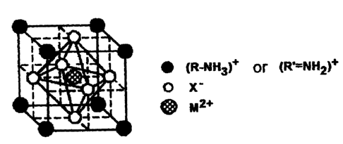
Brief Description of the Drawings,
5 Fig. 1 shows the basic structure of an organic/inorganic
perovskite hybrid compound according to this invention.
Fig. 2 shows a schematic view of a device for manufacturing
single crystals of the perovskite compound by the poor solvent
diffusion method. A is a glass bottle into which the perovskite
compound is introduced, B is a glass bottle into which a poor solvent
is introduced, and C is a desiccator.
Fig. 3 shows a schematic view of a device which excites single
crystals of PbBr (CH3NH3) 3 using the electron beam pulse of a linear
accelerator (LINAC), and allows observation of the luminescence.
Fig. 4 shows the time profile of the scintillation of
PbX ( CH3NH3 ) 3 .
Fig. 5 shows the temperature dependency of the luminescence
intensity (ultraviolet irradiation) of single crystals of the
perovskite compound.
Fig. 6 shows a device showing that single crystals of the
perovskite compound can detect y-rays.
Fig. 7 shows the scintillation emission spectrum when single
crystals of the perovskite compound are irradiated by y-rays.
Detailed description of the invention
In the scintillator of this invention represented by MX3
(wherein, A is R-NH3 or R'=NH2, or a mixture thereof), A is a
monovalent cation with a small volume such as [CH3NH3]+ or [NH4]+.
The two-dimensional organic/inorganic perovskite hybrid compound
(R-NH3) 2MX4 of the prior art uses an alkyl group (C,H2,+1) wherein n
is for example 2-18, as the hydrocarbon group R, and it has a
multi-layer structure wherein inorganic layers formed by
CA 02434091 2003-07-02
6 FS02-277
octahedronal clusters of a lead halide are separated by an organic
material. However, in this invention, the volume of (R-NH3) or
(R'=NH2) is less than the volume of lead halide clusters, so the
inorganic layers are not separated by the organic material, an
inorganic three-dimensional network is formed, and the organic
material instead penetrates the gaps in the octahedronal clusters
of metal halide. The basic structure at room temperature is shown
in Fig. 1. Fig. 1 shows how the organic material represented by
(R-NH3) or (R'=NH2), is occluded in the spaces between the metal
(e.g., lead) halide of this invention.
The detector of this invention comprises a scintillator and
a light-receiving device, a three-dimensional perovskite compound
being used as the scintillator.
The three-dimensional perovskite compound used in this
invention is the compound represented by the general formula AMX3,
where A is is R-NH3 or R'=NH2, or a mixture thereof.
Herein, the conditions regarding (R-NH3) or (R'=NH2) are that
they should be monovalent cations of such a size that they can be
occluded within the aforesaid three-dimensional compound.
Specifically, R is methyl or hydrogen, and this methyl group may
be substituted by an amino group or halogen atom. R' represents
a methylene group, and this methylene group may be substituted by
an amino group or halogen atom. Examples of this (R-NH3) or (R'=NHZ)
are H-NH3, CH3-NH3 and NH2CH=NH2 (formamidinium cation) . However,
in the case of C2H5-NH3, the product is a two-dimensional stratified
compound (Japanese Unexamined Patent Application No.2001-006132),
and not the three-dimensional compound of this invention.
X in the aforesaid general formula represents a halogen atom,
preferably Cl, Br or I. From the viewpoint of stability of the
compound, Br is most preferred, but from the viewpoint of low LET
radiation detection, I which has a large atomic number is most
preferred. Also, X may be a mixture of these halogens. M is a Group
CA 02434091 2003-07-02
7 FS02-277
IVa metal, Eu, Cd, Cu, Fe, Mn or Pd, preferably a Group IVa metal
or Eu, more preferably a Group IVa metal, still more preferably Ge,
Sn or Pb, and most preferably Pb.
This scintillator is preferably a single crystal described
hereafter, but it is not necessarily a single crystal, and may be
a polycrystal for example coated by spin coating or the like on a
solid substrate. This solid substrate must not emit luminescence
which would interfere with measurements, therefore silicon
crystals may for example be used.
As this scintillator emits light in the visible region, a
photomultiplier or the like may be used as the light-receiving
device. Typical examples are a construction wherein the
scintillator is in contact with the light-receiving surface of the
photomultiplier, a construction wherein the scintillator and the
photomultiplier are connected by a light waveguide such as an
optical fiber or the like, and a construction wherein the light
emitted by the scintillator is received by a light-receiving port
separated from the sciritillator, this light-receiving port being
connected to the photomultiplier by a light waveguide. The signal
from the light-receiving device is processed by the usual method.
The scintillator in the radiation detector of this invention
has a high crystal-forming ability, and single crystals of large
volume can be formed. Therefore, the high-speed exciton
luminescence can be applied not only to the detection of high LET
radiation beams such as a-rays and heavy charged particle beams,
but also to the detection of low LET radiation beams such as y
-rays, X-rays and high-speed electron beams. Further, it may also
easily be applied to the detection of short pulses of low LET
radiation beams which were difficult to detect in the prior art.
The radiation detector using the three-dimensional
perovskite compound of this invention, e.g., (CH3NH3) PbX31 has the
following characteristics.
CA 02434091 2003-07-02
8 FS02-277
As the scintillator, i.e., the perovskite organic/inorganic
hybrid compound of this invention, has an increased luminescence
intensity the lower the temperature is, it is preferred to cool the
measurement system.
The scintillator is easily manufactured. When the
organic/inorganic hybrid compound deposits from an organic
solution, a three-dimensional network of self-organizing lead
halide clusters is formed, so it can be very economically mass-
produced without requiring high temperature or high pressure as in
the case or inorganic crystals or ceramic scintillators.
As the exciton luminescence peak of the organic/inorganic
hybrid compound is unique (e. g., in the case of (CH3NH3) PbBr3, 550nm) ,
the measurement system can be simply constructed from a light
waveguide and light-receiving device alone.
Hereafter, this invention will be described by means of
specific embodiments, but the invention is not to be construed as
being limited in any way thereby.
Example 1
60.22g hydrobromic acid (HBr, Wako Pure Chemicals,
concentration 0.48) was introduced in a 200ml flask at room
temperature, and 27.06g of 40% aqueous methylamine solution (Wako
Pure Chemicals, concentration 0.41) was gradually dripped in. As
this is an exothermic reaction, the flask was placed in a water bath.
Methylamine was dripped until the molar ratio of hydrobromic acid,
HBr, to methylamine, CH3NH21 was 1: 1. After addition was complete,
the mixture was left with stirring for 1 hour to complete the
reaction, and a colorless, transparent aqueous solution of
methylamine bromide was thus obtained. When water was removed on
an evaporator (water bath temperature 45 C), a white powder of
methylamine bromide remained. This was washed by diethyl ether
CA 02434091 2007-07-18
9
(suctionfiltration), and after removing unreacted material, it was
dried. The yield was 35.98g, i.e., 90.0%.
Next, 18.8g of the methylamine bromide obtained as mentioned
above was dissolved in 100m1 DMF in a 200m1 three-necked flask at
room temperature, and 61.62g lead bromide, PbBr2 (Highly Pure
Chemicals, purity 99.99%) was added a little at a time until the
molar ratio of methylamine bromide and lead bromide, PbBr21 was 1: 1.
To avoid reaction between the moisture in the air in the three-
.necked flask, the mixture was left with stirring for 1 Yiour.to
complete the reaction while steadily passing a current of dry
nitrogen through the flask, and a DMF solution (transparent and
colorless) of the perovskite type compound, (CH3NH3)PbBr3, was
thereby obtained. The solvent was evaporated on an evaporator
(water bath temperature approx. 80 C), and a microcrystalline
powder of a red perovskite compound remained. This was washed by
diethyl ether to remove unreacted material, and dried. The yield
was 78.41g, i.e., 97.5%.
Next, a single crystal of the perovskite compound used as the
scintillator was prepared by the poor solvent diffusion method
using the device shown schematically in Fig. 2 (Reimei Hirayama,
"Organic Crystal Manufacturing Handbook", Chapter 8, "The
Crystallization of Organometal Complexes", 2001, Maruzen
Publishing Co.).
The microcrystalline powder of the obtained perovskite
compound was diSsolved in as little of a good solvent (dehydrated
DMF) as possible, and undissolved material was filtered off using
a filter having a retention capacity of about 0.1 micrometers
(MILLIPORE,M Millex-LG SLLGH25NB). This solution was introduced
into a container (glass bottle A) for depositing crystals. Glass
bottle A was subjected to ultrasonic cleaning with pure water
beforehand. Next, a poor solvent (toluene, diethyl ether,
nitromethane, etc.) was introduced into a glass bottle B. In order
CA 02434091 2003-07-02
FS02-277
to dehydrate the poor solvent, a little calcium chloride powder was
also introduced into glass bottle B. Glass bottle A and glass bottle
B were stored in a desiccator, sealed off from the atmosphere, and
left for four days at room temperature. At this time, the poor
5 solvent which evaporated from glass bottle B spread into the
perovskite compound solution in glass bottle A so that the
solubility of the solution in glass bottle A gradually fell, and
red, transparent single crystals of perovskite type compound
deposited on the bottom of glass bottle A. Glass bottle A was shaded
10 by wrapping the whole desiccator in aluminum foil. Of the single
crystals thus obtained, those with the largest volume measured
lcmxlcmx5cm.
When the obtained single crystals were excited using an
electron beam pulse of 200 femtoseconds accelerated to 30MeV by a
linear accelerator (LINAC) in vacuo (approx. 10-6 torr), a
luminescence with a peak wavelength of 550nm was observed.
The time transition of luminescence intensity of this luminescence
was measured using a streak camera (Hamamatsu Photonics, Inc.,
FESCA-200) with a resolving time of 260 femtoseconds as light-
receiving device. This device is shown schematically in Fig. 3,
and the result is shown in Fig. 4. As a result of this numerical
analysis, the decay time constant of this luminescence was approx.
240 picoseconds.
Examnle 2
While varying the temperature of the single crystals
manufactured in Example 1, a scintillation luminescence spectrum
from the sample was measured by irradiating it with hydrogen ions
of 2. OMeV using a Van der Graaf accelerator (Tokyo University Atomic
Energy Research Center). The measurement result showed an
identical relation to the relation between luminescence intensity
due to irradiation with ultraviolet light (He-Cd laser), and
CA 02434091 2003-07-02
11 FS02-277
temperature.
The result of irradiation with ultraviolet light is shown in
Fig. S. Taking the reference value of luminescence intensity for
NaI (Tl) as 100, the luminescence intensity of this compound at 300K
was 0. 075, and at 25K was 140. The luminescence intensity decreases
exponentially as a function of the absolute temperature.
Examr)le 3
In this example, the single crystal manufactured in Example
1 was irradiated with y -rays, and it was confirmed that this single
crystal could detect the y-rays.
A schematic view of the system used in this test is shown in
Fig. 6. 22Na was the sealed source of the y-rays, and the intensity
was 370Bq (Becquerels) . The single crystal was sealed in a cryostat
cold finger, and cooled to 40K. The luminescence was directly
received by a PMT (photomultiplier, Phillips, XP4222B) attached to
a quartz glass window. The signal from the PMT was amplified by
an AMP, and recorded as an energy spectrum by an MCA (wave height
discrimination machine). The result is shown in Fig. 7.
In Fig. 7, the solid line shows the signal intensity when the
single crystal was installed and cooled to 40K. On the other hand,
the black shaded part shows the noise level for the signal intensity
when there is no scintillator crystal. From the difference, it can
be seen that the single crystal emits a scintillation luminescence
when y-rays are received.