Note: Descriptions are shown in the official language in which they were submitted.
CA 02434108 2003-06-30
US-version / RAI
Patent-Treuhand-Gesellschaf t
fur elektrische Gliihla~npen mbH. , N~un:ich
Title
Drive for a half-bridge inverter
Technical field
The invention proceeds from a half-bridge inverter with
the following features:
~ The half-bridge inverter is connected to a
positive pole and a negative pole of a power
supply.
~ an upper and a lower half-bridge switch (T1, T2)
that respectively have a control input, a working
electrode and a reference electrode, the upper
half-bridge switch being coupled with its working
electrode to the positive pole , and the lower
half-bridge switch being coupled with its
reference electrode to the negative pole ,
~ a control module that outputs at a <control output
a rectangular control signal that can have a low
state and a high state, and
~ a level shift switch that is coupled to the
negative pole and is controlled by the control
module
The invention relates to the generation of an optimal
dead time in which none of two half-'.bridge switches may
be switched on.
Background art
Half-bridge inverters are sufficiently well known for
generating an ac voltage from a do voltage. They are
widely used in switched-mode power: supplies (SMPS).
Since the half-bridge inverter is cost effective with
reference to other switched-mode power supply
CA 02434108 2003-06-30
- 2 -
topologies (for example full-bridge inverters), i.t is
dominant, in particular, in cost-sensitive areas such
as lighting engineering. Electronic operating units for
fluorescent lamps or halogen incandescent lamps are
virtually exclusively equipped with half-bridge
inverters.
A half-bridge inverter essentially cc>mprises the series
circuit of an upper and a lower half-bridge switch that
is connected to a power supply that essentially
constitutes a do voltage with a positive pole and a
negative pole. This is a rectified line voltage in the
simplest case. Provided at the tie point of the
half-bridge switches is a half-bridge output voltage
UHB which has a substantial ac voltage component and
feeds a load circuit that picks a load current IL. In
the case of lighting engineering, the load circuit
essentially comprises a reactance nE=twork with one or
more lamps as energy consumers.
In general, two half-bridge switches are designed as
electronic switches such as, for example, MOSFET,
bipolar transistor or IGBT. For technical reasons
relating to semiconductors, it is mostly N channel or
NPN transistors that are used in power electronics, for
which reason the following statements deal with this
type of transistor. However, it is also possible
throughout to use transistors complementary thereto.
All that need be done is to invert the polarity of the
power supply and, where appropriate, the drive of the
transistors. In the case of N-channel or
NPN-transistors, the upper half-bridge switch is
coupled to the positive pole, and the lower transistor
is coupled to the negative pole, the negative pole
constituting a reference potential for the entire
circuit arrangement including the half-bridge inverter.
This also explains the designations of upper and lower
half-bridge switch: the upper half-bridge switch is at
a higher potential than the lower half-bridge switch in
CA 02434108 2003-06-30
- 3 -
relation to the reference potential, at least during
the time it is switched on.
It must be avoided in any case that the two half-bridge
switches are switched on simultaneously, since
otherwise the power supply is short circuited. However,
there is inserted between the phases in which one of
the two half-bridge switches is switched on a phase in
which none of the two half-bridge switches is switched
on. This phase is termed dead time in the literature.
The dead time has the function not only of creating a
safety gap between the switched-on phases of the
half-bridge switches, but rather the: tie point of the
half-bridge switches is to be given the opportunity to
change its potential during the dead time. The energy
that is stored in the load circuit, and largely in
inductive components there, is capable o. eliminating,
or at least minimizing, the voltage at the half-bridge
switch that is switched on after the dead time.
Consequently, the relevant half-bridge switch can be
switched on without losses or at least with the minimum
possible loss. This state of affairs is also denoted in
the literature as zero voltage switching (ZVS). The
time that passes until the tie point of the half-bridge
switches has assumed a potential that ensures minimal
switch-on losses is denoted below as the reversal time.
The electronic switches used as half-bridge switches
generally have a working electrode (for example drain,
collector), a reference electrode (for example source,
emitter) and a control electrode (for example gate,
base). The control electrode forms a control input of
the half-bridge switch. The switch is generally
switched on by a drive signal that is present between
the control electrode and reference electrode. Figure 1
illustrates a prior art relating to how the drive
signals are provided for the half-bridge switches.
CA 02434108 2003-06-30
- 4 -
The half-bridge switches T1 and T2 are designed as
MOSFETs in figure 1. The upper half-bridge switch T1 is
connected in series with the lower half-bridge switch
T2. The drain terminal of the upper half-bridge switch
T1 is connected to the tie point J3, to which the
positive pole of the power supply is connected. The
source terminal of the lower_ half-bridge switch T2 is
connected to the tie point J1, to which the negative
pole of the power supply is connected. As may be seen
from figure 1, the potential of J1 forms a reference
potential for the half-bridge inverter. shown. The
source terminal of T1 and the drain terminal of T2 are
connected and are fed to the tie point J2 that forms
the half-bridge output. At J2, the half-bridge inverter
supplies a half-bridge output voltage UHB to a load
circuit. The driving of the gate terminals of T1 and T2
is described below as it correspond; to the prior art
and is illustrated in figure 1.
A control module 1 that is supplied with energy via the
tie point J4 of an auxiliary voltage supply makes a
rectangular control signal available at:, its control
output 2. The form of the control signal corresponds to
the inverse of the desired form of the half-bridge
output voltage UHB. The control signal can assume a low
state and a high state. The intention is that the upper
half-bridge switch T1 is switched on in the low state
of the control signal, and the lower half-bridge switch
T2 is switched on in the high state. The control signal
is connected to the gate of the lower half-bridge
switch T2 via the parallel circuit of a resistor R1 and
a diode D1. Consequently, the voltage value of the
control signal in a high state must be at least as
great as the gate/source voltage that is required for
switching on the lower half-bridge switch T2. The
voltage value of the control signal in the low state
must be lower than the minimum value that is required
for the relevant gate/source voltage for switching on.
The resistor R1 effects a switching-on delay for T2
CA 02434108 2003-06-30
- 5 -
that is bridged by the diode D1 in order to switch off
T2.
Providing the drive signal for the upper half-bridge
transistor Tl is more complicated, since the reference
electrode of T1 is not at the same potential as the
reference potential of the control module. In
accordance with figure 1, an upper drive circuit 3 is
provided for the upper half-bridge transistor T3. In
the simplest case, this drive circuit comprises a totem
pole circuit known from the literature. The output of
the upper drive circuit is connected to the gate of the
upper half-bridge transistor T1. The energy for the
upper drive circuit is fed via the terminals 4 and 5,
the terminal 5 also constituting the reference
potential for the output of the upper drive circuit,
and an operating voltage of the upper drive circuit
being required at the terminal 4. The energy supply for
the upper drive circuit is implemented by a known pump
circuit comprising the capacitor C1 and the diode D2.
C1 and D2 are connected in series between the auxiliary
voltage supply at the tie point J4 and tale half-bridge
output at the tie point J2. The energy for the upper
drive circuit is drawn from the capacitor C1.
The input of the upper drive circuit 6 is connected via
a pull up resistor R2 to the terminal 4 of the upper
drive circuit, at which the operating voltage thereof
is present. Without further measures, the pull up
resistor R2 is led to a control signal for an upper
half-bridge transistor that switches the latter on. It
is therefore necessary to ensure that the upper
half-bridge transistor T1 is switched off in the high
state of the control signal from the control module. A
level shift switch T3 fulfills this purpose. It is
designed in figure 1 as a MoSFET whose drain terminal
is connected to the input of the upper drive circuit 6,
whose gate terminal is connected to the control output
of the control module 2, and whose source terminal is
CA 02434108 2003-06-30
- 6 -
connected, via a current negative feedback resistor R3,
to the reference potential of the half-bridge inverter.
The level shift switch T3 is switched on in the high
state of the control signal, as a result of which the
voltage at the input of the upper drive circuit 6 is
reduced to a value that causes the upper half-bridge
transistor T1 to be switched off. The: draw terminal of
the level shift switch T3 is additionally connected to
the half-bridge output J2 via a diode D3. This prevents
a current from flowing through the upper drive circuit
when the level shift switch T3 is switched on. D3 is
preferably designed as a Schottky diode, in order to
keep low a forward voltage that occurs. The current
negative feedback resistor R.3 is intended, to limit the
current through the level shift switch T3.
In the case of the circuit described, a switching-on
delay of the upper half--bridge transistor Tl is
provided by virtue of the fact that the Miller
capacitance of T3 must be charged via R2 after T3 has
been switched off. The upper_ half-bridge transistor Tl
is not switched on until the voltage across this Miller
capacitance exceeds a given threshold value at the
input 6 of the upper drive circuit. Thus, the desired
dead time that passes between switching off the lower
half-bridge transistor T2 and switching on the upper
half-bridge transistor T1 can be set by the value of
the pull up resistor R2.
The switching-on delay for the lower half-bridge
transistor T2 cannot be implemented in this way. Only
the resistor Rl offers the possibility of modifying the
charging time of the gate/source capacitance of the
lower half-bridge transistor T2. However, it is
possible thereby to realize only dead times that are
shorter than the above named reversal time. Longer dead
times would cause the lower half-bridge transistor T2
to be operated too long in the so-called linear working
range in which very large losses occur.
CA 02434108 2003-06-30
Document US 5,550,436 (Houk) describes a dead time
generation for the transition from the upper to the
lower half-bridge transistor by means of a switching-on
delay unit (LSDELAY) for the lower half-bridge
transistor. However, this solution has two
disadvantages: firstly, the said switching-on delay
unit forms a part of an integrated circuit, and this
means a substantial outlay an costs; secondly the dead
time is fixed far a given dimensioning and does not
match the above named reversal time. Consequently, the
dead time must always be longer than the optimal dead
time, and this leads to losses in efficiency of the
half-bridge converter.
Disclosure of the invention
Tt is an object of the present invention to provide a
half-bridge inverter in accordance w_Lth the preamble of
claim 1 which provides an optimal dead time cost
effectively.
This object is achieved by means of a half-bridge
inverter having the features of the preamble of claim 1
by means of the features of the characterizing part of
claim 1. Particularly advantageous refinements are to
be found in the dependent claims.
According to the invention, the control input of the
lower half-bridge switch is coupled to the control
output of a control module via an interrupt initiation
switch. The high state of the control signal thereof
can therefore not lead directly to switching on the
lower half-bridge transistor. Rather, this first
requires the interrupt initiation switch to be switched
on. Thus, the switching on of the lower half-bridge
transistor can be delayed with the aid of the interrupt
initiation switch until the reversal time has elapsed.
CA 02434108 2003-06-30
An indicator that the reversal time has elapsed is
formed according to the invention by the current
through a level shift switch. If the control signal at
the control output of the control module goes over to
the high state, the level shift switch is firstly
switched on. Since at this instant the half-bridge
output is at the positive potential of the power
supply, there firstly flows through thE: level shift
switch a high current that is essentially limited by a
current negative feedback resistor. As long as this
current is above a prescribed threshold, the interrupt
initiation switch is switched off :in accordance with
the invention, and the lower half-bridge switch is not
driven. After the above described reversa=L operation of
the half-bridge, the potential of the half-bridge
output is at the potential of the reference potential,
or the negative pole. At this instant, the current
through the level shift switch. is essentially
determined by the pull up resistor. This is low by
comparison with the current when the leverL shift switch
is being switched on, and is below the above named
prescribed threshold. Upon undershooting of the
threshold, the interrupt initiation switch is switched
on in accordance with the invention, and the control
module can switch on the lower half-bridge switch. The
invention therefore ensures with a low outlay that the
dead time during the transition of the conductivity
from the upper to the lower transistor always
corresponds to the reversal time.
The control of the interruption initiation switch by
the current that flows in the level shift switch can be
performed according to the invention by means of a time
delay switch. In this case, the interrupt initiation
switch is driven by the control module. That is to say,
the control module outputs a control signal which is
capable in principle of switching on the interrupt
initiation switch simultaneously with the level shift
switch. This is prevented by the time delay switch, for
CA 02434108 2003-06-30
- 9 -
which purpose the latter blocks the: control input of
the interrupt initiation switch until the current
through the level shift switch has fallen below the
given threshold.
A further aspect of the invention is grounded in the
reversal operation of the half-bridge. In order when
switching off a half-bridge switch to delay the voltage
rise at the relevant half-bridge switch, and thus to
reduce the switch-off losses, it is known: to connect a
so-called trapezoidal capacitor in para=Llel with the
half-bridge switch. With the same effect, the
trapezoidal capacitor can be connected in parallel with
the upper or with the lower half-bridge switch.
Figure 5 serves to explain a reversal operation. The
lower part of figure 5 shows the times characteristic of
the half-bridge output voltage UHEi referred to the
negative pole of the power supply (reference
potential). This voltage corresponds to t:he voltage at
the lower half-bridge transistor between its working
electrode (drain) and its reference elect:rode (source).
The upper part shows a corresponding load current IL.
The upper half-bridge transistor T1 is switched on
during the time t1. Over this time', UHB has a high
value that corresponds to the voltage that is supplied
by the power supply. The lower half:-bridge transistor
T2 is switched on during the time t2. Over this time,
UHB has a value that is near to zero.. The dead time tt,
in which none of the two half-brid!~e transistors are
switched on, lies between th.e time sections t1 and t2.
It is seen in figure 5 that during the time tt the
value of the voltage UHB drops to zero, and the Lower
half-bridge transistor T2 can be switched on in a
loss-free fashion.. The characteristic of. the voltage
UHB during the dead time tt is a function of the value
of the trapezoidal capacitor and of the load current
IL. The load current IL must be capable of discharging
CA 02434108 2003-06-30
- 10 -
the trapezoidal capacitor or of charging it to the
value of the voltage of the power supply.
This is not always achieved in the ease of unfavorable
configurations. Such a case is illustrated in figure 6.
As in figure 5, the time characteristic of the voltage
at the half-bridge output UHB is illustrated, as is
that of the load current IL. While the value of UHB
initially decreases after the upper half-bridge
transistor Tl is switched off, it does not give the
value of zero, but rises again after traversing a
minimum and goes over into a periodic oscillation. The
load current IL is too small in this case to be capable
of fully discharging the trapezoidal capacitor.
According to the invention, the dead time tt is
selected such that the lower half-bridge transistor T2
is switched on whenever the voltage UHB i.s minimal. In
this case, the switch-on losses of T2 are not zero,
because it must switch on to a residual voltage of UR.
However, the switch-on losses are minimized by the
inventive selection of the dead tune tt. When T2 is
switched on, the value of UHB naturally drops to zero.
The characteristics of UHB and IL should T2 not be
switched on are depicted in figure 6 by dashes.
The detection of the minimum value of: UHB constitutes a
problem. According to the invention, the current
through the trapezoidal capacitor is used for this
purpose. An apparatus for acquiring the current through
the trapezoidal capacitor establishes from which
instant the trapezoidal capacitor is not further
discharged but is recharged again. Starting from this
instant, current flows from the half-bridge output,
that is to say from the tie point of th.e half-bridge
transistors, to the trapezoidal capacitor. According to
the invention, the apparatus for acquiring the current
through the trapezoidal capacitor cancels the blocking
of the control input of the interrupt initiation switch
CA 02434108 2003-06-30
- 11 -
at this instant, and thereby enables the lower
half-bridge transistor T2 to be driven.
In the case as described in figure 5, the acquisition
of the current through the trapezoidal capacitor
remains ineffective. Rather, as described above, the
lower half-bridge transistor T2 is switched on whenever
current through the level shift resistor drops below a
given threshold because the half-bridge output voltage
UHB has dropped to zero.
Brief ,lescripti~n of the dLrawilxgs
The aim below is to explain the invention in more
detail with the aid of exemplary embodiments and with
reference to drawings, in which:
figure 1 shows a half-bridge inverter in accordance
with the prior art,
figure 2 shows an exemplary embodiment of a
half-bridge inverter according to the
invention,
figure 3 shows
a) an exemplary embodiment of a. time delay
switch,
b) a further exemplary embodiment: of a time
delay switch,
c) an exemplary embodiment of a current negative
feedback network,
d) an exerriplary embodiment of a block that
accomplishes the current negative feedback of
the level shift switch, and the control of
the time delay switch and
CA 02434108 2003-06-30
- 12 -
e) a further exemplary embodiment of a block
that accomplishes the current negative
feedback of the level shift switch, and the
control of the time delay switch,
figure 4 shows an exemplary embodiment of an inventive
half-bridge inverter with detection of the
minimum in the half-bridge ~autput voltage,
figure 5 shows an example of the time characteristic
of a half-bridge output voltage, and of a
load current without switch-on losses, and
figure 6 shows an example of the time characteristic
of a half-bridge output voltage, and of a
load current with minimized switch-on losses.
Resistors are denoted below by the letter R,
transistors by the letter T, diodes by the letter D,
and tie points by the letter J, followed by a number in
each case. Again, identical reference symbols are used
throughout below for identical elements and those of
identical effects in the various exemplary embodiments.
Best mode for carryine3 out the invention
Figure 2 illustrates an exemplary emboCiiment of an
inventive half-bridge inverter. The components,
described in figure 1, of a half-bridge inverter, and
their mode of operation as they are l~nown in the prior
art are not set forth again below. By contrast with a
half-bridge inverter according to the prior art, the
control output 2 of the control module 1 is connected
to the control electrode of the lower half-bridge
switch T2 not via the resistor Rl, but according to the
invention via an interrupt lIlltiation switch T4. T4 is
designed as an NPN bipolar transistor, but could be
replaced in principle by any desired electronic switch.
CA 02434108 2003-06-30
- 13 -
The working electrode of the interrupt initiation
switch T4, the collector of T4 in the example, is
connected to the control output 2 of the control module
Z. The reference electrode of the interrupt initiation
switch T4, the emitter of T4 in the example, is
connected to the control electrode of the lower
half-bridge switch T2. A drive resistor R4 is connected
between the control electrode of the interrupt
initiation switch T4, the base of 'r4 in the example,
and the collector of T4. The base of T4 is connected to
the negative pole of the power supply J1 via the blocks
B1, B2. The block B1 includes the above described time
delay switch, and the block B2 includes a current
negative feedback network for the time delay switch.
The block B1 has a control input 7 into which,
according to the invention, a sigrlal proportional to
the current through the level shift. switch T3 is fed.
This signal is provided in the exemplary embodiment of
figure 2 by a current measuring apparatus that is
implemented by a block B3 with a measuring output b.
The block B3 additionally has the terminals a and c. By
contrast with figure 1, the current negative feedback
resistor R3 is replaced by the block 3 with the
terminals a and c. Consequently, between the terminals
a and c the block 3 fulfills a current negative
feedback property for the level shift switch T3.
Provided at the measuring output b of the block 3 is a
signal that is proportional to the current from the
terminal a to c, and thus to the current through the
level shift switch T3. The measuring output b of the
block 3 is collected to the control input 7 of the
block 1.
The interrupt initiation switch T4 is driven by the
control signal of the control module 1 via the drive
resistor R4. Tf the control signal changes to a high
state, the time delay switch in the block B1 is,
however, switched on because of the higYa current in the
level shift switch, and thereby blocks the control
CA 02434108 2003-06-30
- 14 -
input of the interrupt initiation switch T4. In the
exemplary embodiment in accordance with figure 2, this
means that the base of T4 is pulled by the time delay
switch up to the reference potential, specifically the
negative pole of the power supply ~~1. As soon as the
time delay switch B1 is switched off because of the
drop in current through the level shift switch T3, the
interrupt initiation switch T4 is switched on via the
drive resistor R4.
By comparison with figure 1, in figure 2 a trapezoidal
capacitor C2 is also connected in parallel with the
output voltage of the half-bridge UHB.
Figure 3a gives an example of the design of the block
B1, the time delay switch, of figure 2. This is
essentially an NPN bipolar transistor T10. The control
electrode thereof, the base, forms the control input 7
of the block B1. The reference electrode, the emitter,
is connected to the block B2, a current negative
feedback network. The working electrode, the collector,
is connected to the control electrode of the interrupt
initiation switch T4. Connected beaween the base and
collector as an antisaturation measure known from the
literature is a diode D10 that is preferably designed
as a Schottky diode.
A further example of the design of the block B1, the
time delay switch, of figure 2 is given in figure 3b.
By comparison with figure 3a, the bipolar transistor
T10 is replaced by the MOSFET T11.. No antisaturation
measures are provided, because of the properties of a
MOSFET.
An example of the design of the block B2, a current
negative feedback network, of figure 2 is given in
figure 3c. In the simplest case, the current negative
feedback network comprises a resistor R10 that can also
assume the value zero, as is indicated by the dashed
CA 02434108 2003-06-30
- 15 -
short circuit via R10. In this case, however, the
switch-on threshold or the time delay switch is subject
to strong manufacturing tolerances and a strong
temperature dependence. A capacitor C10 can be
connected in parallel with R10 in order to model the
dynamic properties of the current negative feedback
network. Rapid changes at the control input 7 of the
block B1 have a. stronger effect than slow changes,
owing to the use of a capacitor C10. This can be
desirable in order for the time delay switch in block
B1 to switch on upon changing to the high state before
the interrupt initiation switch is switched on via R4.
As indicated by dashes in figure 3c, it is also
possible to use a diode D11 instead of the resistor
R10. It is possible thereby to lend the time delay
switch in the block B1 a nonlinear switch-on
characteristic. It is thereby possible to avoid a
reaction of the time delay switch on currents in the
level shift switch below a given threshold.
Figure 3d illustrates an exemplary embodiment for the
block B3 that accomplishes the current negative
feedback of the level shift switch and the control of
the time delay switch. A series circuit of two
resistors R31 and R32 is connected between the
terminals a and. c. The voltage at the ti.e point of R31
and R32 with reference to the terminal c, that is to
say the voltage across the resistor R32, constitutes a
measure of the current through the level shift switch
T3, and is fed to the measurement output b of the block
B3 via a resistor R33.
The ratio of the resistance values of R.31 and R32 can
be used to set a threshold that stipulates how low the
current through the level shift switch T3 must be for
the time delay switch in the block B1 to be switched
off. This ratio is to be selected such that the time
delay switch in the block B1 is switched off when the
CA 02434108 2003-06-30
- 16 -
output voltage of the half-bridge UHB has dropped to
the potential of the negative pole of the supply
voltage J1. The resistor R33 serves for decoupling the
current acquisition through R31 anal k32 from the
evaluation via the measurement output b and control
input 7 in the block B1. If the block B1 includes a
MOSFET T11 in accordance with figure 3b, the decoupling
mentioned above already results by virtue' of the high
impedance at the control input 7, and R33 can assume
the value zero. If the block B1 includes a bipolar
transistor T10 in accordance with figure 3a, the value
of R33 is to be selected to be so 1<~.rge that, firstly,
the current acquisition is not substantially
influenced, and, the signal present at: the control
input 7 does not overdrive the bipolar transistor T10,
something which would delay switching off T10.
The capacitors C31, C32 and C33 are depicted in
parallel with R31, R32 and R33 by dashes in figure 3d.
They can be used optionally in order to influence the
dynamic properties of the threshold described.
Figure 3e illustrates a further exemplary embodiment of
the block B3 that accomplishes the current negative
feedback of the level shift switch, and the control of
the time delay switch. The circuit in figure 3e can be
derived from the circuit in figure 3d by means of the
known star/delta transformation for electric networks.
To this extent, the two exemplary embodiments of
figures 3d and 3e are equivalent. If a capacitor C35 is
used, the result for R35 can be such a high value that
it can be omitted altogether.
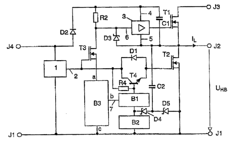
Figure 4 represents an exemplary embodiment for a
half-bridge inverter that, in accordance with the
invention, detects the minimum _Ln the half-bridge
output voltage rTHB. By comparison with figure 2, the
series circuit of two diodes D4 and D5 .is connected in
parallel with the block B2. The trapezoidal capacitor
CA 02434108 2003-06-30
- 27 -
C2 is connected not directly to the reference potential
Jl, but to the tie point of D4 and D5. Together with
the block B2, D4 and D5 canstitute an apparatus for
acquiring the current through the trapezoidal
capacitor. At the instant when the upper half-bridge
switch T1 is switched off, the trapezoidal capacitor is
charged and begins to be discharged by the: load current
IL via the diode D5. If the load curreni~ IL does not
succeed in completely discharging the trapezoidal
l0 capacitor, the load current IL changes polarity as
indicated by reactances included in the load circuit.
At this instant, a recharging operation of the
trapezoidal capacitor C2 begins via the diode D4 and
the block B2. The resulting voltage drop across the
block B2 raises the potential of the reference
electrode of the time delay switch in the block B1.
According to the invention, the result of this is to
switch off the time delay switch in the block B1. The
blocking of the control input of t:he interrupt
initiation switch T4 by the time delay switch in the
block B1 is thereby canceled, and the interrupt
initiation switch T4 is switched on by the control
module 1 via the resistor R4. Accoi:ding to the
invention, the operation described succeeds in
switching on the lower half-bridge transistor T2 at the
minimum in the half-bridge output voltage UHB. It is
preferred to use Schottky diodes for' the diodes D4 and
D5 in order to keep the forward voltages low, the
result being to enable early detection of the minimum
in the half-bridge output voltage UHB.
The above statements relate throughout t;o half-bridge
inverters. However, the inventive ideas can also be
transferred to full-bridge inverters.