Note: Descriptions are shown in the official language in which they were submitted.
CA 02434161 2003-07-18
WO 02/066256 PCT/US02/01409
Process for the Manufacture of Printed Circuit Boards
with Plated Resistors
FIELD OF INVENTION
The present invention relates to a process for the manufacture of double-sided
or
multilayer printed circuit boards with printed plated resistors. The method
proposed
produces printed circuits with integral resistors, which are printed and
plated in place on
the surfaces of the printed circuit board, or on the inner cores of multilayer
printed circuit
boards thereby opening the area on the surface of the board for placement of
active
devices. The process produces printed circuit boards with resistors in a
manner that is
more efficient and economical than previously possible.
BACKGROUND OF THE INVENTION
In the manufacture of printed circuits, it is now commonplace to provide
planar
boards having circuitry on each side thereof (e.g. double-sided circuit
boards). It is also
commonplace to produce boards comprised of integral planar laminates of
insulating
substrate and conductive metal, wherein one or more parallel innerlayers or
planes of the
conductive metal, separated by insulating substrate, are present within the
structure, with
the exposed outer surfaces, along with the inner planes, of the laminate
containing printed
circuit patterns (e.g. multilayer circuit boards).
In double sided and multilayer circuit boards, it is necessary to provide
interconnection between or among the various layers and/or sides of the board
containing
the conductive circuitry. This is achieved by providing metalized, conductive
thru-holes
in the board communicating with the sides and layers requiring electrical
interconnection.
The predominantly employed method for providing conductive thru-holes is by
electroless
deposition of metal on the non-conductive surfaces of the thru-holes, which
have been
drilled or punched through the board. Typically the electroless deposition is
followed by
electrolytic deposition of metal in the holes to build conductive metal to the
required
thickness. Recently some processes have allowed for direct electroplating in
the thru-
holes without need for prior electroless deposition.
The typical manufacturing sequence for producing printed circuit boards begins
with a copper-clad laminate. The copper clad laminate comprises a glass
reinforced epoxy
1
CA 02434161 2003-07-18
WO 02/066256 PCT/US02/01409
insulating substrate with copper foil adhered to both planar surfaces of said
substrate,
although other types of insulating substrates such as paper phenolic and
polyimide, have
been used. First the thru-holes are drilled or punched in the copper clad
laminate thereby
exposing the hole surfaces of insulating substrate material. The holes are
then subjected to
a chemical plating process which deposits conductive metal in the holes as
well as on the
copper surfaces. A plating mask is provided on the outer surfaces in the
negative image of
the circuitry desired. Subsequently copper is electroplated on all surfaces,
not covered by
the plating mask, to a predetermined thickness, followed.by a thin deposition
of tin to act
as an etch resist. The plating resist is then stripped and the exposed copper
surfaces (i.e.,
those not plated with the etch resist) are etched away. Finally the etch
resist is removed
and printed circuit board is finished with one of a number of known finishing
methods
such as solder mask, followed by hot air solder leveling. The foregoing
process is
typically called the pattern plate process and is suitable for producing
double-sided printed
circuit boards or multilayer boards. However, in the case of multilayer boards
the starting
material is a copper clad laminate which comprises inner planes of circuitry
called
innerlayers.
Simple printed circuit boards and the innerlayers of a multilayer circuit
board are
produced through a technique called print and etch. In this manner a
photopolymer is
laminated or dried on the copper surfaces of a copper clad laminate. The
photopolymer is
then selectively imaged using a negative and developed to produce a positive
image of the
desired circuit pattern on the surfaces of the copper clad laminate. The
exposed copper is
then etched away and the photopolymer stripped, revealing the desired circuit
pattern.
°The semi-additive process may be used in conjunction with the print
and etch
process to produce double sided or multilayer print and etch boards with
plated thru-holes.
In this process a copper clad laminate or a multilayer package with copper
foil on the
exterior surfaces is processed through the print and etch process as given
above. Holes are
then drilled in the board in a desired array. A plating resist applied to
cover substantially
the entire outer surfaces of the board except for the holes and the circuits.
Typically, a
separate desensitizing mask is applied, the. holes are activated and the
desensitizing mask
is then stripped away without disturbing the activation. The exposed areas are
then plated
electrolessly.
In addition to the foregoing, many other processes have been utilized to
produce
printed circuit boards. Some of these processes are detailed in U.S. Patent
Nos. 3,982,045,
2
CA 02434161 2003-07-18
WO 02/066256 PCT/US02/01409
4,847,114 and 5,246,817, the teachings each of which are incorporated herein
by reference
in their entirety. However, in the prior art processes, the circuits are made
such that
resistors, if required, need to be provided externally from the circuit board
itself. (e.g.
mounted on the surface of the circuit board as an appendage).
A process whereby reliable resistors can be printed and plated as an integral
part of
the circuitry of the printed circuit board is disclosed herein. This provides
for an efficient
and economical way of providing the necessary resistors. In addition the
process provides
for further miniaturization of the printed circuit boards produced in
comparison to those
produced by prior art methods. Typical prior art in this regard are U.S.
Patent Nos.
3,808,576 and 2,662,957, the teachings both of which are incorporated by
reference herein
in their entirety. This invention produces printed circuits with integral
resistors, which
resistors have a particularly constant resistance as is required by the most
demanding
applications.
BRIEF DESCRIPTION OF THE FIGURES
Collectively the figures visually show the steps of the basic process of this
invention.
Figure 1A represents one side of the copper clad laminate (although both sides
would most likely be processed in the same way) with insulating dielectric
substrate, 10,
and the attached copper foil, 11.
Figure 1B indicates the presence of an imaged resist, 12, on the copper foil,
11.
The resist, 12, has already been imaged and developed and therefore covers
only the
desired portions of the copper foil, 11.
Figure 1 C indicates that the exposed copper has now been etched away leaving
unconnected resist covered copper~traces, 13 and 14 on the substrate, 10.
Figure 1D indicates that the resist has now been completely stripped away
leaving
only the desired copper traces, 13 and 14 on the substrate, 10.
3
CA 02434161 2003-07-18
WO 02/066256 PCT/US02/01409
Figure 1E shows the application of a plating resist, 15, which covers the
entire area
of the board except the portions where the resistor will be plated.
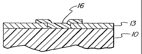
Figure 1F shows the plated resistor, 16, connecting the previously unconnected
copper traces, 13 and 14.
Figure 1 G shows the circuit after the plating resist has been stripped away.
SUMMARY OF THE INVENTION
The current invention proposes a process for printing and plating resistors as
an
integral part of a printed circuit board. The foregoing process is described
in its basic form
by the following sequence of processing steps:
a). Apply an etch resist (12) onto the copper foil (11) surface of a metal
clad .
laminate (or multilayer package) in a desired pattern. The desired pattern
should preferably define the conductive circuits desired in a positive
° manner and should define the areas between the circuits and locations
for
the resistors in a negative manner;
b). Etch away the exposed copper and preferably remove the etch resist to form
unconnected copper traces (13 and 14);
c). Activate the surfaces to accept plating thereon;
d). Apply a plating mask (15) which covers substantially all of the surfaces
except for the areas where the resistors are to be plated;
e). Plate the exposed areas with a resistive material (16); and
Strip away the plating mask.
As an equivalent to the foregoing process, foregoing steps a and b can be
replaced
by an additive process with the following steps:
a.1.). Activate the surfaces of a bare dielectric substrate to accept plating
thereon;
a.2.). Apply a plating mask to the dielectric substrate such that the desired
circuits are defined in a negative manner and the areas between the
4
CA 02434161 2003-07-18
WO 02/066256 PCT/US02/01409
circuits and the locations for the resistors are defined in a positive
manner;
a.3.) Plate the desired circuitry;
a.4.) Strip away the plating resist; and
Subsequently follow steps (c) through (f) noted previously.
In a preferred embodiment the substrate is subjected to a dielectric etchant
after
step b but before step c in order to uniformize the dielectric surface.
Etching at this point
to uniformize the dielectric surface will provide plated resistors with more
constant and
predictable resistance.
In another preferred embodiment, the plated resist material is contacted with
an
oxidant between steps (e) and (f) or after step (f). Contacting the plated
resist material
with an oxidant, and thereby oxidizing the plated resist material in a
controlled manner
provides plated resistors with more constant and predictable resistance and
optionally with
higher resistance if desired. Intrinsic resistance increases via controlled
oxidation.
Alternatively, or in addition, the resistors can be baked a this point, after
step f, to stabilize
the resistance of the resistors
In a third preferred embodiment, the printed circuit board is subjected to a
cleaning
step after step (f) in order to remove any residual activator species from
step (c) and to
otherwise improve the surface insulation resistance of the board in general.
The inclusion
of this step produces printed circuit boards with higher reliability.
Finally trimming is suggested as a method for adjusting the insulation
resistance of
the plated resistors to within a prescribed range of insulation resistance
(ohms). Ablating
portions of the plated resistor using laser light is a particularly preferred
method of
trimming.
DETAILED DESCRIPTION OF THE INVENTION
The processes described herein provide a method of forming a resistor between
two
conductive areas, which areas are upon and separated by an insulating
substrate. ~ The
method described provides for plating a resistive material onto the insulating
substrate,
which is between the conductive areas, such that the resistive material
connects the
conductive areas. The processes described are particularly useful in producing
printed
5
CA 02434161 2003-07-18
WO 02/066256 PCT/US02/01409
circuit boards with plated resistors which are integral with the circuits. The
most basic
processing sequence is described as follows:
a). apply an etch resist onto the surfaces of a metal clad laminate such that
the
resist defines the desired circuits in a positive manner and the areas
between the circuits, including the locations for the resistors, are defined
in
a negative manner;
b). etch away exposed copper surfaces and preferably strip the etch resist;
c). optionally, treat the exposed dielectric surfaces with a process selected
from
the group consisting of chemical etching, plasma etching, laser
normalization, vapor blasting, sanding, shot blasting and sand blasting;
d). activate the exposed dielectric surfaces to accept plating thereon;
e). apply a plating resist such that the plating resist covers all or
substantially
all of the surfaces except for the areas where the resistors are to be plated
(i.e. such that the resistor areas are defined in a negative manner;
f). plate the exposed areas;
g). optionally, contact the plated areas with an oxidant;
h). strip away the plating mask;
i). optionally clean the surfaces of the printed circuit board;
j). optionally, bake the resistors;
k). optionally, trim portions of the plated resistor material such that the
final
insulation resistance of the resistors falls within a predetermined range of
insulation resistance; and
1). optionally, coat the resistors with a protective coating.
Steps (a) and (b) together call for the creation of defined circuitry on the
surfaces
of a metal clad dielectric laminate (or multilayer package - several layers of
circuitry
containing one or more innerlayers of circuitry which have been laminated into
a single
planar package). The irinerlayers may or may not contain the plated resistors
of this
invention. If so, then the innerlayers may be fabricated by the process
described herein.
Collectively metal clad dielectric laminate and multilayer packages are
referred to as metal
clad laminate. 'The metal clad laminate may optionally have thru holes in it
in a desired
array. The thru holes may or may not be plated at this point. The key here is
the
6
CA 02434161 2003-07-18
WO 02/066256 PCT/US02/01409
definition and creation of circuit patterns on the surfaces of the metal clad
laminate along
with the definition and creation of specific breaks in the circuitry where the
resistors will
be plated (the "resistor areas"). The length and width of the specific
resistor areas will
obviously directly impact the resistance achieved after plating.
The definition and creation of circuitry and the resistor areas can be
accomplished
in many ways. The most prevalent way is through the subtractive process as
described in
current steps (a) and (b). In the subtractive process, a metal (usually
copper) clad laminate
is used. The metal clad laminate comprises a planar dielectric substrate with
metal foil
adhered to both exterior surfaces. As discussed, the dielectric substrate is
typically glass
reinforced epoxy, but can also be a variety of other insulative materials
known in the art.
In any case, a resist pattern is applied to the metal surfaces of the metal
clad laminate such
that the resist defines the circuits in a positive manner, and the areas
between the circuits
and the resistor areas in a negative manner. The most typical way of
accomplishing this is
to use a photoresist. In this case the photoresist is applied to the metal
surfaces in either
liquid or dry form. The photoresist is then selectively exposed to actinic
radiation through
a negative. The unexposed areas of the resist are developed away revealing the
desired
pattern. As an alternative, the resist may be screened onto the metal surfaces
directly in
the desired pattern. After the circuits are defined with the resist, the
exposed copper areas
are etched away and the resist is stripped revealing the circuits. Thus the
areas between
the circuits and the resistor areas are now bare dielectric.
Step (c) is optional, but recommended. In order for the resistors to be usable
and
reliable, the resistance must be predictable, relatively constant and
reliable. In order to
achieve plated resistors with particularly predictable, relatively constant
and reliable
resistance, the dielectric surface to be plated with the resistive material to
form the resistor
must be uniform. Dielectric surface uniformity and predictable, relatively
constant and
reliable resistance of the plated resistors can be accomplished by
uniformizing the
dielectric surface upon which the resistor is to be plated. Uniformizing can
be achieved in
several ways such as vapor blasting, chemical etching, plasma etching, laser
normalization
or mechanical uniformization. Mechanical uniformization can be achieved by
sanding,
sand blasting or shot blasting. Surface uniformization through chemical
etching is
generally the most reliable and efficient means. The particular etchant used
in this regard
must be matched with the dielectric being used. However, if glass reinforced
epoxy is
used, the inventors have found that alkaline permanganate, concentrated
sulfuric acid,
7
CA 02434161 2003-07-18
WO 02/066256 PCT/US02/01409
chromic acid or plasma to be particularly useful in etching and uniformizing
the surface of
the dielectric. Solutions of sodium or potassium permanganate at
concentrations in excess
of 50 grams/liter, in 10% by weight caustic solution, at temperatures in
excess of 140°F
and for times of 2 to 20 minutes are preferred in this regard. If
permanganates are used in
this regard they may be preceded with a swellant or sensitizer which makes the
dielectric
more susceptible to the permanganate etch. A typical swellant for epoxy is m-
pyrol
applied full strength- at from 90-120 °F for from 1 to 5 minutes. In
addition the
permanganate etch is typically followed by an acid reducing solution which
will remove
the permanganate residues.
Step (d) involves activating the surfaces to be plated. Activation of the
surfaces
can range in complexity from a single dip in a precious metal activator (or
non-precious
metal or other activators know in the art) to a full plating cycle involving
numerous steps.
Typically the activation process will begin with a conditioner (surfactant or
other type),
followed by an activator (PdC 12/SnC 12 Colloid, or ionic solution of
palladium or another
precious metal) and an accelerator. If an accelerator is used, the inventors
have found that
it is preferable to apply the accelerator solution, immediately prior to step
(f) (i.e. the
plating of the resistors). Electroless plating accelerators are generally
known in the art and
include simple solutions of hydrochloric or fluoboric acid or alkaline
solutions of sodium
chlorite. Clean water rinses are interposed between each chemical treatment.
Regardless
of the activation cycle chosen, its primary purpose is to treat the surfaces
such that they
initiate and accept plating. A wide variety of methods for achieving this are
known in the
art, any of which may be advantageously utilized here. Please refer to U.S.
Patent Nos.
5,032,427 (I~ukanskis, et al.), 4,976,990 (Bath et al.) and 4,863,758
(Rhodenizer), the
teachings of which are incorporated herein by reference in their entirety. The
inventors
have found it beneficial to dry the metal clad laminate after the activation
cycle of step (d).
In step (e) a solid or liquid plating mask is applied such that the resistor
areas are
defined in a negative manner. Generally, to accomplish this, the plating mask
covers all or
substantially all of the surfaces except for the resistor areas. The plated
resistors are more
reliable if the plating mask allows for some plating overlap where the
resistive plating
meets the conductive circuit as opposed to covering all of the circuit with
plating mask and
causing the resistive plating to merely abut the conductive circuit. In any
case, the plating
mask can be any typical plating mask known in the art as long as it maintains
its integrity
in the subsequent plating bath. The plating mask may be screened onto the
surface in the
8
CA 02434161 2003-07-18
WO 02/066256 PCT/US02/01409
desired pattern or blanket coated, photoimaged and developed. In applying a
solid plating
mask to the surface, the inventors have found vacuum lamination to be
particularly useful
in insuring that the mask conforms closely to the three dimensional features
of the surface.
Step (f) involves plating the resistors. At this stage the plating will occur
only on
the areas not covered by the plating mask which was applied in step (e) (i.e.
the resistor
areas, preferably with some overlap onto the circuits where the resistor
connects to the
circuits). A variety of plating baths can be advantageously utilized.
Electroless nickel-
phosphorous, (or alloys thereof) electroless precious metal plating baths,
including
palladium-phosphorous, or ruthenium-phosphorous (or alloys of any of the
foregoing)
electroless plating baths, are particularly useful in this regard. It may be
optionally
desirable to clean and/or accelerate the surfaces immediately prior to
plating.
Obviously, the thickness of the metal plated has a direct impact on the
resistivity of
the resultant resistor. The inventors have found that typically it is
advantageous to plate
metal thickness in the range of from 0.05 to 2.5 microns, preferably from 0.10
to 1.0
microns and most preferable from 0.10 to 0.50 microns. Plating advantageously
takes 2 to
3 minutes, more preferably 5 to 10 minutes depending upon the plating bath
used and the
ultimate resistance desired.
Depending upon the ultimate resistance desired, the following factors may be
adjusted to vary the resistivity of the resultant resistor: type of metal
plated, thickness of
the metal plated, length of the resistor, width of the resistor and subsequent
treatment of
the resistor. With regard to type of metal plated, the phosphorous content of
the nickel-
phosphorous, palladium phosphorous, or the ruthenium - phosphorous, will
affect the
resistivity of the final deposit. All of the foregoing factors may be varied
to achieve the
ultimate resistance desired. The inventors have found that the intrinsic
resistance of the
nickel, palladium or ruthenium plated increases with the phosphorous content
of the metal.
They have also found it most advantageous to plate the resistors with nickel
having a
phosphorous content of 10-13% by weight and palladium with a phosphorous
content of 2-
8% by weight. The inventors have found that high phosphorous containing
metals,
particularly nickel or palladium, produce a plated coating with relatively
high intrinsic
resistance. Therefore, for any given desired ultimate resistance for the
resistor, a greater
thickness of material (holding length and width constant) can be plated,
thereby yielding
more reliable plated resistors. This also allows for commercially acceptable
plating times
in the range of 2-3 minutes. Plating times of less than 2-3 minutes are too
short to easily
9
CA 02434161 2003-07-18
WO 02/066256 PCT/US02/01409
control in a commercial process with reliability, thereby producing relatively
unreliable
plated resistors. If resistors of different resistance's are required on the
same circuit board,
then steps (e) and (f) or (d), (e) and (f) can be repeated to plate different
resistors with
different thickness of resistive material or with different resistive
material. Alternatively,
of course, other variables such as length and width of the resistors can be
varied without
repeating any steps.
Step (g) optionally provides for controlled oxidation of the plated resistor
metal
preferably by controlled chemical oxidation. Controlled oxidation is a method
for
increasing the resistivity of the plated resistor and more importantly of
providing for more
predictable resistance on a consistent basis. In this regard a variety of
oxidants may be
used including potassium iodate, which is preferred. If potassium iodate is
used, an
aqueous solution with from 10-75 gr/1 potassium iodate at a temperature of
90°C and for a
time of 5 minutes has proven effective. The higher intrinsic resistance
materials allow for
greater thickness of plated material (other variables' constant), more
reliable plated
resistors and commercially acceptable plating times. Increases in intrinsic
resistance of the
plated metal of from 20 to 400 percent based upon the intrinsic resistance of
the same
unoxidized metal can be achieved.
Step (h) involves stripping away the plating mask. A stripping solution must
be
chosen to match the plating mask used. Typical plating masks can be stripped
away in
alkaline solution, however some require organic solvents. .
In step (i), it is optionally advantageous to clean the surfaces of the
printed cixcuit
board in order to remove any residual activator and to increase the surface
resistance of the
board. U.S. Patent Numbers 5,221,418; 5,207,867; and 4,978,422, the teachings
each of
which are incorporated herein by reference in their entirety, all teach
various means of
cleaning and increasing the surface resistance of boards as is suggested by
step (i) herein.
Care must be taken such that the resistance of the plated resistor is not
affected by the
foregoing cleaning. It may be advantageous to protect the plated resistors,
prior to
cleaning the board, through use of a coating of some type, permanent or non-
permanent.
Thus, step (i) may be conducted after step (h) as shown or may be conducted
after step (1)
when the resistors have been coated with an appropriate protective coating.
However,
unless the resistors are protected, no further chemical processing should
preferably occur
after trimming, since further processing may affect the insulation resistance
of the
resistors.
CA 02434161 2003-07-18
WO 02/066256 PCT/US02/01409
As stated, it is typically of great importance that the resistivity of the
plated
resistors be predictable and constant over time. The inventors have discovered
that
subsequent processing of the printed circuit boards can cause the resistance
of plated
resistors to change. In particular, the lamination and soldering processes can
permanently
change the resistance of the resistors. In addition, the inventors have found
that baking the
resistors after they have been plated can stabilize the resistance of the
resistors such that
changes in resistance due to subsequent processing are minimized. Thus, the
inventors
prefer to bake the plated resistors from 30 minutes to 3 hours at from
100°F to 400°F,
preferably for 30 minutes to 1.5 hours at from 300°F to 400°F,
in order to stabilize the
resistance of the resistors and minimize any subsequent changes therein. Any
change in
resistance as a result of baking the resistors, or other subsequent
processing, must be
anticipated in designing the resistors. Final changes in the insulation
resistance of the
plated resistor can be achieved through trimming.
After baking, or after plating if baking is not desired, the resistance of the
plated
resistors can be measured and adjusted, if necessary, by trimming. Trimming is
a method
of increasing the insulation resistance of the plated resistors to a
predetermined or
specified resistance value by trimming, or removing, in a controlled fashion,
a portion of
the plated resistor such that the specified insulation resistance value is
achieved for the
device. The trimming or controlled removal is typically accomplished by use of
lasers. In
this regard, lasers are used to ablate portions of the plated resistor in a
precise and
controlled manner such that the desired resistance is achieved. Plated
resistors are
particularly amenable to this form of laser ablation since the plated films
are generally
relatively thin (i.e., about 5 to 25 microinches). In the alternative, the
plated resistors can
be trimmed using any method which can reliably remove portions of the plated
resistor in
a controlled manner. Most preferably, the trimming step will occur as close to
the end of
the printed circuit processing as possible in order to minimize the
possibility of the
resistance value changing.
Finally, it is usually desirable to coat the surfaces of the board, including
the plated
resistors, with a protective coating such as a soldermask. Soldermasks are
desirable for
the protection of the board in subsequent processing and to enhance the
durability of the
resulting product. Typical solder mask processing is described in U.S. patent
No.
5,296,334, the teachings of which are incorporated herein by reference in
their entirety.
11
CA 02434161 2003-07-18
WO 02/066256 PCT/US02/01409
Resistivity is the inverse value of conductivity. It is commonly expressed by
volume resistivity, surface resistivity and/or insulation resistance as
provided for under
ASTM D 257. Volume resistivity is the resistance between the faces of a unit
cube and is
equal to V=AR/X were V is the volume resistivity expressed in ohms-cm, A is
the cross
sectional area of the electrical path (cmz), R is the measured resistance
(ohms), and X is
the length of the electrical path. Values for volume resistivity for the
resistors plated as
described in this invention can range from about 500 to about 1x10 ohm-cm, and
preferably range from about 5 to about SxlO-4 ohm-cm, most preferably range
from about
1x10⁻² to about 1x10⁻³ ohm-cm. Surface resistivity is the ability of an
insulator to resist the
flow of a current in its surface and is equal to S = PR/d where S is the
surface resistivity
expressed in ohms/square, P is a parameter of the guarded electrode (cm) given
in ASTM
D 257, R is the measured resistance (ohms) and D is the distance between the
electrodes
(cm). Insulation resistance is measured on a specific device or configuration
and is the
integrated effect of volume and surface resistivity. Insulation resistance is
usually
expressed in ohms and relates to a specific device or configuration. The
resistors plated as
described in this invention have an insulation resistance which ranges from
about 1 to
about 10,000 ohms, preferably from about 10 to about 1,000 ohms.
In applying the foregoing principles to a particular plated resistor with a
particular
desired design resistance (i.e. insulation resistance) the following equation
is useful:
R = _VX
A
where R = the overall desired resistance of the specific plated resistor (i.e.
its insulation resistance).
V = volume resistivity of the plated deposit and is generally approximately
constant for a particular plating solution.
X = plated resistor length
A = plated resistor cross sectional area (width x thickness)
A typical example may require a plated resistor of 0.005 inches in width,
0.005
inches in length and an overall desired resistance of 275 ohms + 15 ohms.
Using a plating
solution that deposits a modified electroless nickel-phosphorous deposit with
a volume
resistance of about 7x10⁻³ ohm-cm and depositing a thickness of 10 microinches
of the
12
CA 02434161 2003-07-18
WO 02/066256 PCT/US02/01409
foregoing electroless nickel, a resistor of the desired overall resistance may
be obtained as
follows:
R = (0.007 ohm-cm~(0.005 ina x 1 in
SxlO-8 inz 2.54 cm
R = 276 ohms
If further increases in resistance are required, then the so plated deposit
may be
oxidized as discussed herein. It should be noted that the key to reproducible
results in this
regard is surface normalization prior to plating said surface and baking the
plated resistors
until resistance stabilization is achieved, all as discussed herein. Post
oxidation of the
deposit can also increase resistance and improve reproducibility. Necessary
adjustments
to the resistance of the plated resistors can be made by trimming as noted
herein.
For comparison purposes, the volume resistivity of plated copper circuitry or
copper plated through holes on a printed circuit board is typically less than
about SxlO-5
ohm-cm and can preferably range from about 1x10⁻⁶ to about 1x10⁻⁸ ohm-cm. The
volume resistivity of the insulative substrate of an FR-4 epoxy-glass printed
circuit board
is typically greater than about 109 ohm-cm and can preferably range from about
I09 to
about 102° ohm-cm.
With the pace of minaturization of electronic devices, the surface area of
printed
circuit boards has become more compacted and more valuable. As a result, the
overall
size of resistors plated in accordance with this invention must fit the size
requirement of
ever-shrinking printed circuit boards. Plated resistors, prepaxed in
accordance with this
invention, with volume resistivity in the range of 500 to 1x10⁻⁴ ohm-cm can be
formed
with lengths ranging from about 0.002 in. to about 1.0 in., preferably from
about 0.005 to
about 0.20 in., most preferably from about 0.005 to about 0.080 in. with
widths ranging
from about 0.002 to about 1.0 in., preferably from about 0.005 to about 0.20
in., most
preferably from about O.OOS.to about 0.080 in. and with thickness ranging from
about 2 to
about 300 microinches, preferably from about 5 to about 100 microinches and
most
preferably from about 5 to about 25 microinches. Typically, the foregoing
length and
width dimensions are imaged dimensions (i.e. dimensions of the imaged plating
mask in
13
CA 02434161 2003-07-18
WO 02/066256 PCT/US02/01409
the area to be plated with resistive material). Actual dimensions of the
plated resistor may
vary somewhat.
The following examples are presented for illustrative purposes only and should
not
be taken as limiting in any way:
EXAMPLE I
Copper clad glass reinforced epoxy laminates were processed through the
following sequence:
1. A dry film resist (Aquamer CF-1.5 available from MacDermid, Inc.) was
laminated to both copper surfaces of copper clad laminate. The resist was
then selectively exposed to ultraviolet light by exposure through a negative.
The negative was designed such that the ultraviolet light impinged upon the
circuit areas only. (i.e. circuits defined in a positive manner and the areas
between circuits and resistor areas are defined in a negative manner) The
unexposed portions of the resist were developed away using a 1 % by
weight potassium carbonate solution at 90°F for 30 seconds.
2. The exposed copper surfaces were etched away by spraying ammoniacal
copper chloride etchant at 110°F onto the surfaces until the exposed
copper
was cleanly etched away. The resist was then stripped away in a 10% by
weight caustic solution.
3. The surfaces were activated to accept plating thereon by the following
processsequence:
a). MacDermid M-Conditioner, 110°F, 2 minutes
b). MacDermid M-Preactivator, 75°F, 2 minutes
c). MacDermid M-Activator, 100 °F, 5 minutes
Clean water rinses were interspersed between each of the foregoing steps.
4. MacDermid Viatek PM#4 plating mask was then screened onto the surfaces
such that it covered all of the surfaces except for the areas where the
resistors
14
CA 02434161 2003-07-18
WO 02/066256 PCT/US02/01409
were to be plated (the "resistor areas") (i.e. such that the resistor areas
were
defined in a negative manner). The plating mask was then baked to cure for 5
minutes at 250 °F. The width and length of the resistor areas,
resistivity of
electroless palladium-phosphorous, and the thickness of the palladium-
phosphorous plate were used to design and predict the ultimate resistance of
the plated resistors.
5. The resistor areas were then plated by immersion in MacDennid Pallas 52
electroless palladium-phosphorous plating bath, which was prepared per the
supplied data sheet, at 150 °F for 5 minutes. Approximately 0.1 to 0.2
microns of electroless palladium-phosphorous were plated.
6. The plating mask was then stripped away using a 10% by weight caustic
solution at 150 °F for 2 minutes and then thoroughly rinsed.
The laminates were then electrically tested to determine the actual resistance
of the
plated resistors and the actual resistance was compared to the design
resistance. Variances
of 25-30% were recorded.
EXAMPLE II
Copper clad glass reinforced epoxy laminates were processed through the same
sequence as in Example I except that after step 2 and before step 3 the
following additional
processing was inserted:
a). M-Pyrol, 100% be weight, 90°F, 2 minutes
b). Potassium pernianganate, 60 gr/1, 10% by weight caustic soda,
160°F, 10 minutes
c). 10% by weight hydrochloric acid, 5 gr/1 hydroxylamine sulfate,
110°F, 5 minutes.
CA 02434161 2003-07-18
WO 02/066256 PCT/US02/01409
The laminates were then electrically tested to determine the actual resistance
of the
plated resistors and the actual resistance was compared to the design
resistance. Variances
of 8-10% were recorded.
The laminates were further processed by interleaving glass-reinforced epoxy
pre-
preg sheets between several laminates and between the laminates and copper
foil capping
sheets, resulting in a multilayer package. 'The multilayer package was then
subjected to
heat and pressure in order to melt and cure the interleaved pre-preg layers.
The actual
laminates were then again electrically tested, after isolating the resistors,
to determine the
actual resistance of the plated resistors and the actual resistance was
compared to the
design resistance. Variances of 20-30% were recorded.
EXAMPLE III
Copper clad glass reinforced epoxy laminates were processed through the same
sequence as in Example II except that at the end of the processing as
indicated in Example
II, the following sequence was performed:
The resistors were oxidized by immersing the boards
in an aqueous solution of 40 gr/1 of potassium iodate at
90°C for 5 minutes.
The laminates were then electrically tested to determine the actual resistance
of the
plated resistors (without subsequent lamination). Actual resistance has
increased by 300%
as compared to the unoxidized resistors of Example II. Variances of 5 to 10 %
were
recorded.
EXAMPLE IV
Copper clad glass reinforced epoxy laminates were processed through the same
sequence as in Example II, except that after Step 6, the laminates were baked
at 350°F for
one hour.
16
CA 02434161 2003-07-18
WO 02/066256 PCT/US02/01409
The laminates were then electrically tested to determine the actual resistance
of the
plated resistors and the actual resistance was compared to the design
resistance. Variances
of 5-10% were recorded.
The laminates were further processed by interleaving glass reinforced epoxy
pre-
preg sheets between the several laminates and between the laminates and copper
foil
capping sheets, resulting in a multilayer package. The multilayer package was
then
subjected to heat and pressure in order to melt and cure the interleaved pre-
preg layers.
The actual laminates were then again electrically tested, after isolating the
resisters, to
determine the actual resistance of the plated resisters and the actual
resistance was
compared to the design resistance. Variances of 5-10% were recorded.
17