Note: Descriptions are shown in the official language in which they were submitted.
CA 02434214 2003-07-07
Device and method for analyzing ion channels in membranes
Field of the invention
The present invention relates to devices and methods for analyzing ion
channels in mem-
braves, in particular devices and methods for executing the so-called patch
clamp tech-
nique with the aid of a biochip, especially for use in high throughput
processes.
Prior art
Ion channels are membrane proteins which serve as switchable pores for a flow
of current.
Ion channels, which are the smallest excitable biological structures,
especially constitute the
fundamental switching elements of the nervous system. It follows that the
equipment of a
neurocyte with ion channels of different types essentially determines the
neurocyte's role in
the processing of information in the brain. This applies, by the way, also to
non-neuron ex-
citable cells in a similar manner, e.g. to those of the cardiac muscle and its
stimulus con-
duction systems. Switching processes in ian channels are analyzed for
obtaining e.g. infor-
mation on possible malfunctions and their elimination by means of drugs and
the like.
For analyzing ion channels in cell membranes with respect to their switching
processes, i.e.
their opening and closing mechanisms, the patch clamp method is used in the
prior art. For
this purpose, so-called patch clamp pipettes consisting of glass are used.
Such a pipette is
shown in Fig. 5. This pipette comprises an opening 59 having a diameter of
approx. 1 Nm.
In addition, the pipette comprises a pipette shaft 58 in which an electrode 53
is provided.
For analyzing an ion channel, a membrane patch is sucked up by means of such a
pipette
filled with an electrolyte so that a close contact will be established between
the membrane
and the glass. In this way, a very high sealing resistance of an order of
magnitude of > 1
GS2 is obtained. This permits measurement of very small ion currents, down to
a few 100 fA,
through the membrane.
The known device is, however, disadvantageous insofar as it is not suitable
for simultane-
ously analyzing a large number of substances or the effect of a substance on a
large num-
ber of different (e.g. genetically modified) ion channels. The known device is
therefore not
CA 02434214 2003-07-07
2
suitable for high throughput analyzing. Hence, this device is can be used for
substance
screening in the pharmaceutical industry only to a very limited extent.
Another disadvantage of the known device is that the time scale on which the
opening and
closing mechanisms in the ion channels take place is accessible only to a very
limited ex-
tent with this device consisting of a glass pipette, an electrode and an
amplifier. This has
the effect that, When this device is used for the patch clamp method, the
bandwidth will be
limited to less than 100 kHz. For analyzing the opening and closing mechanisms
in ion
channels, time scales corresponding to a bandwidth of > 1 MHz would, however,
be desir-
able.
It is therefore the object of the present invention to provide a device for
analyzing ion chan-
nels in cell membranes, which is suitable for high throughput processes, e.g.
for use in the
pharmaceutical industry, andlor which exhibits an improved signal-to-noise
ratio and an
improved timing resolution.
Description of the invention
This object is achieved by a biochip for analyzing ion channels, comprising a
substrate in
which openings are provided in the form of an MxN array for receiving therein
a cell mem-
brane including at least one ion channel or for receiving therein an
artificial lipid membrane
including at least one ion channel, wherein M >_ 1 and N > 1.
When such a biochip is used, the use of a pipette whose comparatively long
shaft leads to a
high stray capacitance can be dispensed with. The critical geometrical
parameters can,
however, be optimized from the very beginning, and this has the effect that
the signal-to-
noise ratio will be improved markedly in comparison with the prior art whereby
the timing
resolution will be improved. This applies to biochips with a single opening,
i.e. for M = N = 1
as well as to biochips with a plurality of openings, i.e. M > 1 and/or N > 1.
Due to the plurality of openings for receiving therein membranes including ion
channels, it
will additionally be possible to parallelize the patch clamp technique in the
case of M > 1
and/or N > 1, whereby MxN measurements can be carried out simultaneously with
one chip.
CA 02434214 2003-07-07
In this case it will be particularly advantageous to adapt the shape of this
MxN array to the
geometry of the 96, 384 or 1536 cuvette plates used as a standard in the
pharmaceutical
industry. These cuvette plates can be inserted into automatic pipetting
devices by means of
which substances can advantageously be applied to the biochip described here.
A special
advantage is that, by means of automatic pipetting devices or by other arrays
of pipettes or
cannulae which are arranged in a fixed mode relative to one another, solutions
or cells can
be taken simultaneously from a plurality of cuvettes of the standard cuvette
plates and ap-
plied to the biochip, since the arrangement of the pipettes or cannulae
relative to one an-
other can be maintained for applying the solutions or cells to the biochip.
In addition, membranes which have been applied to the biochip according to the
present
invention will, in comparison with the known device, be much more easily
accessible due to
the geometry of the biochip. This offers a much better possibility of
observing the mem-
branes and of manipulating them chemically and/or mechanically andlor
electrically.
According to an advantageous embodiment of the above-described biochip, the
surface has
in the area of each opening a means for improving the contact with the cell
membrane, said
means being provided on the receiving side of the respective opening and being
used for
guaranteeing improved adhesion of the membrane to the biochip in the area of
the aperture
(opening). Also the electrical sealing resistance can be increased in this
way.
In accordance with an advantageous further development, the means for
improving the
contact can be implemented in the form of a patterning of the surface.
For this purpose, the patterning can be provided in the form of one or a
plurality of rings
which is or which are arranged around each opening, or in the form of one or a
plurality of
squares or rectangles which is or which are arranged around each opening.
The patterning can especially be provided in the form of a depression in the
surface of the
biochip, said depression being arranged concentrically around and in closely
spaced rela-
tionship with the opening and having a diameter which is many times larger
than the di-
ameter of the opening so that the edge of the opening projects upwards beyond
the sur-
rounding biochip level. This has the effect that a cell membrane will be
dented by the edge
CA 02434214 2003-07-07
4
of the opening whereby the contact between the biochip and the membrane will
be im-
proved.
Each opening can have length and Width dimensions in the range of 10 Nm to 10
nm. The
number of ion channels observed can be adjusted in this way. In addition, a
smaller open-
ing will also reduce the membrane area and thus the capacitance and this will
improve the
measurement resolution still further.
The biochip according to the present invention is also excellently suitable
for forming artifi-
ciaf lipid membranes (artificial lipid bilayer) on the opening, this formation
taking place in
analogy with the known black lipid or lipid bilayer method. This permits ion
channels to be
analyzed by fusing vesicles, which include ion channels, with the artificial
lipid bilayer.
Due to the fact that the size of the aperture is small in comparison with the
known bilayer
method (in known devices the size of the aperture is normally > 100 Nm) and
due to the
resultant small capacitance, the signal-to-noise ratio can be improved.
In accordance with a preferred embodiment of the above-described biochip, each
opening
can be substantially circular. Such circular shapes can easily be implemented
in the bio-
chip. If a simple implementation is not necessary, also other shapes can be
chosen for the
cross-sections of the openings.
According to a preferred further development of all the above-described
biochips, the sub-
strate can comprises a base portion which has a first thickness and a window
portion or a
plurality of window portions which is/are formed in said base portion and
which has/have a
second thickness, an opening being provided in each of the respective window
portions.
The thickness of the base portion can here especially range from 1 mm to 100
Nm and the
thickness of the window portion can range from 1 pm to 50 Nm. This further
development
guarantees that the mechanical stability of the substrate will be preserved,
whereas the
length of the aperture (at right angles to the cross-section of the opening)
and thus also the
electric access resistance will remain as small as possible. In addition, this
further devel-
opment can be used for producing apertures with diameters of 10 pm down to
less than
1 Nm with the aid of a dry-etching step, laser ablation or Patent ion track
etching. On the ba-
sis of this further development it will also be possible to fill the aperture
more easily with the
CA 02434214 2003-07-07
electrolytic so4ution and to establish an electric contact therewith. The
depression formed on
the lower surface of the biochip by local thinning permits a simple
application of solutions by
means of a pipette; due to capillary forces, said solutions penetrate into the
aperture and fill
said aperture.
In accordance with an advantageous further development of all the above-
described bio-
chips, the substrate can comprise a semiconductor material, such as GaAs, Si
or AIGaAs,
or an insulator, such as glass or quartz, or polymers, such as polycarbonate,
acrylic glass
or polydimethylsiloxane (PDMS). A large number of advantages, in particular a
simple pro-
duction by means of a process technology perfected for the respective
material, can be
achieved by these materials.
According to an advantageous further development, the substrate comprising the
base por-
tion and the window portions formed in said base portion consists of one
material. The pro-
duction process of the biochip can be simplified in this way.
When a substrate consisting of a semiconductor material, in particular of Si,
GaAs or AI-
GaAs, is used, a passivating and insulating layer can be provided, said layer
being applied
to one surface or to both surfaces of the substrate. This insulating layer can
especially con-
sist of Si02, Ss3N4, glass or polymers, and of mufti-layer systems in which
these materials
are combined with one another and/or with the above-mentioned semiconductors
and/or
with metals, and have thicknesses of 50 nm up to several um. By means of these
materials,
a sealing resistance of a few G~2 can be realized, this kind of sealing
resistance being nec-
essary for measuring currents in the pA range.
In the production of this embodiment, the insulating layer can also fulfil the
function of an
etch stop layer and, in the case of anisotropic etching of the semiconductor
it can lead to
the formation of a window portion in which only the insulating layer is stilt
present. The ap-
erture can then be defined lithographically and the self-supporting insulating
layer can be
applied by dry-etching processes.
As a further advantageous alternative, polymers, such as polydimethyisiloxane
(PDMS),
can be used as a substrate material. When the above-described biochip is
produced from
PDMS, a 3D negative template (mould) is used, which has the inverted structure
of the de-
CA 02434214 2003-07-07
6
sired biochip. The PDMS is first viscous and, after having been mixed with a
curing agent, it
is cast into the mould and cured with or without heating (approx. 60 to
100° C). The flexible
biochip can then be released from the mould; said release can be carried out
more easily
when the mould has been coated with silanes previously. For the production of
this em-
bodiment a chemical modification of the surfaces (especially oxidation in the
plasma incin-
erator or also other suitable methods) will be advantageous.
Moreover, all the surfaces of the biochip may be provided with additional
insulating and
passivating layers of the above-mentioned materials and they may have chemical
modifica-
tions (silanization, oxidation).
According to a preferred further development of all the above-described
biochips, elec-
trodes can be provided on one or on both sides of the substrate. In
particular, electrodes
consisting e.g. of gold, silver or of other suitable metals can be applied
directly to the chip
by means of vapour deposition. This will simplify the test set-up, since the
electrodes are
already fixedly integrated on the biochip and since the step of applying and
adjusting the
electrodes can therefore be dispensed with. In addition, when this arrangement
is used, and
in particular when the electrodes are arranged such that the distance between
said elec-
trodes and the membrane is only a few Nm, the parasitic capacitances and
resistances can
be reduced still further, and this will lead to another improvement of the
signal-to-noise ra-
tio.
Whether a biochip with integrated electrodes on one or on both sides of the
substrate is
used can be determined in dependence upon the test to be carried out.
Electrodes which
are particularly suitable for this purpose are Ag/AgCI electrodes. These
electrodes have the
advantage that an electrode polarization, which would corrupt the measurement
results, will
be avoided.
Furthermore, additional electrodes can be integrated so that high-frequency
alternating
electromagnetic fields can be applied via the aperture. In particular by
applying a high-
frequency alternating field in the range of MHz to GHz, the dynamics of the
ion channels
(conformation changes, ion permeation and ligand binding) can be influenced
and ana-
lyzed. For applying such high-frequency fields, the use of antenna structures
(e.g. the bow
tie antenna known from the field of high-frequency technology) will be
particularly suitable.
CA 02434214 2003-07-07
7
An effective coupling of the electromagnetic field to the ion channel can be
achieved in this
way. An advantageous alternative is the integration of planar waveguides (so-
called strip
lines) for high-frequency alternating fields.
The electrodes can have a width of 40 nm and they can be arranged at a
distance of only a
few nm from the opening so as to optimize coupling in of the power of the
alternating fields..
When a substrate is used which comprises a base portion having a first
thickness and one
or a plurality of window portions formed in said base portion and having a
second thickness,
Ag/AgC1 electrodes in the form of wires or sintered capsules (pellets) can be
introduced in
this recess, whereby the aperture will be electrically contacted as well.
For mechanically manipulating cells or liquids on the biochip, interdigital
electrodes can be
provided on the biochip for generating surface-acoustic waves with the aid of
which cells or
liquids can be positioned relative to the aperture of the biochip. In
particular, surface acous-
tic waves can keep the cells in motion so that they will not adhere to the
chip; this would
make it impossible to suck them into the aperture or to cause them to move
into said aper-
ture in some other way.
According to a preferred further development of the above-described biochips,
not only
electrodes but also electrically and/or optically active and/or passive
components can be
integrated on the substrate. This results in a further structural
simplification of the test set-
up. Especially also the signal paths can be kept short in this way, and this
will again have
an advantageous effect on the signal-to-noise ratio. The biochips may, for
example, com-
prise integrated field effect transistor means for preamplifying measuring
signals.
The electrodes, the electrically and/or optically active and/or passive
components can be
integrated on the substrate in an advantageous manner, if desired on the etch
stop layer
and the insulating layer, respectively.
In accordance with further preferred embodiments, optical near-field means for
observing
the ion channel or the ion channels can be provided in all the above-described
biochips.
The possibility of using near-field means results from the geometry-dependent
easy acces-
sibility of a membrane on the biochip. Hence, especially all scanning probe
methods, such
CA 02434214 2003-07-07
a
as scanning force microscopy (AFM), scanning near-field optical microscopy
(SNOM) and
scanning tunneling microscopy (STM), can be used easily for observing the
membranes.
On the basis of the geometry-dependent easy accessibility, also other image-
forming meth-
ods, such as scanning electron microscopy (REM), confocal fluorescence
microscopy (also
in combination with SNOM), fluorescence spectroscopy, optical microscopy or
individual
photon detection, can be used. In particular biochips consisting of glass or
polydimethylsi-
loxane (PDMS) are suitable for fluorescence tests, since the substrate has
here a weak
fluorescent background.
In accordance with an advantageous embodiment, microfluid channels can be
provided in
the above-described biochips for on-chip perfusion.
According to a particularly advantageous further development of all the
hitherto described
biochips, the biochip has applied thereto a layer of flexible, non-conductive
polymer on the
receiving side, said layer comprising at least two openings through which at
least the
openings in the substrate are exposed. It follows that the area of an opening
in the polymer
layer is at least as large as the area of an opening in the substrate. The
layer is preferably
pm to 5 mm thick and consists e.g. of PDMS. The openings may, for example, be
pro-
duced by punching. Through these openings in the flexible polymer, whose
diameter can be
e.g. 10-5000 Nm, individual areas resembling cuvettes are defined on the
biochip on the
receiving side; these cuvette-like areas serve to receive liquid therein and
the substrate of
the biochip including at least one aperture is exposed in said areas on the
receiving side. A
particularly advantageous aspect of this arrangement is that the individual
apertures are
thus also electrically separated from one another on the receiving side. Each
opening in the
polymer layer may, for example, expose precisely one aperture and part of the
substrate
surrounding said aperture. Alternatively, also a plurality of apertures can be
exposed by on
opening in the polymer layer; in this case, a cuvette encloses a plurality of
apertures. PDMS
is particularly suitable as a substrate for these cuvettes, since it has good
adhesive proper-
ties with respect to glass and quartz as well as with respect to the other
above-mentioned
substrates which can be used for designing the biochip, and since it is
biocompatible.
Alternatively, the substrate surface of the biochip can be rendered
hydrophobic by treat-
ment with chemicals so that solution drops deposited on the receiving side on
top of the
CA 02434214 2003-07-07
9
apertures will rest on said apertures with a steep contact angle and remain
reliably sepa-
rated from one another. This has the effect that, without the aid of any
additional structure a
liquid compartment will be formed, which is effective as a cuvette as well.
According to another particularly advantageous embodiment of all the above-
described bio-
chips, channels extending parallel to the substrate surface are provided in or
above said
substrate surface. Alternatively, these channels are formed directly as
trenches in the sur-
face of the substrate and are open at the top. According to another
advantageous alterna-
tive, the biochip is, on the receiving side, provided with a PDMS layer or any
other substrate
which is adherent to the biochip and through which trenches extend that are
open towards
the surface of the biochip substrate including the aperture. These trenches
may especially
have diameters and depths between 5 and 500 pm. By applying the layer
containing these
trenches to the biochip, said trenches become fluid channels which are closed
by the sub-
strate surface of the biochip. In accordance with a specially preferred
embodiment, these
trenches are designed in such a way that they extend in a cross-shaped or star-
shaped
pattern towards and away from the apertures. In accordance with a specially
preferred em-
bodiment of this further development, these channels are furthermore
dimensioned such
that cells contained in a liquid flowing through said channels will move
either individually
(one after the other) or in some other arrangement through said channels.
Hence, such
channels are suitable for moving cells horizontally to the chip surface from
the periphery of
the biochip accurately over and across the apertures in such a way that, when
a vacuum is
applied through an aperture, this will immediately have the effect that the
respective cell on
top of said aperture will be sucked in.
The above-described biochips can be produced in a simple way. Fundamentally,
the fof-
lowing steps are common to all methods: providing a substrate, forming one or
a plurality of
window portions in said substrate, and forming one opening per window portion.
In the case of a biochip on the basis of a semiconductor substrate with an
insulating layer, it
will be advantageous to use the following method for forming the window
portion: an insu-
lating layer, which is provided on the upper and on the lower side and which
is resistant to
the wet-chemical etching method (especially KOH), is removed on the lower side
in a litho-
graphically defined area by a dry-etching step, whereby the semiconductor
substrate will be
exposed directly in this area. The following wet-chemical etch step
(especially KOH) then
CA 02434214 2003-07-07
causes, by anisotropic etching, the formation of an etch trench having the
form of an in-
verse pyramid. !f the primary exposed substrate surface is sufficiently large,
this etch trench
can extend up to the opposite side, but due to the insulating layer provided
on said opposite
side, which is resistant to the wet-chemical etchant and acts therefore as an
etch-stop layer,
the trench will remain closed on one side in any case. This permits a precise
implementa-
tion of a rectangular window portion in a very simple manner, the area of said
window por-
tion depending on the area of the substrate exposed on the lower side in the
first step. Lay-
ers which proved to be advantageous as an etch-stop or insulating layer are
especially an
Si3NX layer, preferably an Si3N4 layer, an Si42 layer, or Si3NX/Si02 multi-
layer systems.
Finally, the opening itself can be formed in the window portion by optical
lithography and a
dry-etching step. This method is suitable for comparatively large openings (>_
1 Nm). If
smaller openings, i.e. openings down to a size of 10 nm, are to be provided,
the opening
can be formed e.g. by electron-beam lithography and a dry-etching step.
According to a
preferred alternative, the opening can be formed by means of a focussed ion
beam.
When the biochip is implemented on a glass substrate or on a quartz substrate,
an isotropic
HF etching method can be used for defining the window portion by local
thinning of the
glass substrate. Likewise, the window portion can alternatively be formed by
ablation with a
laser having a suitable wavelength or by hot shaping (hot pressing).
The actual opening can be formed in the window by lithography in combination
with a dry-
etching step on the one hand. In the case of these substrate materials, the
aperture can
also be produced by etching by means of a latent track of a single high-energy
ion which
has passed through the thinned window area. On the other hand, it also
possible to form,
according to a preferred embodiment, the aperture in the thinned window
portion by abla-
tion with a laser having a suitable wavelength. For this purpose, it will be
particularly ad-
vantageous to use an excimer laser having a wavelength in the ultraviolet
region. Especially
when the substrate in the window portion has previously been thinned to a
thickness be-
tween 10 and 50 pm, apertures having a diameter of less than 10 pm down to
less than 1
Nm can be produced by irradiation with laser light.
According to a preferred embodiment of all the above-described biochips, the
substrate
surface, the edge of the aperture or the inner wall of the aperture can be
treated by local
CA 02434214 2003-07-07
11
heating, e.g. by a laser having a suitable wavelength, (so-called tempering),
so as to make
said substrate surface, said edge of the aperture or said inner wail of the
aperture more
suitable for close contact with a cel4 membrane, smooth them, by way of
example, or modify
the chemical structure of the substrate in a suitable way. This can also be
done by non-local
heating of the whole biochip. The temperatures reached during local or non-
local heating
may be lower as well as higher than the melting point of the respective
substrate.
When the biochip is made from PDMS no etch step will be carried out, since a
moulding
process is here used, i.e. the window portion as well as the openings are
transferred from a
3D negative template. The etching methods and the lithography methods
described ace,
however, used for producing the negative template.
All the above-described advantageous further developments can be used for
biochips with
an opening (M = N = 1 ) as well as for biochips with a plurality of openings
(M > 1 and/or N >
1)
All the above-described biochips can be used not only for the conventional
analyzation of
ion channels in membranes but also for a great variety of other purposes.
The opening or the openings of the biochip can have incorporated therein
subareas of the
cell membrane of cells (e.g. cells isolated from tissues or primary cultures,
and cell lines,
which express certain ion channels). For this purpose, it will be advantageous
to position
first one cell per aperture. In order to do so, singulated (non-coherent)
cells in an aqueous
suspension are applied to the biochip, the aperture being already filled with
an electrolytic
solution.
According to an advantageous embodiment, cells are applied with the aid of at
least one
pipette or cannula. This can be done automatically, e.g. by means of
electronically con-
trolled xyz motors. In a preferred embodiment, a separate pipette or cannula
is provided for
each aperture.
According to a further particularly advantageous arrangement, these pipettes
or cannulae
include integrated electrodes which are suitable for measuring the ion current
through ion
channels and which are in electric contact with the cuvette and consequently
the aperture
CA 02434214 2003-07-07
1~
via the electrolytic solution contained in the pipette or cannula. Providing
such measuring
electrodes on the chip substrate on the receiving side is then no longer
necessary.
If the biochip is provided with channels extending parallel to the substrate
surface, as has
been described hereinbefore, one or a plurality of singulated cells can be
flushed into the
biochip through these channels where they can be positioned on a respective
opening.
For positioning a cell on the aperture, a vacuum can be applied from the
aperture side lo-
Gated opposite the receiving side so that the resultant flow of fluid will
move a cell onto the
aperture. Alternatively or additionally a constant electric field can be
applied via the aper-
ture. This will promote the formation of a tight contact between cell and
biochip.
Again alternatively or additionally, direct voltage or alternating voltage
fields can be applied
through suitable electrodes provided on the biochip; by means of these voltage
fields, cells
are electrophoretically or dielectrophoretically moved towards the aperture or
held in posi-
tion on said aperture.
Again alternatively or additionally, surface-acoustic waves produced by
further electrodes
can be used for positioning cells or liquid drops containing cells on the
aperture.
Again alternatively or additionally, further mechanical, chemical (e.g.
osmotic or oncotic),
electric, magnetic or electromechanical gradients or fields can be applied
through the ap-
erture so as to move cells directly or indirectly towards the aperture.
Alternatively or additionally, further cells or other particles or solutions
can be added on the
receiving side so as to position cells on the aperture; due to their specific
weight or due to
other properties, these further cells or particles or solutions will move the
cells mechanically
andlor by other forces towards the receiving-side surface of the biochip and
or towards the
aperture and/or fix them there.
Preferably, all the above-described methods for positioning a cell on an
aperture are also
used for fixing the cell on the aperture.
CA 02434214 2003-07-07
13
Preferably, an electrophysiological characterization of each cell is carried
out by means of
the above-described biochips.
In analogy with the so-called whole-cell voltage clamp known from the field of
patch clamp
technology, it is also possible to establish contact with the interior of a
whole cell via the
aperture. It will be advantageous to do this by abruptly reducing the pressure
in the aperture
(suction pulse) for a short time (duration: preferably 10 ms to 10s,
amplitude: preferably -10
to -1000 mmHg), by applying an electric voltage pulse (duration: preferably
0.1 to 1000 ms,
amplitude preferably 100 mV to 10 V) or by adding a pore-forming agent (e.g.
gramicidin or
nystatin) for perforating the membrane portion located in the aperture.
The presence of a cell on top of the aperture can be detected by measuring the
conduc-
tance or the high-frequency impedance or other electric parameters of the
aperture. Subse-
quently, the suction pulse can be triggered, for example.
According to an advantageous embodiment, an application or de-application of
active sub-
stances is carried out by flushing in or sucking off a solution. Flushing in
or sucking off can
be effected by pipettes or cannulae. If fluid channels exist, they can be used
for flushing in
or sucking off. The application or de-application of active agents can take
place prior to or
during a measurement.
Furthermore, all the above-described biochips can be provided with devices
which are ar-
ranged on the lower side located opposite the receiving side and which permit
the simple
application of a negative pressure or of an excess pressure relative to the
upper side (i.e. a
pressure gradient through the apertures). These devices can be implemented
e.g. as hollow
chambers in a flexible polymer substrate (e.g. PDMS), which are filled with
liquid and which
are located below each of the respective openings and window portions; these
hollow
chambers are connected to the respective apertures and through said apertures
with the
upper side of the biochip and their volume can be reduced in size by pressure
applied from
outside and generated by a mechanical device, and re-enlarged by reducing said
pressure.
The application of a pressure gradient through the apertures can also take
place through
micro-fluid channels and hose systems communicating with these channels.
CA 02434214 2003-07-07
14
According to another preferred embodiment, one of the biochips described can
also be
combined with a further second biochip provided with a means for positioning
cells relative
to the openings of said first biochip, the respective surfaces on the
receiving side being lo-
cated in opposed relationship with and at a fixed or variable distance from
one another. This
combination can be established e.g. by a fixed or a flexible connection of the
two biochips in
such a way that their respective receiving-side surfaces are opposed to one
another and
are e.g. either separated by a gap of 10-1000 Nm width or in direct contact
with each other.
It will be advantageous when the means for positioning cells of the second
biochip com-
prises a means for generating surface waves. If the biochips are supported in
direct contact
with each other, the receiving-side surface of the second biochip is provided
with fluid
channels which extend preferably parallel to the surface and which are open
towards the
surface. In this case, the cells can be flushed in through these fluid
channels.
The biochips according to the present invention can also be used in a
measuring probe
comprising a glass tube provided on the side of the substrate which is located
opposite to
the side where the membrane is applicable, the opening of the glass tube
facing away from
the substrate being implemented such that an electrode can be inserted
therein. This offers
the possibility of moving an electrode in an ionic solution towards the
opening for analyzing
the ion channel or the ion channels.
Alternatively, a holding device consisting of polycarbonate or of some other
material apart
from glass can be provided instead of a glass tube; this holding device can be
provided with
a central cavity or a plurality of cavities, which communicate with the
aperture or the aper-
tures of the biochip and to which the biochip is adhesively attached or fixed
in some other
way, an electrode or a plurality of electrodes in an ionic solution being
adapted to be in-
serted in said holding device. At these cavities communicating with the
apertures of the bio-
chip, means can again be provided, which permit the application of an excess
pressure or
of a negative pressure so that cells originating from a suspension applied on
the receiving
side can be kept away from or sucked into the aperture. In particular, the
biochip and the
device including the cavities can have provided between them a layer of a
flexible polymer
substrate (e.g. PBMS) so as to guarantee a tight seal.
In this way, a means is obtained in which the above described biochip can
easily be inte
grated. Especially, it will also easily be possible to integrate this
measuring probe in known
CA 02434214 2003-07-07
patch clamp set-ups, especially in upright and inverted optical microscopes
and measure-
meat sites for optical and mechanical scanning probe methods.
In accordance with an advantageous embodiment, the opening of the glass tube
or of the
holding device facing away from the substrate can, in such a measuring probe,
be imple-
mented such that an electrode means can be screwed into said opening. In this
kind of ar-
rangement, the electrode means can be replaced rapidly and can, moreover, be
reused.
This arrangement is suitable for use e.g. with a biochip having integrated
electrodes only on
the upper side of the chip.
The measuring probe can, in an expedient manner, also be sold together with
the screw-in
electrode.
In such an arrangement it will be expedient to provide sealing means, e.g. O-
rings, between
the opening of the glass tube and the screw-in electrode so as to retain the
electrolyte in the
glass tube or holding device.
According to an advantageous embodiment, the glass tube or the holding device
is adapted
to be adhesively attached to the substrate or to be screw-fastened to the
substrate making
use of a sealing ring. A simple and tight connection between the glass tube
and the sub-
strate can be guaranteed in this way. Fastening by means of screwing according
to the
second alternative additionally leads to a simple re-usability of the biochip,
since it permits
aggressive cleaning of the biochip.
The above-described measuring probes can advantageously be implemented in such
a way
that they comprise a means for generating a vacuum in the glass tube or the
holding de-
vice. With the aid of this means, a membrane patch of a cell, which is also in
solution, can
be defined by the usual suction technique. This means that all the steps
required for carry-
ing out an analysis of ion channels can be executed at a single device. This
leads to im-
proved handling properties of the device.
In the following, special embodiments of the present invention will be
explained making ref-
erence to the drawing enclosed, in which:
CA 02434214 2003-07-07
16
Fig. 1a shows a sectional view of a first embodiment of a biochip according to
the
present invention;
Fig. 1 b shows a top view of said first embodiment of a biochip according to
the pres-
ent invention;
Fig. 1c shows a top view of a modification of the first embodiment of a
biochip ac-
cording to the present invention;
Fig. 2 shows a second embodiment of the biochip according to the present inven-
tion;
Fig. 3 shows a third embodiment of the biochip according to the present
invention;
Fig. 4 shows an embodiment of the measuring probe according to the present in-
vention; and
Fig. 5 shows a pipette for analyzing ion channels according to the prior art.
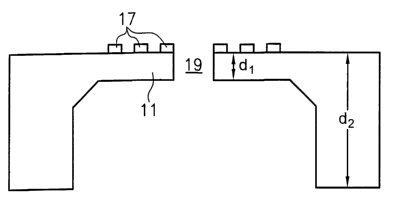
Fig. 1 a and 1 b show a first embodiment 1 of a biochip according to the
present invention.
This biochip comprises a substrate formed with an opening 19 for receiving
therein a cell
membrane which comprises at least one ion channel. In the present case, the
biochip is
shown with M = N = 1.
The substrate comprises a base portion 10 with a first thickness d, and a
window portion 11
with a second thickness d2 in which the opening 19 is provided.
The thickness of the base portion 10 ranges from 1 mm to 100 Nm and the
thickness of the
window portion ranges from 1 pm to 50 nm. The window portion has an area of a
few 10
Nm2 to 0.1 mm2.
CA 02434214 2003-07-07
17
The opening 19 is substantially circular and has a diameter which ranges from
10 pm to 10
nm. The size of the opening is determined by the number of ion channels which
are to be
analyzed in a cell membrane.
The biochip 1 consists of a (0001 ) quartz (Z cut) in which the window portion
11 is first
formed by an anisotropic wet-chemical etch step. The etchant used for this
purpose is HF.
Depending on the size of the desired opening, said opening is formed in the
last step by
optical lithography and a dry-etching step or by electron-beam lithography and
a dry-etching
step.
Furthermore, the surface of the biochip according to Fig. 1 is, in the area of
the opening,
provided with a means for improving the contact between the biochip and the
cell mem-
brane. In the present case, this means is formed by patterning the surface.
For this pur-
pose, annular raised portions 15 are provided, which are arranged around the
opening.
These raised portions have the effect that the membrane with an ion channel to
be ana-
lyzed will be dented, whereby improved adhesion will be achieved due to a
hydraulic effect
and the electrical sealing resistance will be increased.
The patterning in the biochip according to Fig. 1 a and 1 b is only exemplary.
It is especially
also possible to use other forms of raised portions, e.g. one or a plurality
of squares or rec-
tangles, which is or which are arranged around each opening. One of these
alternatives is
shown in Fig. 1 c.
Fig. 2 shows a second embodiment of a biochip according to the present
invention.
Also this biochip comprises a substrate 20, 21 formed With an opening 29 for
receiving
therein a cell membrane which comprises at least one ion channel. Also in the
case of the
biochip shown in Fig. 2, M = N = 1.
The geometrical shape and the dimensions of the biochip 2 correspond to those
of the bio-
chip 1 shown in Fig. 1. In order to avoid repetitions, reference is only made
to the relevant
CA 02434214 2003-07-07
I8
description of Fig. 1 in this connection. The reference numerals of
corresponding parts differ
from one another only with respect to their first figure.
The substrate of the biochip 2 comprises a base portion 20, which is again
made from
quartz, and an etch-stop layer in which the window portion 21 is formed. This
etch-stop
layer consists of Si3NX, preferably of Si3N~.
A characteristic feature of biochip 2, in comparison with biochip 1 of Fig. 1,
is that it can be
produced by a simplified method.
The substrate 20 has first applied thereto an etch-stop film. Subsequently,
the window por-
tion 21 is formed from the opposite side up to said etch-stop layer, said
window portion
being formed by an anisotropic Wet-chemical HF etch step. Finally, the opening
is formed
preferably by one of the methods described in connection with the first
embodiment.
Fig. 3 shows a first embodiment of a biochip 3 according to the present
invention.
With regard to the geometrical dimensions and the structural design, the
biochip 3 essen-
tially corresponds to the structural design of the biochips described in Fig.
1 and 2 so that
reference is here once more made to the description of these chips in order to
avoid repeti-
tions. The reference numerals of corresponding parts differ from one another
only with re-
spect to their first figure.
In contrast to the biochips shown in these figures 1 and 2, the base portion
30 of the sub-
strate consists of a semiconductor material, e.g. (100)-Si.
This semiconductor material has applied thereto an insulating layer in which
the window
portion 31 is formed. The insulating layer 31 additionally serves as an etch-
stop layer in the
production process.
The production process is therefore similar to that of the biochip produced
according to Fig.
2. 1n the embodiment shown, this layer consists of Si3N4.
CA 02434214 2003-07-07
19
In particular, the insulating and etch-stop layer is first applied to the
silicon base portion 30
by means of a PECVD method. Following this, the window portion 31 is formed in
the sub-
strate from the opposite side, said window portion being formed by an
anisotropic wet-
chemical KOH etch step. fn so doing, etching is executed up to the etch-stop
layer. De-
pending on the desired size of the opening, said opening can then be formed,
in a manner
corresponding to the above-described embodiments, by optical lithography or
electron-
beam lithography and a dry-etching step.
In the last step, the electrodes 32 and 33, which consist here of AglAgCl, are
applied to the
upper and to the lower surface of the substrate.
In Fig. 3 it is also shown how a membrane Me with an ion channel I has been
introduced in
the opening 39. For the subsequent measurement, which will be described in
detail with
reference to Fig. 4, an electrolytic liquid 34 must be provided on top of the
membrane and
the electrode 32 as well as in the etch trench.
Fig. 1 to 3 each show biochips with M = N = 1. It goes without saying that the
statements
made hereinbefore also apply to biochips with substrates in which a plurality
of openings is
provided. These openings can be provided in the form of an M x N array. In
such an array
they can be arranged regularly or such that the individual rows are displaced
relative to one
another.
The biochips shown in Fig. 1 to 3 only represent preferred embodiments of the
present in-
vention and should not be regarded as a limitation of said invention.
Hence, a large number of other embodiments, which are not shown, is possible.
It is, for example, not necessary that the opening is circular. It may have
different cross-
sections, depending on the respective requirements to be satisfied.
fn addition, various materials can be used for forming the biochips. It will,
for example, be
possible to use glass instead of the quartz, and, instead of the silicon, a
different semicon-
ductor material, e.g. GaAs, may be used.
CA 02434214 2003-07-07
Especially in the case of a substrate consisting of a semiconductor material,
but not exclu-
sively in the case of such substrates, the surfaces of the substrate may be
coated with a
passivating layer.
Furthermore, different kinds of electrodes can be used, e.g. electrodes which
are suitable
for generating an electromagnetic field in the area of the ion channel.
In addition, electrically and/or optically active and/or passive components
can be integrated
on the substrate.
Likewise, various methods which are known to a sufficient extent from the
field of semicon-
ductor technology can, in dependence upon the respective materials used, be
employed for
producing the biochips.
Fig. 4 shows a measuring probe according to one embodiment of the present
invention.
This measuring probe includes a substrate comprising a base portion 40 and a
window por-
tion 41 in which an opening 49 is formed. In addition, a first electrode 42 is
arranged on the
substrate.
Below the substrate 40, a holding device 45 is secured in position, which is
provided with a
central cavity communicating with the opening 49 and which is followed by an
electrode 43
with a holder.
In addition, the measuring probe comprises a means for generating a vacuum in
the holding
device, said means being designated by reference numeral 46.
in addition to the embodiment of the measuring probe which is shown here and
which
should not be regarded as a limitation of the present invention, further
modifications are
possible.
For example, arbitrary ones of the biochips according to the present invention
can be used
as biochips. In particular the dimensions are then determined by the
respective field of use,
i.e. especially by the number of the channels to be analyzed.
CA 02434214 2003-07-07
21
The holding device may e.g. secured to the substrate by means of an adhesive.
The electrode means including the holder can be implemented such that it can
be screwed
into the holding device from below.
Furthermore, a sealing ring can be provided between the opening of the holding
device and
the electrode that can be screwed in.
In the following, it will be described how ion currents through the ion
channel can be meas-
ured by the present measuring probe.
The cell membrane is first applied to the substrate in an electrolytic
solution. By actuating
the vacuum generating means 46, the membrane including the ion channel is
sucked into
the opening. The measuring probe contains an electrolytic solution 44 as welt.
Finally, the
current flowing through the ion channel can be measured via the two electrodes
42 and 43.