Note: Descriptions are shown in the official language in which they were submitted.
CA 02434516 2003-07-11
WO 02/057738 PCT/IL02/00045
1
NITRIC OXIDE (NO) DETECTOR
Field of the Invention
The present invention relates to nitric oxide (NO) detectors and more
specifically to
an NO detector based on molecular controlled semiconductor resistors.
Background of the Invention
Nitric oxide is one of the most extensively investigated molecules in the f
ells of
inorganic and bioinorganic chemistry. The study of the molecule in biological
systems
received a renewed interest because of its role in a myriad of biological
events. It is probably
correct to state that nitric oxide is involved in practically every common
pathophysiological
event by virtue of its importance in the normal maintenance of many important
physiological
phenomena ranging from the protection of the heart, stimulation and regulation
of brain
functions and vascular tone, to responding to vascular injuries and pulmonary
diseases. The
1998 Nobel Prize in Medicine was awarded jointly to Robert F. Fuchogott,
Louise J. Ignarro
and Ferid Murad for their discoveries concerning "Nitric Oxide as a Signaling
Molecule in
the Cardiovascular System".
The production of NO in the human body proceeds via one of two pathways: an
enzymatic and a nonenzymatic pathway. The enzymatic pathway involves the
action of the
nitric oxide synthases (NOS) on the amino acid arginine with the production of
the
metabolites citrulline and NO. This five-electron oxidation xeaction requires
reduced
pyridine nucleotides, reduced biopteridines and calmodulin. In the
bloodstream, NO binds
primarily to hemoglobin, being then converted to N03- and eliminated in the
urine with a
half life of 5 to 8 hours.
N03- from food and inhaled NO is concentrated in the saliva and converted to
nitrite
by bacteria on the surface of the tongue. When saliva is swallowed, the
nitrite is converted to
NO in the stomach, providing defense against swallowed microorganisms. This NO
production was demonstrated in the stomach, on the surface of the shin, in
infected nitrite-
containing urine and in the ischemic heart (Weitzbarg et al., 1998).
Since the formation of NO is connected with several pathophysiological events,
the
measurement of NO is important for the characterization of important
biological functions
CA 02434516 2003-07-11
WO 02/057738 PCT/IL02/00045
2
during which a change in the measured levels of NO produced may indicate the
existence of
a disease or pathogenesis event. One example for such a phenomena is the
measurable
change in NO production in exhaled air during airway inflammation in asthma
and other
diseases. Measurements of exhaled nitric oxide (ENO) are regarded as a marker
for the
airway inflammations as the concentration of ENO is nearly tripled in the
pathogenesis of
asthma. As exhaled NO is not increased during bronchospasm in the absence of
coexisting
inflammation, it serves to differentiate between the components of asthma and
thereby helps
to direct to the appropriate medication (Hunt et al., 2000; Kissoon et al.,
1999).
In addition to biological events, it is known that oxides of nitrogen (NOX)
originating
from motor vehicles, fossil fuel and power plants are major pollutants that
affect human
health and the ecology. Primary emissions are CO, NO and unburnt hydrocarbons.
It wasn't
until the I990s that NO emissions from cars were recognized as the major cause
of
environmental pollution (Menil et al., 2000). Furthermore, the nitrogen oxides
(N02 or NO)
are a source of ozone, which causes an increase of smog in large cities. This
process, which
occurs via solar irradiation and photolytic decomposition of N02, is a source
of acid rain. At
the same time, NO in the atmosphere reacts with ozone to replenish the
reacting N02, and the
cycle continues.
Monitoring the emission of these pollutants, their transpout in the
atmosphere, and
their degradation to second-generation pollutants is crucial. Direct
monitoring of NO in the
emissions of combustion engines requires a sensor capable of sustaining high
temperatures,
low concentrations of NO (100-1000 ppm) and corrosive medium containing oxygen
and
water vapor. Under these conditions, the nitrogen oxide (NOX) mixtures contain
mainly NO.
The present monitoring techniques of nitrogen oxide mixtures are expensive,
the
measuring devices are bulky and their use is therefore unpractical and
problematic. Efforts
have been concentrated on developing many kinds of NOX sensors such as
electrochemical
sensors which utilize solid electrolytes, thin film superconductor type
sensors, semiconductor
oxide type sensors using Sn02, ZnO, W03, and Ti02 oxide ceramics or thin
films, etc. Using
Sn02 as sensing material, the concentration of gaseous NO was determined to
levels as low
as 10 ppm whereas with solid electrolytes only concentrations in the order of
103 ppm NO
were detectable (l~udo et al., 2000; Becker et al., 2000; Wang et al., 2000).
Nitric oxide (NO) is a small, uncharged, paramagnetic molecule, existing in
gas or
liquid phases. In the gas phase the molecule is stable, compared with a short
half life of
between 5 and 15 seconds measured in biological media. Its diffusion constant
in
physiological medium measured at 3300 ~,m2/s is very similar to that in water.
The solubility
CA 02434516 2003-07-11
WO 02/057738 PCT/IL02/00045
3
of NO in hydrophobic solvents is nine times greater than in aqueous solutions,
which makes
NO an excellent transmitter agent and inflictor of cellular damage, acting
without the
necessity of specific export mechanism such as vascular secretion. NO reacts
with oxygen
species and metals to yield oxidized products such as nitrites and nitrates,
N02 and N03-,
S respectively.
Several methods for detection of NO in solution and in the gas phase have been
developed in recent years for diagnostic or environmental purposes. The fact
that NO is very
reactive in biological tissues makes its direct quantification very complex
and many
measurements, therefore, relied on indirect methods, determining levels of NO
metabolites
such as nitrite and nitrate anions or NO precursors such as citrulline instead
of NO itself.
The most frequently used method to measure the stable nitrite end product is
based on
purple azo dye that was found by Griess more than 100 years ago to recognize
nitrite. In this
method, the nitrite anion binds to N (1-naphthyl)-ethylenediamine (NED) to
produce a purple
dye. Screening the dye-containing solutions by light absorption at 550 mn
produces the
appropriate emission (Schulz et al., 1999). This method does not detect the
second metabolite
of nitric oxide, the nitrate anion N03', thus limiting the detection to only a
fraction of the
volume of NO produced. However, the reduction of the nitrate anion to the
nitrite is usually
achieved using bacterial nitrate reductase or reducing metals such as cadmium.
The detection
limit for the nitrite anion in biological fluids, under the Griess method, is
1.0-1.5 wM (30-45
ppb), with a reaction time of about 20 minutes. A similar method utilizing 2,3-
diaminonaphthalene (DAN) as the nitrite-binding substrate was determined to be
10 times
more sensitive than the conventional technique and at least 50 times more
sensitive for
determining nitrite concentrations in sera or aqueous solutions (Kojima et
al., 2000; Casey et
al 2000).
For directly measuring NO levels in vivo, 1,2-diaminoanthraquinone (DAQ) was
found suitable. It pxoduces a red-fluorescent precipitate when in contact with
NO. This
compound was used to detect changes in NO levels in rat retinas after injury
to the optic
nerve.
In another indirect method, quantification of citrulline instead of NO was
pursued.
However, levels of the amino acid in sera and urine are not good indicators of
NO
production. In cultured cells, the presence of citrulline is primarily due to
NO synthase
enzyme (NOS) activity. Measurements indicated that the citrulline levels were
not
stoichiometrically equivalent to total NO levels as measured by a series of
different methods
(Marzinzig et aL, I997).
CA 02434516 2003-07-11
WO 02/057738 PCT/IL02/00045
4
Other methods for NO identification and quantification include
electrochemical,
fluorescent and transistor-based methods. In one of these methods, the NO is
trapped by
nitroso compounds or reduced hemoglobin forming stable species that can be
quantified by
EPR (electron paramagnetic resonance) with a detection limit of 1 wM (30 ppb).
In another
method NO levels in the gas phase are detected by reaction with ozone,
producing
chemiluminescence, with a detection limit of 20 nM (ppt concentration). Recent
electrochemical methods offer the possibility to measure even lower
concentrations of NO (at
the pM limit) in intact tissues and single cells (Hunt et al., 2000; I~otake
et al., 1999).
Presently existing NO sensors have been manufactured for bedside treatments in
hospitals and medical laboratories for the purposes of treatment and/or
diagnostics. These
sensors are based on the above-mentioned methods of analysis and thus suffer
from several
basic disadvantages such as low S/N ratios, cross sensitivity to other
components in the test
medium, expensive and time-consuming operational steps and inaccurate quantif
canon of
NO or its metabolites due to NO's short half life.
Several methods and devices for measurement of NO in lung conditions, in the
oral
cavity, in the urogenital tract and in the intestines were described in the
United States Patents
US 5,447,165, US 5,922,610, US 6,038,913, US 6,063,027 and US 6,099,480, and
in the
PCT Publications WO 09843539 and WO 09939100.
PTC Publication No. WO 98/19151 (Cahen et al., 1998), of the same applicants
of the
present application, herein incorporated by reference as if herein described
in its entirety,
describes a hybrid organic-inorganic semiconductor device and sensors based
thereon, said
device characterized by being composed of:
(1) at least one layer of a conducting semiconductor;
(2) at least one insulating layer;
(3) a multifunctional organic sensing molecule directly chemisorbed on one of
its
surfaces, said multifunctional organic sensing molecule having at least one
functional group that binds to the said surface of the electronic device, and
at least
one other functional group that serves as a sensor; and
(4) two conducting pads on the top layer making electrical contact with the
electrically conducting layer (1), such that electrical current can flow
between
them at a finite distance from the surface of the device.
These Molecular Controlled Semiconductor Resistors, also designated MOCSER,
are
described in said WO 98/19151 as light or chemical sensors.
CA 02434516 2003-07-11
WO 02/057738 PCT/IL02/00045
Summary of the Invention
It has now been found, according to the present invention, that a device such
as that
described in WO 98/19151 can serve as a sensor for nitric oxide gaseous as
well as dissolved
in biological fluids and in solution, and can specifically detect NO
concentrations in gaseous,
5 biological, and aqueous media.
The present invention thus relates to a semiconductor device (MOCSER) for the
detection of nitric oxide (NO), said device being composed of:
(i) at least one layer of a conducting semiconductor;
(ii) at least one insulating or semi-insulating layer;
IO (iii) a layer of multifunctional organic molecules capable of binding
nitric oxide,
said molecules being directly bound to the surface of an upper layer which is
either a conducting semiconductor layer (i) or an insulating or semi-
insulating
layer (ii); and
(iv) two conducting pads on the upper layer making electrical contact with the
conducting semiconductor layer (i), such that electrical current can flow
between them at a finite distance from the surface of the device.
The multifunctional organic layer (iii) is composed of molecules that can bind
NO
such as, but not being limited to vicinal diarnines, metalloporphyrins,
metallophthalocyanines, and iron-dithiocarbamate complexes. In order to bind
directly to the
surface of the upper layer these molecules should contain at least one
functional group as the
surface binding group (SG) such as, but not being limited to, carboxyl, thiol,
acyclic sulfide,
cyclic disulfide, hydroxamic acid, trichlorosilane or phosphate groups. When
the original
molecule that binds NO does not contain a functional group that binds to the
surface, one or
more desired functional groups can be added to said organic molecules by
methods well
known in the art of chemical synthesis.
Examples of vicinal diamines that bind NO and can be used according to the
invention are, without being limited to, 2,3-diaminonaphthalene, 1,2-
diaminobenzene, 1,2-
diaminoanthraquinone or aminotroponiminate (see Appendix) that are substituted
at the ring
or at one of the amino groups with at least one suitable surface binding group
as defined
above, or the amino group is linked through an aliphatic, aromatic or
araliphatic spacer to
such a surface binding group. Examples of such spacers with their length and
composition
are shown in the Appendix herein, but it is evident to any one skilled in the
art that spacers of
difFerent length and composition can be used according to the invention.
CA 02434516 2003-07-11
WO 02/057738 PCT/IL02/00045
6
Examples of metalloporphyrins and metallophthalocyanines that bind NO and can
be
used according to the invention are, without being limited to, those
containing as central
metal atoms Fe, Co, Ni, Zn, Mn, Cu, Ru, V, Pb or Cr. Many of the natural
porphyrins contain
functional groups such as carboxyl groups on the side chains. For example the
metalloporphyrins derived from hematoporphyrin or protoporphyrin IX (see
Appendix) such
as hematin (ferriprotoporphyrin basic), heme (ferroprotoporphyrin), hemin
(ferriprotoporphyrin chloride) and cobaltic protoporphyrin IX chloride contain
at positions 2
and 1 ~ two propionic acid side chains, namely a carboxyl group linked through
a spacer -
(CHZ)2- in each position. When such functional groups do not exist in the
natural molecule,
desired groups consisting of a spacer terminated with one of the surface-
binding groups can
be inserted at one of the peripheral carbon atoms by methods well known in the
art of
chemical synthesis. The same procedures can be used to prepare suitable
metallophthalocyanines.
The iron-dithiocarbamate complexes that can be used according to the invention
bind
NO through the iron center and to the surface of the device through a surface-
binding group
as mentioned above having a spacer ejected from the nitrogen center. The
spacer may be
aliphatic, aromatic, or a combination thereof, and of varying lengths. The
dithiocarbamate
complex may be symmetric or unsymmetric.
The invention fiu ther relates to an array of semiconductor devices, wherein
each
device in the array is covered with a monolayer consisting of a different NO-
binding
molecule. Said array may optionally further contain other devices carrying
monolayers of
compounds capable to bind to contaminants of NO mixtures such as CO, oxygen,
etc.
In another aspect, the present invention relates to a method for the detection
and
measurement of nitric oxide, which comprises:
(i) exposing a semiconductor device or an array of devices according to the
invention to a sample containing NO; and
(ii) monitoring the presence of NO in the sample and determining its
concentration according to the change in the current measured at a constant
electric potential
applied between the two conducting pads.
The sample containing NO may be gaseous, aqueous or mixtures thereof. In one
embodiment, the sample is a biological fluid such as exhaled air, endogenous
gaseous NO of
the urogenital tract or from the lumen of the intestines. When the sample is
exhaled air, the
method is suitable for evaluating lung conditions for example in asthma
patients.
Measurement of NO from the urogenital tract e.g. from the bladder, urethra,
uterus and
CA 02434516 2003-07-11
WO 02/057738 PCT/IL02/00045
7
oviducts, or from lumen of the intestines, permits to evaluate inflammatory
conditions in
these organs.
Brief Descriution of the Drawings
The present invention will be understood and appreciated more fully from the
following detailed description, taken in conjunction with the examples and
drawings, in
which:
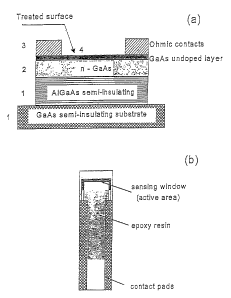
Figs, la-b depict schemes of the MOCSER device of the present invention: la
depicts the layered structure and 1b the layout.
Fig. 2 represents the response of the MOCSER device, covered with a mixed
monolayer of hemin and benzoic acid molecules to various concentrations of NO
dissolved
in physiological media. The insert presents the calibration curve for the
device where the NO
concentration in the media is correlated with the time constant measured.
Figs. 3a-b show measurement of NO produced from brain tissues as measured by a
MOCSER immersed in the artificial cerebrospinal fluid (ACSF) at a distance of
less than 1
mm from the brain slice, in the pxesence (Fig. 3a) and absence (Fig. 3b) of
H202.
Figs. 4a-b demonstrate the sensitivity of the sensor to NO. Fig. 4a depicts
the
response of the device to different concentrations of NO gas in dry air. Fig.
4b presents the
calibration graph obtained both in nitrogen (open circles) and dry air (filled
stars) as a
diluting gas. Insert to Fig. 4b shows the low-concentration range of the
calibration graph
more clearly.
Figs. Sa-b show the reversibility of the device: a) NO dissolved in aqueous
media, b)
NO gas in air.
Fig. 6 shows the sensitivity towards NO as calculated from results.
Figs. 7a-c demonstrate that the effect of exposure of the sensor to gases
other than
NO is minimal. Fig. 7a shows exposures to CO and OZ. Fig 7b and Fig 7c show
the response
of the sensor to NO after pre-exposure to carbon monoxide or oxygen followed
by purging.
Detailed Description of the Invention
According to the present invention, there is provided a device for the
detection of
nitric oxide being a molecular controlled semiconductor resistor, herein
designated
MOCSER, said device being composed of one or more semi-insulating layers, one
conducting semiconductor layer, two conducting pads, and a layer of
multifunctional organic
molecules, characterized by:
CA 02434516 2003-07-11
WO 02/057738 PCT/IL02/00045
8
(i) said conducting semiconductor layer being on top of one of said insulating
or
semi-insulating layers;
(ii) said two conducting pads being on both sides on top of an upper layer
which is
either said conducting semiconductor layer or another of said insulating or
semi-insulating
layers, making electrical contact with said conducting semiconductor layer;
and
(iii) said layer of multifunctional organic molecules consists of molecules
capable of
binding nitric oxide, said molecules being directly bound to the surface of
said upper layer,
between the two conducting pads.
The multifunctional organic molecules that bind NO are molecules such as
vicinal
diamines, metalloporphyrins, metallophthalocyanines, and iron-dithiocarbamate
complexes
that have one or more aliphatic, aromatic or araliphatic side chains
terminated by a functional
group such as carboxyl, thiol, acyclic sulfide, cyclic disulfide, hydroxamic
acid and
trichlorosilane, said functional groups being directly bound to the surface of
said upper
conducting semiconductor layer or insulating or semi-insulating layer.
The device according to the invention serves as an amplifier, which translates
the NO
concentration on its surface into change in the electrical current. Binding of
NO to the
sensing multifunctional molecules results in a change of the charge
distribution, followed by
change in the electrical current, as described previously for different
molecules (Gartsman et
al., 1998; Vilan et al., 1998).
In one embodiment, the semiconductor device of this invention is composed of
one or
more insulating or semi-insulating layers (1), one conducting semiconductor
layer (2), two
conducting pads (3), and a layer of at least one capable of binding NO (4),
characterized in
that: said conducting semiconductor layer (2) is on top of one of said
insulating or semi-
insulating layers (1), said two conducting pads (3) are on both sides on top
of an upper layer
which is either said conducting semiconductor layer (2) or another of said
insulating or semi-
insulating layers (1), making electrical contact with said conducting
semiconductor layer (2),
and said layer made of at least one compound capable of binding NO is adsorbed
on the
surface of said upper layer, between the two conducting pads (3).
The semiconductor of layer (2) of a MOCSER of the invention may be a
semiconductor selected from a III-V and II-VI material, or mixtures thereof,
wherein III, V,
II and VI denote the Periodic Table elements III=Ga, In; V=As, P; II=Cd, Zn;
VI=S, Se, Te.
In preferred embodiments, the conducting semiconductor layer (2) is a doped n-
GaAs or
doped n-(AI,Ga)As, doped preferably with Si.
CA 02434516 2003-07-11
WO 02/057738 PCT/IL02/00045
9
In another embodiment, the one or more insulating or semi-insulating layers
(1) of a
device of the invention, that may serve as the base for the device, is a
dielectric material
selected from silicon oxide, silicon nitride or from an undoped semiconductor
selected from a
III-V and a II-VI material, or mixtures thereof, wherein III, V, II and VI
denote the Periodic
Table elements III=Ga, In; V=As, P; II=Cd, Zn; VI=S, Se, Te and is preferably
undoped
GaAs or (AI,Ga)As substrate.
In one preferred embodiment, the MOCSER of the invention is based on a
GaAs/(AI,Ga)As structure. According to this preferred embodiment, there is
provided a
MOCSER wherein said conducting semiconductor layer (2) of doped n-GaAs is on
top of a
semi-insulating layer (1) of (AI,Ga)As which is on top of another semi-
insulating layer (1) of
GaAs, and on top of said conducting semiconductor doped n-GaAs layer (2) there
is a semi-
insulating undoped GaAs layer (1) to which is attached said layer of at least
one compound
capable of binding NO (4).
A MOCSER according to the invention was developed as disclosed in WO 98/19151
as a multilayered GaAs based device as depicted in Fig. 1 which contains a
conducting n-
doped GaAs upper layer (active layer of 450-500, doped to concentration of 4-
7E17 cm 3)
that is close to the surface. This active layer lies between semi-insulating
layers, e.g. an
undoped semi-insulating uppermost GaAs layer (50-100 A) and a semi-insulating
AlGaAs
layer (of 1500-4000 A) above a GaAs semi-insulating substrate, connected to
two ohmic
contacts, e.g. AuGeNi. The MOCSER will preferably be rinsed in organic
solvents and
treated in ozone cleaning system prior to use.
According to this same preferred embodiment, there is further provided a
MOCSER
wherein said conducting semiconductor layer (2) of doped n-(AI,Ga)As is on top
of an
insulating layer (1) of undoped GaAs which is on top of a semi-insulating
layer (1) of GaAs,
on top of said conducting semiconductor doped n-(AI,Ga)As layer (2) there is a
semi-
insulating undoped (AI,Ga)As layer (1) on top of which there is an upper
undoped GaAs
semi-insulating layer (1), and said monolayer of at least one compound capable
of binding
nitric oxide (4) is attached to the upper undoped GaAs semi-insulating layer
(1).
The sensing metalloporphyrin or other similar organic compound capable of
binding
NO making-up the monolayer will vary according to the purpose of the detection
and the
medium or environment in which the nitric oxide is to be tested.
Examples of the various applications of the MOCSER as a sensor for nitric
oxide,
without being limited to: (1) detection of NO in exhaled air for monitoring
asthma and/or
other airway inflammation and/or gastric activity; (2) detection of NO in
polluted air; (3) ih-
CA 02434516 2003-07-11
WO 02/057738 PCT/IL02/00045
vitro detection of NO in various physiological media, resulting from NO-
producing living
cells; (4) in-vivo detection of NO in physiological medium and in living
cells, for the purpose
of measuring metabolic activity, and/or toxicity, and for the diagnosis of
heart diseases,
circulatory shock and cancer.
5 The invention also relates to an array of semiconductor devices (MOCSERs) as
described above, wherein at least one device contains the NO-binding compound
and at least
one of the remaining devices in the array is adsorbed with a different
selective organic
molecule which selectively binds contaminants present along with the nitric
oxide in the
tested medium. Examples of such contaminants are carbon monoxide, oxygen,
inorganic salts
10 and other organic and inorganic molecules present in exhaled air, bodily
fluids, biological
solutions and other media. These molecules are well known in the art.
In one preferred embodiment, at least one of said MOCSERs in the array is
covered
with a monolayer of molecules that bind NO and at least one of the other
devices contains a
molecule that binds selectively the contaminating species, e.g. CO and/or 02.
The response
of each individual MOCSER is measured, recorded and then processed to extract
the signal
produced by the NO-binding molecules.
According to the present invention, a device for detection of Nitric Oxide
(NO) is
provided that is based on a MOCSER structure, preferably of a GaAs/(AIGa)As
device,
where on top of one of its surfaces a monolayer of NO-binding organic
molecules is
adsorbed. A current flows through the device when voltage is applied between
its two
electrodes. When the adsorbed monolayer of NO-binding molecules interacts with
NO
molecules, present in the tested medium, the charge distribution in the
binding molecules
changes. The change in the charge distribution affects the current flowing
through the device.
The concentration of the NO in the medium can be monitored as correlated from
the
electronic response of the device: the higher the NO concentration, the
faster/higher is the
observed change in the MOCSER's current.
This invention will be fully appreciated from the following detailed
description and
examples taken in conjunction with the drawings.
Fig. 1 depicts schematically an NO detector according to this invention based
on a
field effect transistor (FET) in which two electrodes are used. This FET-like
device structure
has a semi-insulating, undoped buffer (AI,Ga)As layer (1) on top of a semi-
insulating GaAs
substrate (1), a thin layer of conducting semiconductor n-GaAs (2) (the active
layer) on top
of the semi-insulating (AI,Ga)As layer (1), a protective upper thin layer of
undoped semi-
insulating GaAs layer (1) covering the conducting semiconductor n-GaAs layer
(2), and a
CA 02434516 2003-07-11
WO 02/057738 PCT/IL02/00045
11
monolayer (4) of a NO-binding compound such as a metalloporphyrin adsorbed on
the
undoped GaAs surface (1). Two conducting AuGeNi electrodes (3) serve as
electric contacts.
These are the two olnnic contacts- source and drain, connected to the n-doped
GaAs active
layer that lies between the semi-insulating layers.
This molecular controlled semiconductor resistor (MOCSER) is highly sensitive
to
chemical changes on its surface. The molecules that are adsorbed on the Ga,As
surface
change the surface potential, which affects the resistance of the MOCSER. The
MOCSER
also has a short response-time (Vilan et al., 1998) and its operation is very
simple.
The detection of nitric oxide (NO) and its quantification is a very important
tool in
the diagnosis of diseases and environmental pollution.
The measured binding (affinity) constants of NO to the metallic heme centers
reflects
the stronger interactions of the NO group as compared with that of CO. Direct
addition of
NO gas or of an aqueous solution of NO to metalloporphyrins or heme appears to
be the most
widely used method for the preparation of nitrosyl metalloporphyrins or
nitrosyl-hemes.
These have been studied extensively in past years as better understanding of
the vital role of
NO in mammalian life was realized.
In one preferred embodiment of the invention, the NO-binding compound is a
metallopozphyrin. The combination of the sensitivity of the MOCSER and the
affinity of the
organic metalloporphyrins layer towards the NO molecule, with high selectivity
as compared
with carbon monoxide, carbon dioxide, nitrogen dioxide, oxygen, nitrogen and
water are the
basic principles behind the present invention. The greater affinity of the
metalloporphyrins-
covered MOCSER to NO as compared to the contaminating species such as CO,
allows the
detection of NO in complex mixtures such as exhaled air. As a result of the
reaction between
the monolayer of metalloporphyrins and the NO molecules, producing a monolayer
of
nitrosyl porphyrins, a small change in the conductivity of the MOCSER will be
induced. The
changes in the current should vary with varying NO concentrations.
The invention will be further illustrated by the following non-limiting
examples.
Examples
Example 1. General Method of Preparation
The electronic properties of semiconductor devices are strongly affected by
the
properties of the surface, which can be modified by adsorbed molecules. The
interaction
between the adsorbate and the substrate causes shift of the electron density
to or from the
CA 02434516 2003-07-11
WO 02/057738 PCT/IL02/00045
12
surface, depending on the position of the energy state in the adsorbate and
the substrate.
Thus, the surface charge density and distribution can be changed by the
adsorbates, and the
effect of the adsorption can be determined.
GaAs is a III-V compound semiconductor with a direct band-gap of 1.42 V. In
the
experiments herein, GaAs (100) surface was used and the monolayer of the
metalloporphyrins was adsorbed on its surface. The adsorption process is
monitored using
Fourier Transform Infra Red Spectroscopy (FTIR) and X-ray photoelectron
Spectroscopy
(XPS). As was described above, the metalloporphyrins used have several
vibrational bands
that are active in the FTIR measurement. The main features axe: (1) carbonyl
groups, as
described above, (2) C=C and C=N bonds from the porphyrin cycle and the
exocyclic double
bonds, (3) the vibrations arising from the macrocyclic porphyrin system and
(4) alkyl
substituents.
Organic molecules can be chemically adsorbed on the surface of the GaAs device
via
several functional groups: phosphates, carboxylic acids, disulfides, thiols,
and hydroxamic
acids. The best binders are the phosphate and the carboxylic acids,
demonstrating irreversible
binding under a vast spectrum of conditions. Binding the sensor molecules via
a two-site
dicarboxylate results in the greater strength of the bonding as compared with
sulfides or
monocarboxylates. According to the invention we utilized as a non-limiting
example
naturally occurring porphyrins such as hemin that have two free carboxylic
acid groups for
illustration of the concept of the invention.
The adsorption of organic compounds having more than one carboxylic acid group
proceeds via initial binding of one of the groups and formation of a Ga-
carboxylate bond,
followed by the adsorption of the second group in the same fashion. At times
when the
binding domains are in close proximity to each other, the adsorption of the
second group may
be ineffective because of steric reasons. Differentiation between the two-step
adsorption
process of dicarboxylic acids and the adsorption process of a single
carboxylic acid group
was confirmed using both FTIR and electronic measurements.
The IR absorption spectrum of the unbound organic ligand containing a
dicarboxylic
acid functionality may exhibit peaks corresponding to the syrmnetric
stretching of both
carboxylic groups and unsymmetrical stretching that arise from the
unequivalent stretching
of each group relative to the other. Furthermore, in cases where hydrogen
bonding between
the carboxylic acid groups is possible, noticeable shifts of the peaks will
hint to that. In the
IR spectrum of hemin porphyrins the dicarboxylic acid functionality gives rise
to a strong
and broad band at 1747 cm 1, arising from both the symmetric and unsymmetric
vibrations of
CA 02434516 2003-07-11
WO 02/057738 PCT/IL02/00045
13
the two free carboxylic acid groups. The frequency of this band does not
attest to any
intramolecular hydrogen bonding that may be at play in this molecule.
In the case of a two-step adsorption onto the GaAs surface, two different IR
spectra
are obtained; one taken 0.5-5 hours after the beginning of the adsorption and
the second
taken 12 hours thereafter. The differences in the spectra arise from the
incomplete adsorption
of the dicarboxylic acid functionality to the surface. Four hours after the
adsorption begins,
only one carboxylic acid ("arm") is bound to the surface, which is attested to
in the IR
spectrum by the presence of one carboxylic acid band at around 1740 cm 1 and
one Ga-
carboxylate band whose frequency is shifted to around 1700 cm 1. The
adsorption of the
second arm to the GaAs surface requires a longer adsorption time and is
observed to end with
the nearly complete disappearance of the band at 1740 cm 1 and the
strengthening of the 1700
cm 1 band. If steric interactions are not overcome during the longer
adsorption times, some
bands corresponding to the free carboxylic acid arms may still be present in
the IR spectrum.
The MOCSER covered with a monolayer of the metalloporphyrins is introduced
into
the medium containing nitric oxide molecules. The NO molecules thus bind to
the metal
centers of the porphyrin monolayer, effecting a change in the electric charge
distribution on
the surface of the MOCSER. The changes of the current in time are monitored at
a constant
voltage.
The selectivity of the system towards nitric oxide is evident from the
reaction of the
metalloporphyrins covered MOCSER with various molecules such as carbon
monoxide,
carbon dioxide, nitrogen dioxide, oxygen, nitrogen, and water (not shown). The
magnitude
and the time constant of the change in the current through the MOCSER during
exposure to
one of the above contaminants is different from the changes in the current
during exposure to
nitric oxide.
Example 2. Adsorption of the metalloporphyrins onto the MOCSER
Prior to each adsorption, the GaAs surface of the device is cleaned by boiling
in
trichloroethylene, acetone and absolute ethanol for 15 minutes, consecutively,
etched for ten
seconds in a 1:9 NH3/H20 (v/v) solution, washed with de-ionized water and
dried under a
stream of nitrogen (99.999%). The MOCSERS are then immersed in DMF or CH3CN
solutions containing one of the metalloporphyrins (maximum concentration of 15
mM), for a
period allowing maximal adsorption. The devices are next rinsed with 5%
chloroform/hexane
and blown dry under a stream of nitrogen gas.
CA 02434516 2003-07-11
WO 02/057738 PCT/IL02/00045
14
In an alternative method, after the etching the MOCSERs are immersed in a 1:1
solution of the metalloporphyrins and benzoic acid. This is done in order to
avoid the
possible ~-~ electronic interactions between neighboring porphyrins.
The mixed monolayers are characterized by FTIR using bare, etched, and
oxidized
GaAs surfaces, as references. The adsorption of the mixed monolayer onto the
GaAs results
in the appearance of a strong peak at 1710 cm 1 (v~~oo of porphyrin), while
the peaks which
are indicative of the free carboxylic acid groups of both the porphyrin and
the benzoic acid,
at 1747 and 1675 cm 1, respectively, disappear. This indicates that the
carboxyl groups bind
to the GaAs surface, with a film thickness of about one monolayer (Wu et al.,
2000).
AFM images of the mixed monolayer formed indicate that the thickness of the
monolayer is about 1.5-1.7 nm, a thickness that is comparable with a monolayer
of
porphyrins bound through the carboxyl groups and not via stacking.
Furthermore, AFM
studies indicate that the presence of the benzoic acid molecules assist in
forming a more
"ventilated" porphyrin monolayer to which the NO approach is facilitated (Wu
et al., 2000).
Example 3. The Measurements
The device response to NO was evaluated at room temperature under anaerobic
and
aerobic conditions without effecting oxidation of the nitric oxide to the more
stable nitrite
and nitrate ions.
3.1 Measuring NO Concentrations using NO-Releasing Precursors.
During the experiment, a constant voltage of 100 mV is applied between the
ohmic
contacts of the MOCSER. The change in the current vs. time, I (t), is
monitored in a buffer
solution (pH=7.4), while the nitric oxide is released from a precursor such as
1-hydroxy-3-
methyl-3-(methylaminopropyl)-2-oxo-1-triazene (tli2=10.1 minutes), or other
similar triazene
compound, at a controllable rate.
The response of the bare device to high concentrations of nitric oxide is
shown in Fig.
2, which represents the response of a typical porphyrin-covered MOCSER to the
NO
released. The current of the device slightly decreases as compared with the
observed increase
as a response to the reaction of the nitric oxide with the organic ligand. In
addition, unlike the
concentration-dependant response observed with the porphyrin-covered device,
the response
observed with the bare MOCSER is, to a certain extent, concentration
independent. From
Fig. 2 it is clear that the device's response to the NO produced is rapid, the
response is very
stable, and current saturation occurs in less than 10 minutes.
CA 02434516 2003-07-11
WO 02/057738 PCT/IL02/00045
Several additional experiments indicate that the response of the MOCSER to NO
results solely from the interaction of the organic monolayer with varying
concentrations of
NO, and that there was no measurable response to the following: 1) solutions
of the NO-
releasing precursors prepared under conditions such that the NO molecules are
not produced;
5 2) buffer solutions (pH=7.4) containing none of the NO precursor; 3)
solutions at pH=10-11;
4) solutions of the metabolites produced from the NO-producing precursors
(diamines); and
5) porphyrin systems containing no metal center.
3.2 Measuring NO in Hippocampal Slices in Artificial Cerebral Spinal Fluid
10 (ACSF).
Brain slices of rat or guinea pig release NO after depolarization induced by
high
potassium or after electrical stimulation of the slice, but the production of
H202 is
unavoidable. The response of the bare MOCSER to hydrogen peroxide arises from
the
oxidation of the device's surface. However, when the surface of the MOCSER is
covered
15 with a monolayer of organic compounds, the reactivity of the GaAs surface
reduces
dramatically. A differentiation between the response towards the hydrogen
peroxide and the
nitric oxide both evolved in the process of brain cell stimulation is possible
due to the
successful protection of the GaAs surface by the porphyrin monolayer.
The measurements were performed in the presence and absence of 20 ~,M of
hydrogen peroxide. Electrical stimulation of the brain slices (one-second
train of pulses at a
rate of 100Hz) was started after the MOCSER was in prolonged and continuous
contact with
the slice and the media, and after signal stabilization (base line). Figs. 3a-
3b show
measurements of NO produced by brain tissues as measured by a MOCSER immersed
in the
artificial cerebrospinal fluid (ACSF) at a distance of less than 1 mm from the
brain slice, in
the presence (fig. 3a) and absence (Fig. 3b) of H202.
As Figs. 3a and 3b show, the MOCSER immersed in the ACSF, at a distance of
less
than 1 mm from the brain slice, showed no detectable response towards hydrogen
peroxide
prior to or after electrical stimulation. The response observed arises solely
from the evolution
of NO. There is an increase of the current as a result of the slice
stimulation.
Two parameters were extracted from each of the measurements: the amplitude,
dI, of
the current change (difference between the current saturation and the initial
current prior to
stimulation) and the time constant, i, characterizing the rate of the NO
binding to the
MOCSER. The observed values of DI are 30-80 nA which correspond to a
concentration of
several ~,M of NO.
CA 02434516 2003-07-11
WO 02/057738 PCT/IL02/00045
16
In these measurements, the release of NO from the brain slices depends on the
response to the electrical stimulation. This allows a supply of NO to the
media in one batch
and without further replenishment. With measurements utilizing the NO-
releasing precursors
(see above), the time constant is controlled by the rate at which the NO is
released from the
organic precursors. In the brain slices measurements i is dependent on the NO
decomposition
process; meaning on its half life. Therefore, the two time constants namely,
of NO released
from brain slices and of NO released from the NO-releasing precursors, are not
comparable
and do not define an identical process. The processes that bring about the NO-
porphyrin
binding are fast relative to the other processes and can thus be neglected. In
fact, the
observed i values are 12-13 seconds, which correspond nicely with the reported
nitric oxide
half life of about 5-15 seconds.
3.3 Measuring Gaseous NO Concentrations.
Gas mixtures of NO in nitrogen gas or, alternatively, in dry air (containing
79
nitrogen, 21 % oxygen, 530 ppm C02, 5 ppm CO and <6 ppm H20) were prepaxed in
various
concentrations, varying from 5 ppb to 10 ppm NO in N2 or air, using a Multi-
Gas Calibrator.
Each gas mixture was brought in contact with the MOCSER at a constant flow,
temperature
and under controlled consistent conditions. A constant voltage of 100 mV was
applied to the
MOCSER and a current flowing through the MOCSER was monitored using a Source-
Measuring Unit.
The sensitivity of the sensors, covered by a monolayer of Cobaltic
Protoporphyrin IX,
to the NO is shown in Fig. 4a. The varying concentrations produced consistent
and reliable
responses that allowed facile differentiation of NO concentrations. As can be
seen from Fig.
4a, the electrical current decreased significantly when the sensor was exposed
to NO. The
response of the device depended on the concentration of NO and its
reproducibility in a
constant concentration of NO was excellent as tested on a single device or on
different ones.
Both the saturation value of the current change 0I = (Isar°ratioa Io)
~d the rate of the current
change ~~ correlate with the NO concentration (Fig. 4a), therefore, both
parameters can be
used for the sensor calibration. The calibration curve shown in Fig. 4b
presents the
dependence of ~t on the NO concentration in the range 0-700 ppb both in
nitrogen (shown
by open circles) and in dry air (shown by stars) for MOCSERs, covered by a
monolayer of
Cobaltic Protoporphyrin IX. There is no significant difference between the
calibration curves
CA 02434516 2003-07-11
WO 02/057738 PCT/IL02/00045
17
obtained in nitrogen and in dry air that demonstrates that the sensitivity of
the sensor to NO
is not influenced by the presence of oxygen, C02 and CO.
Only a weak, almost concentration-independent, response of the MOCSER to NO
was observed in the absence of the organic porphyrin or the organic porphyrin-
benzoic acid
mixed monolayer that confirmed that NO interactions were with the organic
monolayer that,
in turn, influenced the GaAs surface.
Example 4. Reversibility of the NO Sensor
The reversibility and usability of the MOCSER as a sensor for nitric oxide was
demonstrated in both the aqueous and gas phases. Over a cycle of several
measurements the
sensor was exposed to the NO-containing medium (gas or solution), taken out
and purged
with nitrogen gas or dry air and measured again. In aqueous solution, the
saturated current
relative to the original change are 1:0.74:0.57:0.44:0.31 (Fig. 5a),
demonstrating a reasonable
reversibility of the system. The decrease of the saturated current upon
repeated cycling
indicates that the porphyrin layer is either slowly oxidized or damaged. In
gas mixtures (Fig.
5b), the effect of the deterioration of the sensor sensitivity was much
weaker, demonstrating
the same rates (18 ~ 2 pA/sec) of the change in the current over a cycle of
several
measurements. From Fig. 5b it is cleax that the device can be regenerated for
further and
continuous use by nitrogen gas or dry air purge profile. The purging period
results in a
complete regeneration of the response once the same device was re-exposed to
the sane NO
concentration. In addition, exposing the NO-bound layer to a short laser pulse
(50 ns, 532
nm) regenerates the NO-free monolayer.
Exam~ele 5. Sensitivity of the Device to Nitric Oxide
5.1 Licruid phase
From Fig. 6 it is apparent that the device is highly sensitive to NO produced
ivc vitro
and that response is quite rapid. From direct measurements it was found that
the device is
sensitive to concentrations as low as 1.3 ~.M (39 ppb; 1 ~,M = 30 ppb NO) in
solution. It is
also worth of noting that the response time of the current is different at
different NO
concentrations. This is shown in Fig. 2: when the current reaches "steady-
state" the response
time is about 5, 10, and 20 minutes for concentrations of 16, 6.7, and 2.6 ~.M
(480, 210 and
78 ppb) of NO-releasing solution, respectively.
CA 02434516 2003-07-11
WO 02/057738 PCT/IL02/00045
18
In order to understand the sensitivity of the device, the concentration of NO
was
measured at different times (from Fig. 6) using the equation:
[NO] ~ Co(1-a is X io-3t)
where [NO] is the concentration of NO at time, t (sec), and Co is the total
concentration of the
NO adduct in the buffer solution. The relationship between the current and the
concentration
that is obtained is shown in Fig. 6. From this, it can be concluded that the
device can respond
to NO concentrations of as low as 0.7 ~,M.
Experimentally, we find a correlation for the change in the current upon
introduction
of the NO medium over a certain time range. From the known variables t and Co,
we can
calculate the exact concentration of NO at any time for which the linear
correlation holds
(Wu et al., 2000).
5.2 Gaseous phase
Fig. 4 demonstrates the directly measured responses of the sensor to the NO
concentrations down to 10 ppb. The response is quite rapid: the period of 10-
20 sec is enough
in order to distinguish between the responses to different NO concentrations
and to calculate
the rate of the current change, ~~ , accurately. It is clear from the response
of the sensor to
the concentration of 10 ppb that the signal-to-noise ratio is rather good and
allows
determination of even lower concentrations of NO.
Example 6. Calibration of the Deyice to NO
The device is calibrated to report accurate concentrations of NO in the
examined
media. The calibration curves utilized are based on series of measurements of
varying
concentrations of NO. Each media produces a different calibration curve, as
can be seen in
the inserts of Figs. 2 and 4.
Example 7. Sensitiyity and Selectivity of the NO Sensor for other substances
As was shown earlier, the response of the device in a medium containing NO
stems
solely from interactions between the porphyrin monolayer and the NO present.
Experiments
with each component of the various media or various mixtures thereof resulted
in no
response from the device. In this aspect, the bare MOCSER or the MOCSER
covered with a
CA 02434516 2003-07-11
WO 02/057738 PCT/IL02/00045
19
monolayer of porphyrin molecules exhibited no detectable response to water,
buffer solutions
over a range of pH values, to solutions of free amines and ammonium salts, or
to NO-
releasing compounds or their metabolites (not shown).
Fig. 7 demonstrates the selectivity of the NO sensor towards gaseous
substances. As
can be seen from the Fig. 7a the response of the device towards 10 ppm carbon
monoxide in
nitrogen and 1 % carbon dioxide in nitrogen is minor. Although the response of
the sensor
towards 10 % oxygen in nitrogen is significant, the comparability of the NO
calibration
curves, obtained with nitrogen or dry air (containing 21 % oxygen) as a
diluting gas (see
Fig. 4b), proves that the sensitivity of the sensor to NO is not affected by
the presence of
oxygen. There is no detectable response of the sensor to other inert gases.
Pre-exposition of the sensor to different gases before the exposure to NO does
not
affect the sensitivity of the sensor towards NO. As can be seen from the Fig.
7b and Fig. 7c,
the response of the sensor, exposed to 10 ppm carbon monoxide or 10 % oxygen
and purged
with nitrogen or dry air afterwards, is similax to that of a non-used device.
That proves the
high selectivity of the organic monolayer towards NO in presence of much
higher
concentrations of different gases.
Example 8. Contact Potential Difference (CPDI Measurements
Kelvin probe measurements were performed in order to study the effects of the
adsorbed porphyrin molecules on the device's electronic properties. The 1:1
mixture of
porphyrin and benzoic acid was adsorbed on the GaAs surface of the MOCSER, as
was
described earlier, and the contact potential difference (CPD) between the n-
GaAs surface and
the Au grid was measured by a Kelvin probe in ambient.
The effective electron affinity (~ was found to increase as a result of the
porphyrin
adsorption onto the GaAs surface, which also caused a decrease in the band
bending (VS) of
the sample studied (not shown). For example, for baxe n-GaAs x = 4.4~0.5 V and
VS =
350~40 mV, while after adsorption of the porphyrin x = 4.6~0.2 V and VS =
320~80 mV.
This change indicates that the dipole of the adsorbed molecules is oriented
with the negative
pole pointing away from the surface with a minor decrease of the net surface
charge.
CA 02434516 2003-07-11
WO 02/057738 PCT/IL02/00045
Discussion
Nitric Oxide (NO) is recognized as playing a crucial role in a vast number of
functions in mammalian life. The basic requirement for the development of a
diagnostic tool
5 for measuring NO is the development of a cheap and reliable sensor.
According to the invention we showed that the MOCSER in its current embodiment
could be successfully used as a sensor for the detection of nitric oxide in
biological media, in
gas mixtures and in aqueous media. The sensitivity of the device described
here towards NO
is independent of other species present in the tested medium. Furthermore,
unlike other NO
10 sensors described in the literature, the device based on MOCSER is easy and
cheap to
manufacture, manipulate, and operate.
On the basis of the IR spectra it is clear that a sufficient monolayer of
porphyrin
molecules is formed on the surface of the GaAs based device. The binding that
occurs via a
set of two carboxylic acid groups is achieved in a homogeneous solution of the
porphyrin in
15 DMF. The binding and stability were monitored and studied by FTIR, XPS and
CPD
measurements.
With the presented device, three different media containing varying NO
concentrations were examined. The different threshold sensitivity to low
concentrations of
NO observed for the three media arises from the dynamics of the NO approach to
the sensor
20 molecules.
In solution media concentrations of as low as 30 ppb NO are detected in the
presence
of other dissolved organic and inorganic compounds, such as hydrogen peroxide,
free
amines, ammonium salts, hydrocarbons, and dissolved gases. In gaseous media,
concentrations of as low as 10 ppb were detected with selectivity of several
orders of
magnitude towards other gases. This unique selectivity of the porphyrin layer
and even more
importantly the ability of the device to electrically distinguish between
various species give
the sensor of the invention its powerful characteristics.
Reusability of the sensor is another aspect that is of importance. The MOCSER
device may be reused over time by simply purging the surface of the device
with nitrogen gas
or dry air. The devices are stable in inert atmosphere and at room temperature
for long
periods of time (several months). This is important for the construction of
sensors that can be
stored for long periods of time.
All of the above mentioned characteristics of the sensor device afford a
system with
manifold potential applications.
CA 02434516 2003-07-11
WO 02/057738 PCT/IL02/00045
21
References
Becker Th., Muhlberger St., Braunmuhl Chr. Bosch-v., Muller G., Ziemann Th.,
Hechtenberg K. V., " Air pollution Monitoring Using Tin-Oxide Based
Microreactor
Systems", Sensors and Actuators B, 69, 108-119 (2000).
Casey T. E., Hilderman R. H., "Modification of the Cadmium Reduction Assay for
Detection
of Nitrite Production Using Fluorescence Indicator 2,3-Diaminonaphthalene",
Nitric Oxide:
Biology and Chemistry, 4, 67-74 (2000).
Gartsman K., Cahen D., Kadyshevitch A., Libman J., Moav T., Naaman R., Shanzer
A.,
Umansky V., Vilan A., "Molecular Control of a GaAs Transistor", Chem. Phys.
Lett., 283,
301 (1998).
Hunt J., Gaston B., "Airway Nitrogen Oxide Measurements in Asthma and Other
Pediatric
Respiratory Diseases", J. Pediatr., 137, 14-20 (2000).
Kissoon N., Duckworth L., Blake K., Murphy S., Silkoff P. E., "Exhaled Nitric
Oxide
Measurements in Childhood Asthma: Techniques and Interpretation", Ped. Pulm.,
28, 282-
296 (1999).
Kojima H, Nagano T., "Fluorescent Indicators for Nitric Oxide", Adv. Mater.,
12, 763-765
(2000).
Kotake Y., Moore D R., Sang H., Reinke L. A., "Continuous Monitoring of in
Vivo Nitric
Oxide Formation Using EPR Analysis in Biliary Flow", Nitric Oxide: Biology and
Chemistry, 3, 114-122 (1999).
Kudo M., Kosaka T., Takahashi Y., Kokusen H., Sotani N., Hasegawa S., "Sensing
Functions to NO and 02 of Nb205- or Ta205-Loaded Ti02 and Zn0", Sensors and
Actuators
B, 69, 10-15 (2000).
Marzinzig M, Nussler A. K, Stadler J, Marzinzig E, Barthlen W, Nussler N. C,
Beger H. G,
Moris S. M, Bruckner U. B., "Improved Methods to Measure End Products of
Nitric Oxide in
CA 02434516 2003-07-11
WO 02/057738 PCT/IL02/00045
22
Biological Fluids: Nitrite, Nitrate, and S-Nitrosothiols", Nitric Oxide:
Biology aad
Chemistry, l, 177-189 (1997).
Menil F., Coillard V., Lucat C., "Critical Review of nitrogen Monoxide Sensors
for exhaust
Gases of Lean Burn Engines", Sensors and Actuators B, 67, 1-23, (2000).
Schulz K., Kerber S., Kelm M., "Reevaluation of the Griess Method for
determining
NO/NOZ in Aqueous and Protein-Containing Samples", Nitric Oxide: Biology arcd
ChenZistry, 3, 225-234 (1999).
Vilan A., Ussyshkin V. R., Gartsman K., Cahen D., Naaman R., Shanzer A., "Real
Time
Monitoring of Adsorption Kinetics: Evidence for 2-site Adsorption Mechanism of
Dicarboxylic Acids on GaAs (100)", J. Phys. Chem. (B),102, 3307-3309 (1998).
Wang X., Miura N., Yamazoe N., "Study of W03-Based Sensing Materials for NH3
and NO
Detection", Sensors and Actuators B, 66, 74-76 (2000).
Weitzbarg E. Lundberg J. O. N., "Nonenzymatic Nitric Oxide Production in
Humans", Nitric
Oxide: Biology and Chemistry, 2, 1-7 (1998).
Wu D. G., Ashlcenasy G., Shvarts D., Ussyshkin V. R., Naaman R., Shanzer A.,
Cahen D.,
"Novel NO Biosensor, Based on Surface Derivatization of GaAs by 'Hinged' Iron-
Porphyrins", Angew. ChenZ., Int. Ed. Ercgl., 39 (24), 4496-4500 (2000).
Wu D. G., Cahen D., Graf P., Naaman R., Shanzer A., Shvarts D., "Direct
Detection of Low
Concentration NO in a Physiological Solutions by a New GaAs Based Sensor",
Chem. Eur.
J., 7(8), 1743-1749 (2001).
CA 02434516 2003-07-11
WO 02/057738 PCT/IL02/00045
23
APPENDIX: Structures of NO-binding molecules
I. Metalloporphyrins
OH
H v v ~0 HO U a H
Hematoporphyrin IX Protoporphyrin IX
35
HO' \\O p OH HO O O OH
Hemin 40 Cobaltic Protoporphyrin II Chloride
50
CA 02434516 2003-07-11
WO 02/057738 PCT/IL02/00045
24
II. Vicinal diamines
\ NHz \ \ NHa
NH I
~ / ~
NH
S acerJ
SG' Spacer p ~ Spacer
SG SG
aminotroponiminate 1,2-diaminobenzene 2,3-diaminonaphthalene
derivatives derivatives derivatives
N ~ \Fe N
i ~i~~~ ~
Spacers S-S Spacer
SG SG
Iron-dithiocarbamate
SG= a surface binding group such as carboxyl, thiol, acyclic sulfide, cyclic
disulfide,hydroxamic acid, trichlorosilane or a phosphate group.
Spacers: -(CH2)" or -(CH2)m / \ (CHz)m
n=0-5, m=0-2.