Note: Descriptions are shown in the official language in which they were submitted.
CA 02434622 2006-07-06
29903-137
1
T1/E1 FRAMER ARRAY
BACKGROUND OF THE INVENTION
FIELD OF THE INVENTION
The present invention relates to frame detection
and generation and, more particularly, to processing
multiple independently-clocked data streams.
DESCRIPTION OF THE RELATED ART
Digital data transmission systems include
facilities for frame detection and frame generation. In
general, there are two approaches in the prior art for
processing the individual data streams.
In a first conventional method, the frame
detection and frame generation facilities are placed in
directly in each data path in order to preserve the timing
of the individual data streams. However, this requires
replication of facilities and requires multiple, independent
clock domains.
Another conventional approach uses state machine
logic to handle multiple data streams by preserving the
state of individual data streams in static RAM (random
access memory). As used herein "state" or "context" of data
streams refers to system register settings of a particular
data stream. Each stream is typically processed as follows:
(a) the prior state of the state machine is loaded out of
RAM; (b) the stream is processed; (c) the current state is
saved again; (d) the result is output from the state
machine. While this approach is relatively efficient in
terms of chip size, it does not preserve the timing of
individual data streams.
CA 02434622 2006-07-06
29903-137
la
There is therefore a need for an improved framer
array architecture that preserves the timing of individual
data streams and requires relatively less chip space.
SUMMARY OF THE INVENTION
These and other drawbacks in the prior art are
overcome in large part by a system and method for frame
detection and generation according to embodiments to the
present invention.
In accordance with one aspect of the present
invention, there is provided a data processing method,
comprising: receiving one or more combined clock-data
streams according to a first clock domain, each combined
clock-data stream including both clock and data signals;
dividing at least one of the one or more combined clock-data
streams into an independent clock stream and an independent
data stream; synchronizing the independent data stream to a
second clock domain for processing by a framer array, the
second clock domain being different from the first clock
domain; and preserving a timing of the independent clock
stream according to the first clock domain during processing
of the independent data stream by the framer array.
In accordance with a second aspect of the present
invention, there is provided a data processing system,
comprising: means for receiving a plurality of combined
clock-data streams according to a first clock domain, each
combined clock-data stream including both clock and data
signals; means for dividing the plurality of combined clock-
data streams into a plurality of independent clock streams
and a plurality of independent data streams; means for
processing the plurality of independent data streams in a
second clock domain, the second clock domain being different
from the first clock domain, wherein a timing of each of the
CA 02434622 2006-07-06
29903-137
lb
plurality of independent clock streams is preserved
according to the first clock domain during the processing of
the plurality of independent data streams; means for
recombining corresponding ones of the plurality of the
independent clock data streams and the plurality of
independent data streams to form a plurality of recombined
clock-data streams; and means for re-synchronizing the
plurality of recombined clock-data streams to the first
clock domain.
In accordance with a third aspect of the present
invention, there is provided a system comprising: a
plurality of combined clock-data streams having a timing
according to a first clock domain, each combined clock-data
stream including both clock and data signals; a plurality of
clock paths adopted to extract clocks from the plurality of
combined clock-data streams; a plurality of data paths
adopted to receive data portions of the plurality of
combined clock-data streams and provide the data portions
onto a common bus in a second clock domain, the second clock
domain being different from the first clock domain; and a
framer state machine offset from the common bus and adopted
to load and store a context for the data portions in the
second clock domain, wherein the plurality of clock paths
preserve the clocks according to the first clock domain
during a time that context is loaded and stored for the data
portions.
Briefly, each incoming clock-data stream is
divided into two independent
CA 02434622 2003-07-10
WO 02/060103 PCT/US02/00816
2
data streams: a clock path which preserves the timing of the individual cock
domains
and a data path which multiplexes an arbitrary number of data streams onto a
parallel path or bus. A framer unit is provided to store and update the
context of the
data streams and to align the data stream to the bus.
The system may be implemented with synchronous logic operated with a high
speed system clock. In particular, incoming data is synchronized to a common
clocking domain, converted into a parallel format and forwarded via an
internal bus
to the outgoing port with a fixed delay. A framer array searches for the frame
begin
of each individual data stream and adds this information to the data stream.
Finally,
the data streams are aligned to the internal bus.
BRIEF DESCRIPTION OF THE DRAWINGS
A better understanding of the invention is obtained when the following
detailed description is considered in conjunction with the following drawings
in which:
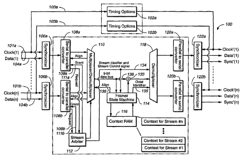
FIG. I is a block diagram of a system according to an implementation of the
invention;
FIG. 2 is a diagram illustrating frame alignment according to an
implementation of the invention;
FIG. 3 is a state machine illustrating frame processing according to an
implementation of the invention.
DETAILED DESCRIPTION OF THE INVENTION
FIGS. 1-3 illustrate an improved frame detection and generation system.
Signal streams are divided into a clock stream and a data stream. Each stream
is
processed independently. A framer unit is provided offset the path of the data
streams to store and update the context of the data streams and to align the
data
stream to the bus.
Turning now to the drawings and, with particular attention to FIG. 1, a block
diagram of a framer array according to an embodiment of the present invention
is
shown therein and identified by the reference numeral 100. Shown are a
plurality of
incoming clock-data pairs 101 a, 101 b for receiving data streams. While only
two
such pairs are shown, in practice, multiple clock-data pairs may be utilized.
The
CA 02434622 2003-07-10
WO 02/060103 PCT/US02/00816
3
clock-data pair may transport data according to the International
Telecommunications Union (ITU) T1 or El Standards.
Each incoming data path includes a clocking branch 103a, 103b and a data
branch 104a, 104b. The clocking branch includes timing options 102a, 102b for
each data path. The timing options 102a, 102b may be any suitable circuitry,
such
as application specific integrated circuits (ASICs), for extracting the clocks
from the
respective paths and may perform various functions on the clock, such as de-
jittering.
Each data branch 104a, 104b includes a synchronizer 106a, 106b for
receiving the incoming data streams. The outputs of the synchronizers 106a,
106b
are serial data streams synchronous to a system clock (not shown) and are
provided
to serial-to-parallel converters 108a, 108b. The outputs of the serial-to-
parallel
converters 108a, 108b are provided to a multiplexer 110.
A stream arbiter 112 controls the output of the multiplexer 110. As
illustrated, each serial-to-parallel converter 108a, 108b is connected via a
request
signal line 109a, 109b to the stream arbiter 112. Thus, once an incoming
stream
has been converted, the serial-to-parallel converter 108a, 108b sends a
request
along the request line 109a, 109b to the stream arbiter 112. The stream
arbiter 112
provides a grant signal 111 a, 111 b to each serial-to-parallel converter
108a, 108b
according to a predetermined selection algorithm. The stream arbiter 112 may
implement any of a variety of known selection algorithms, such as round-robin,
and
the like. The stream arbiter 112 may be implemented as one or more embedded
controllers or processors or ASICs.
The multiplexer 110 outputs a stream identifier 134 and parallel data on the 9
bit wide internal data bus 136. As will be described in greater detail below,
the
multiplexer 110 further receives an align signal 138 from a framer state
machine
114, which is used to align the incoming data to the 9-bit data bus 136.
A framer state machine 114 and context RAM 116 are coupled to the stream
identifier and stream control signal 134 and the 9-bit data bus 136. As will
be
described in greater detail below, the framer state machine 114 operates on
the data
streams by loading and storing the context of individual streams in the
context RAM
116. "Context" is various information related to the data and streams. The
framer
CA 02434622 2006-07-06
29903-137
4
state machine 114 identifies the start of frames of passing
data streams using, for example, any of a variety of known
search algorithms such as identifying a start of frame bit
or bits. The framer state machine 114 further aligns the
incoming data to the 9-bit data bus 136, as will be
described in greater detail below. The framer state machine
114 may also insert alarms, a framing pattern, or similar
information by adding such information via a multiplexer 133
to the 9-bit data bus 136. The framer state machine further
outputs an outset identifier 135 to a demultiplexer 118.
The modified outgoing data stream is demultiplexed
with the demultiplexer 118 onto parallel-to-serial
converters 120a, 120b. The demultiplexer 118 uses the
stream identifier 134 to identify the correct stream for
demultiplexing. The outputs of the demultiplexer 118 are
provided to parallel-to-serial converters 120a, 120b for
conversion back to serial format. The serialized data
streams are then re-synchronized to their original clocks in
the synchronizers 122a, 122b.
During operation, data is placed on the 9-bit data
bus 136 together with a stream identifier and stream control
signals 134. When new data is placed on the internal bus,
the framer state machine 114 loads the context of the stream
to be processed. After processing of the data is finished,
the framer state machine 114 stores the current context of
the stream in its context RAM 116.
The framer state machine 114 calculates the frame
position of the new stream in any of a variety of known
manners. If the framer array 114 finds the frame boundary
of the data stream and the data stream is not aligned, the
framer state machine 114 aligns the time slots of the
CA 02434622 2006-07-06
29903-137
4a
incoming frames to the 9-bit data bus 136. This is
accomplished using the align signal 138, which informs the
serial-to-parallel converter 108a, 108b to provide, for
example, nine bits during the next data transfer. Thus,
time slots of the frame will be aligned in a maximum of
seven data transfers as the time slot can be shifted one bit
per transfer.
This process of frame alignment is illustrated
more clearly with reference to FIG. 2. Shown are Time
Slot 0, Time Slot 1, Time Slot 2, and Time Slot 3 of an
incoming frame.
During normal operation eight data bits are
transported over the 9-bit data bus together with the
respective stream identifier. As shown, the data bits
transported over the 9-bit data bus 136 during the initial
data transfer are misaligned
CA 02434622 2003-07-10
WO 02/060103 PCT/US02/00816
to the incoming frame by one (1) bit. In particular, 210 shows a data transfer
where
bit 256 of a previous frame and bits I through 7 of the actual frame are
transported
over the 9-bit data bus 136. After the next transfer 212 the framer state
machine 114
finds the frame begin. The state machine 114 detects the misalignment as
described above and then requests a nine bit data transfer via the align
signal 214 in
order to align the data to the 9-bit data bus 136. 214 shows the following
nine bit
data transfer which aligns time slot 2 to the internal bus. If the frame and
the time
slot had been misaligned by more than one (1) bit, the process would repeat
until
the frame and time slot were aligned, as shown at 216.
A state diagram of framer state machine handling of the El double frame
format is shown in FIG. 3. After startup, the framer state machine is in an
initial
state 302. When a data stream is enabled for operation, the framer state
machine
114 enters a "Wait for 8" state 304. This state is implemented to fetch the
first byte
from the internal bus. Afterwards, the framer state machine enters a "Search
for
FAS (first frame alignment signal)" state 306. The framer state machine
remains in
this state as long as it hasn't found the frame alignment signal in the El
stream.
When found, the framer state machine 114 steps to the 'Wait until second
frame'
state 308. When the beginning of the second frame is reached, the framer state
machine 114 moves on to the 'Verify Service Word' state 310. Here the framer
state
machine 114 checks the service word. If incorrect, it steps back into the
'Search for
first FAS' state 306. Otherwise it steps to the 'Wait until third Frame' state
312.
When the beginning of the third frame is reached, the framer state machine 114
steps forward to the 'Verify second FAS' state 314 where it checks again for
the
frame alignment signal. If incorrect, the framer state machine 114 goes back
to the
'Search first FAS' state. Otherwise it goes forward to the 'Step Phase' state
316. In
this state, the framer state machine 114 checks if the octet structure of the
El frame
is aligned to the internal data bus. When aligned, the framer state machine
114
moves forward to the 'Aligned' state 318. If the original stream is not
aligned to the
internal data bus, the framer state machine 114 remains in the 'Step Phase'
state
316 until the stream is aligned. To align the stream, the framer requests nine
bits of
data until the octets (or time slots) of a frame are aligned to the 9-bit data
bus.
When aligned, the framer state machine 114 steps into the 'Aligned' state 318.
The
CA 02434622 2003-07-10
WO 02/060103 PCT/US02/00816
6
framer state machine 114 remains in this state until it goes out of
synchronization
(i.e., not aligned any more). In this case, the framer state machine returns
to the
'Search first FAS' state 306, or the 'Init' state 302 when frame processing is
disabled
(framer turned off).
The invention described in the above detailed description is not intended to
be limited to the specific form set forth herein, but is intended to cover
such
alternatives, modifications and equivalents as can reasonably be included
within the
spirit and scope of the appended claims.