Note: Descriptions are shown in the official language in which they were submitted.
CA 02434681 2003-07-09
PIXEL CIRCUITRY FOR IMAGING SYSTEM
BACKGROUND OF THE INVENTI N
1. Field of Invention
[0001] The present invention relates to imaging systems and methods.
2. Description of Related Art
[0002] Currently, imaging systems are used in a wide variety of fields. For
example, imaging systems are used extensively for medical applications in
assisting a
medical professional to determine the best treatment for a patient.
[0003] Recently, there has been success with large-area imaging systems
and processes that are used as medical imaging systenis. These large-area
imaging
system can use a large number of pixels where a frame time can be quite long,
for
example, the frame time can be nearly 1 second. One frame time is the time
required
for all of the pixels in the imaging system to be read out. Further, because
these
large-area imaging systems can combine a plurality of static images, changes
to one
static image that occur faster than an established frame time are averaged
together
which results in the large-area imaging system displaying blurry images. This
problem can be caused by the inability of pixel circuitry used within the
imaging
system to permit a dynamic response time when an object that is moving is
imaged by
the imaging system.
[0004] Thus, there is a need for an imaging system with a pixel circuitry that
permits a dynamic response time capable of properly managing the frame times
associated with a large number of pixels so that the images will not appear as
blurry
images when they are displayed. There is an additional need for the ability to
synchronize the imager response to external events such as a strobe light, x-
ray
source, or an object moving into an appropriate position for imaging.
SUMMARY OF THE INVENTION
[0005] The invention provides imaging systems that use a pixel circuitry to
scan a rapidly changing image.
[0006] The invention further provides imaging systems that include a pixel
circuitry that is used so that images can be taken of a dynamic signal with
time scales
much shorter than the time frame.
CA 02434681 2003-07-09
2
[0007] The invention separately provides imaging systems that include a
pixel circuitry that provides a faster exposure rate, so that any movement
which takes
place during the exposure does not blur the image.
[0008] In various exemplary embodiments of the imaging systems according
to the invention, an imaging system can include at least a two-dimensional
array of
pixels, an input device that includes a sensor that provides an electronic
signal that
represents to the image two-dimensional array of pixels, and a controller, the
electronic signal is controlled by a controller so that the electronic signal
is either
stored in the first capacitor, or stored in the second capacitor.
[0009] In various exemplary altemative embodiments of the imaging
systems according to the invention, the electronic signal can be controlled by
the
controller so that the electronic signal is either stored in the first
capacitor during a
phase of one of the control signals, or not stored in the first capacitor
during a phase
of another one of the control signals.
[0010] In various exemplary alternative embodiments of the imaging
systems according to the invention, an imaging system can include at least a
two-
dimensional array of pixels, an input device that includes a sensor that
provides an
electronic signal that represents to the image two-dimensional array of
pixels, and a
controller that provides a first and second control signal, the electronic
signal being
controlled by the controller so that a charge from the electronic signal is
either added
to the at least one capacitor when a phase of the first control signal is high
and a phase
of the second control signal is low, or the electronic signal is subtracted
from the at
least one capacitor when a phase of the first control signal is low and the
phase of the
second control signal is high.
[0011] In various exemplary alternative embodiments of the imaging
systems according to the invention, two complete pixel. circuitries can both
be
connected to a same sensor. For example, two pixel layouts that include a
capacitor
plus a thin-film transistor can be both connected to the same sensor. During a
determined time frame, the sensor current can be directed to either of the two
capacitors by switching on either a first transistor T, or a second transistor
T2.
Subsequently, both capacitors are read out by activating a gate line for that
specific
capacitor.
CA 02434681 2003-07-09
3
[0012] In various exemplary alternative embodiments of the imaging
systems according to the invention, a switching process within the pixel
circuitry
occurs between two storage capacitors in order to improve the performance of
imaging systems. For example, one capacitor could be independently active for
a
short period of time (greater than 10 microseconds) as compared to the other
capacitor, allowing snapshot imaging of a rapidly cha:riging source.
[0013] Furthermore, a lock-in technique or amplification method can be
applied to enhance data and conditions where image backgrounds are large. In
this
method, a fixed frequency can be used so that the large number of pixels that
are part
of the pixel circuitry are activated at the same frequency. Subsequently, the
difference between stored capacitor values is analyzed so that a rejection of
fixed
signals can be performed.
[0014] In various exemplary alternative embodiments of the imaging
systems and methods according to the invention, a two-color imaging process
can be
performed using the pixel circuitry of the invention by illuminating the
imaging
system with strobe lights of different colors. Then, the image can be stored
in the two
different capacitors so that an object can be imaged in partial color while
the object is
moving.
[0015] In various exemplary alternative embodiments of the imaging
systems according to the invention, a plurality of capacitors can be used with
the pixel
circuitry, for example, three or four capacitors, so that full color can be
achieved with
the imaging system. Moreover, an extra capacitor can be used for storing
leakage
current. Furthermore, a common ground, i.e., short to ground, can used in
conjunction with one capacitor in the pixel circuitry to prevent leakage,
i.e., a part of a
DC component is coupled into other circuits along with an AC component.
[0016] In various exemplary alternative embodiments of the systems and
methods according to the invention, a moving piece of paper can be imaged in
full
color with three strobe lights over a period of less than a hundred
microseconds
allowing the paper to keep moving while imaging systein readout occurs.
[0017] In various exemplary altemative embodiments of the imaging
systems according to the invention, a differential structure can be used as
the pixel
circuitry so that a charge from the sensor is either added to the storage
capacitor
through control signals (1), and 02 when the phase of the control signal cDi
is high and
CA 02434681 2007-09-19
4
the phase of the control signal 4~2 is low, or subtracted from the storage
capacitor
when the phase of the control signal 4~ 1 is low and the phase of the control
signal (D2
is high. Subsequently, a transistor T5 can be switched on while the control
signal 4)I
is high and the control signal (P2 is low in order to read out the storage
capacitor.
[0017A] In accordance with one aspect of the present invention, there is
provided an imaging system, comprising:
an output device including a two-dimensional array of pixels;
an illumination device including two illuminators, each illuminator
capable of illuminating an object with a different color; and
an input device that includes a plurality of pixel devices, each pixel
device including:
a multi-color sensor that provides a first electronic signal representing
the object illuminated by one of the two illuminators and a second electronic
signal
representing the object illuminated by the other of the two illuminators;
at least one transistor connected to the sensor;
a first capacitor that is selectively connected to the sensor;
a second capacitor that is selectively connected to the sensor; and
a controller that selectively stores the entirety of the first electronic
signal in the first capacitor and stores the entirety of the second electronic
signal in
the second capacitor;
wherein each pixel device corresponds to a respective pixel in the two
dimensional array of pixels.
[0017B] In accordance with another aspect of the present invention, there is
provided an imaging system, comprising:
an output device including a two-dimensional array of pixels;
an illumination device including two illuminators, each illuminator
capable of illuminating an object with a different color; and
an input device that includes a plurality of pixel devices, each pixel
device including:
a multi-color sensor that provides a first electronic signal representing
the object illuminated by one of the two illuminators and a second electronic
signal
CA 02434681 2007-09-19
4a
representing the object illuminated by the other of the two illuminators;
at least one transistor connected to the sensor;
a first capacitor that is selectively connected to the sensor;
a second capacitor that is selectively connected to the sensor; and
a controller that: controls the electronic signal that represents a multi-
color image provided by the sensor; and selectively stores the entirety of the
first
electronic signal the first capacitor and stores the entirety of the second
electronic
signal in the second capacitor.
[0018] Additional functions, objects, advantages and features of the present
invention will become apparent from consideration of the following description
and
drawings of exemplary embodiments.
BRIEF DESCRIPTION OF THE DRAWINGS
[0019] These and other features and advantages of this invention are
described in, or are apparent from, the following detailed description of
various
exemplary embodiments of the systems and methods according to this invention,
wherein like numerals reference like elements, and wherein:
[0020] Fig. 1 is an exemplary block diagram of an imaging system;
[0021] Fig. 2 is an exemplary detailed block diagram of a input device used
in the imaging system in Fig. 1;
[0022] Fig. 3 is an exemplary detailed schematic diagram of pixel circuitry
used in the input device in Fig. 2;
[0023] Fig. 4 is a detailed schematic diagram of an exemplary pixel circuitry
that can be used with the systems and methods according to an embodiment of
this
invention;
[0024] Fig. 5 is a detailed schematic diagram of a second exemplary pixel
circuitry for recording only one phase usable with the systems and methods
according
to another embodiment of this invention;
[0025] Fig. 6 is a schematic diagram of a third exemplary pixel circuitry that
can be used with the systems and methods according to another embodiment of
this
invention; and
CA 02434681 2007-09-19
4b
[0025A] Fig. 7 is a schematic diagram of a fourth exemplary pixel circuitry
that can be used with the systems and methods according to another embodiment
of
the invention.
DETAILED DESCRIPTION OF PREFERRED EMBODIMENTS
[0026] In typical imaging systems, pixel circuitry can be used as a layout of
circuits so that the imaging system can control an electrical signal that
represents an
image of an object. For example, the pixel circuitry can be used to accumulate
a
signal from a sensor and allow that signal to be read out in a controlled
manner. In
CA 02434681 2007-09-19
general, the pixel circuitry equates to physical connections that are used by
the
imaging system to control the electric signal from the sensor.
[0027] Fig. 1 shows a block diagram of various components of an imaging
system 1000 that includes various exemplary embodiments according to this
invention. The imaging system 1000 can include components such as an input
device
100, a controller 200, a memory 300, a transmitter 400, an interface device
500 and an
output device 600. The components can be interconnected by a common bus 900.
[0028] The input device can be any device which allows an object to be
input into the imaging system 1000 in order to be imaged. For example, a
scanner can
be used to scan an object to create an electronic image, whereby the resulting
electronic image of the scanned object is input into the imaging system 1000.
Moreover, the input device 100 used with an imaging system 1000 can be a
device
that permits a human body to be scanned as the object, an x-ray imaging
system,
whereby the electronic image of the scanned human body is input into the
imaging
system 1000.
[0029] The controller 200 controls each of the components of the imaging
system 1000 so that an object can be imaged, processed and output through the
output
device 600. The controller 200 can be implemented with a general purpose
processor.
Furthermore, the controller 200 can be implemented using a single special
purpose
integrated circuit, e.g., ASIC, having a main or central processor section for
overall,
system-level control, and separate sections dedicated to performing various
different
specific computations, functions and other processes under control of the
central
processor sections. The controller 200 can be suitably programmed for use with
a
general purpose computer, e.g., a microprocessor, microcontroller or other
processor
device, CPU or NPU, either alone or in conjunction with one or more
peripheral, e.g.,
integrated circuit, data and signal processing devices.
[0030] The memory 300 can be any device capable of storing data or
information for the imaging system 1000.
[0031] The transmitter 400 can be either a single transmitter or a plurality
of
transmitters and any device that transmits, emits or irradiates a signal (or
signals)
towards the object to be imaged so that the input device 100 can form an image
of the
object. For example, the transmitter 400 can be a x-ray source that allows an
x-ray
image to be taken of a human body. Furthermore, the transmitter 400 can be a
light
source that allows an object to be scanned for imaging.
CA 02434681 2007-09-19
6
The interface device 500 allows each component of the imaging system 1000 to
communicate with each other so that the imaging system 1000 can function
normally.
[0032] The output device 600 can be any device capable of receiving the
electronic image of the object and producing an image of the object so the
electronic
image can be viewed. For example, the output device 600 can be a printer that
prints
an image of the scanned object. Furthermore, the output device 600 can be a
display
used to display an electronic image of the scanned object so that an operator
can view
the electronic image. The output device can be any other device that provides
an
image of the object that was input and scanned by the imaging system 1000.
100331 Although these various components of the imaging system 1000 are
discussed for example purposes only, it should be appreciated that the systems
and
methods according to this invention can be used with any components of imaging
systems, and using more or less components, without departing from the spirit
and
scope of the invention. For example, the imaging system 1000 can be an x-ray
imaging system configuration disclosed in U.S. Patent No. 6,408,054 to Rahn et
al.,
for imaging objects that includes an x-ray emitter and an image contrast grid
(antiscatter grid) placed between the x-ray emitter and image contrast grid.
The x-ray
emitter emits x-rays on an object to be imaged, i.e., the human body. The
transmitted
x-rays then strike a surface of a detector within the grid in order to form
the image of
the object.
[0034] Figure 2 shows a more detailed block diagram of an input device 100
that can be used in the imaging system 1000. The input device 100 can include
control electronics 602, receive electronics 604, and many copies of the pixel
circuitry
650. The control electronics 602 can include a plurality of power supplies,
global
control signals to all pixel circuits 650, and sequenced control signals to
individual
pixel circuits. The receive electronics 604 can include a plurality of
amplifiers, analog
filters, analog-to-digital filters, digital filters, and a high-speed data
interface for
sending either analog or digital information to memory 300 or the common bus
900.
[0035] The pixel circuit 650 of the input device can include a sensor such as
an a-Si thin-film photodiode, a lead iodide or mercuric iodide photodetector,
crystalline or polycrystalline silicon, or any other material which provides a
current
dependent on the illumination used in the system. Examples of such materials
are
CA 02434681 2007-09-19
7
described in J. Rahn et al., "High Resolution, High Fill Factor a-Si:H Sensor
Arrays
for Optical Imaging," Materials Research Society Proc. 557, April 1999, San
Francisco, CA; and R.A. Street, "X-ray Imaging Using Lead Iodide as a
Semiconductor Detector," Proc. SPIE 3659, Physics of Medical Imaging, Feb.
1999,
San Diego, CA.
[0036] As previously discussed, the pixel circuitry 650 is the layout of the
circuits which generate signals which represent image information and, under
the
direction of the control electronics 602, send those signals to the receive
electronics
604. A typical imager has millions of pixels. Each pixel has a simple circuit
to detect
the image intensity at that point. The pixel circuitry 650 can be the physical
connections of channels, conductors and equipment which are present at each
pixel in
the imager. The electric signal of the object image is generated by the pixel
circuitry
650. It should be appreciated that for discussion purposes the pixel circuitry
can be
any network or configuration of circuit elements, such as wiring, resistors,
inductors,
capacitors, semiconductors, amplifiers, transistors, inverters, grounds and
any known
or later developed circuitry elements associated with pixels for imaging
systems.
[0037] Figure 3 is a schematic diagram of an exemplary pixel circuitry 650
used in the imaging system 1000 of Figure 1. The pixel circuitry 650 includes
two
transistors T1 and T2, a capacitor 670, a gate line Gl and a control signal (D
1.
Moreover, the pixel circuitry 650 includes a diode 651 and a ground 652.
[0038] Referring to Figure 3, when a signal Vb;as is received from the
control electronics 602, the signal Vb;as is passed through the diode 651 and
input into the source of the transistor T1. The control signal l)1 controls
the signal
or the charge of the signal that is stored in the capacitor 670. When the
control
signal (D controls the signal or charge to be stored in the capacitor 670, the
signal
is sent from the drain of the transistor T1 to the capacitor 670, where the
signal is
stored as a charged signal. Then gate line Gl can be controlled to read out
the
stored signal from the capacitor 670 in order to deliver the signal, to the
receive
electronics via line D1. The gate controls conductance of a channel between
the
source and the drain. An input signal voltage is generally applied to the
gate.
When the gate line Gl is activated, the charged signal stored in the capacitor
670
is sent to the source of the transistor T2 through the gate and then through
the
drain of the transistor T2 to the diode through the data line D1. A copy of
this
circuit exists for each pixel on the imager. For a two-dimensional array, the
line
CA 02434681 2003-07-09
g
Dl is shared among all pixels in the same column, and the gate line G1 is
shared
among all pixels in the same row.
[0039] As previously discussed, a problem associated with the pixel
circuitry 650 shown in Fig. 3 is that the pixel circuitry 650 is unable to
permit a
dynamic response time when an object is moving while being scanned by the
imaging
system 1000. This problem can occur because the single capacitor 670 will
store the
cumulative intensity of the rapidly changing image.
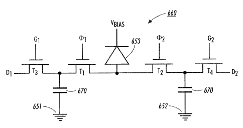
[0040] Accordingly, Fig. 4 is a schematic diagram of an exemplary pixel
circuitry 660 that can be used with the systems and methods according to an
embodiment of this invention to eliminate the above-mentioned problem. In Fig.
4,
the pixel circuitry 660 includes four transistors T] - T4, two capacitors 670-
671, two
gate lines Gi, G2 and two control signals 4)t and 02. Furthermore, the pixel
circuitry
660 includes grounds 651-652 and a photodiode 653.
[0041] It should be appreciated that the transistors T can be semiconductors,
PN junctions, semiconductor diodes or triodes, PNP and NPN transistors, field-
effect
transistors (FET), insulated-gate field-effect transistors (IGFET), junction
field-effect
transistors (JFET), metal-oxide-semiconductor (MOSFET), thin-film transistors
(TFT), or any electronic device used, for example, as an amplifier or switch.
Furthermore, integrated circuits (IC) can be used instead of transistors
within the pixel
circuitry 650.
[0042] The capacitors can be air, silicon oxide, silicon nitride, silicon oxy-
nitride, quartz, polyamide, mica, paper, plastic film, chip, tantalum, disk,
electrolytic
or ceramic type capacitors that function to store an electric charge.
[0043] The amplifiers can be any device that increases the amplitude of the
signal, and can be any class or operation.
[0044] In the pixel circuitry 660 in Fig. 4, when a signal received from the
photodiode 653. Then, the signal is sent to one of the two capacitors 670-671
through
either transistor Tl-T2. The signal, is controlled to be stored in one of the
capacitors
670-671 by the control signals 0r-02 when either control signal 01-02 controls
the
respective transistors Ti-T2 to send the signal to the respective capacitor
670- 671.
The control signals (Dl-02 can be synchronized, for example, with red or green
illumination of the transinitter 400, or any other characteristics of the
transmitter.
Then, gate lines G1-G2 control either transistor T3-T4 to read out the stored
charge of
CA 02434681 2007-09-19
9
each respective capacitor 670-671 in order to send the signal to either diode
line D1-
D2.
[0045] In other words, by configuring the pixel circuitry 660 to connect the
dual pixel circuitries to the same sensor 653, during a determined time frame,
the
signal can be directed to either of the two capacitors 670-671 by switching on
either
the first transistor T1 or the second transistor T2. The dual pixel circuitry
configuration solves the problems that occur when a rapidly moving object is
imaged
in the imaging system 1000 shown in Fig. 1 by adequately being able to store
the
rapidly varying image.
[0046] In various exemplary embodiments according to the invention, either
capacitor 670, 671 can be independently active for a short period of time as
compared
to other capacitor which can allow "snap shot" imaging of a rapidly changing
object.
For example, the capacitor 670 could be independently active for greater than
10
microseconds, with capacitor 671 active for the remainder of the frame time.
[0047] Another application of this configuration relates to the behavior of
certain photodiodes. The depletion depth, or sensitive region, of a photodiode
depends
on the bias voltage applied. Various two-terminal devices have been
demonstrated
which control color sensitivity by adjusting the bias voltage. Examples of
these
devices are disclosed in "Improved Concept for Nipiin and Piiin Color
Sensitive Two-
Terminal Devices with High Linearity," Knipp, D., Stiebig, H., F61sch, J.,
Carius, R.,
and Wagner, H., Mat. Res. Soc. Proc. 467 (1997) 931. Amplifiers in the receive
electronics 604 which reset the capacitors 670-671 to different voltages after
readout
allow the color sensitivity of the photodiode can be controlled at speeds
faster than the
frame time.
[0048] Figure 5 is a schematic diagram of a second exemplary pixel
circuitry 680 usable with the systems and methods according to another
embodiment
of this invention. In the pixel circuitry 680 of Fig. 5, only one capacitor
670 and
grounds 651-652 are used in conjunction with the transistors Tl_T3, photodiode
653
and control signals 4)1-41)2. This configuration can be used as an alternative
pixel
circuitry for recording only one phase of (D 1 or (D2. By adding only a third
transistor
(shown as T2) and by using only the ground 652 and no additional capacitor
(instead.
of four transistors and an two capacitors), the pixel circuitry 680 can
operate as an
image enabler to activate the image in order to eliminate leakage from
occurring
CA 02434681 2007-09-19
through the diode line D1. For example, the configuration of the pixel
circuitry 680
can allow the sensor in the receiver 602 to be blind during one phase of (D 1
and (D 2,
and then activated by reversing the phase. As previous discussed, leakage can
occur in
the convention pixel circuitries. Leakage adds charge to the signal, requiring
corrections to be applied before the image is displayed. Furthermore, leakage
can
also add noise to the image. One application of the image enabler would be to
prevent
leakage current from combining with the signal charge when the image is
expected to
be present only during a small fraction of the frame time.
[0049] When the signal from the photodiode 653 is input into the pixel
circuitry 680, the signal is either controlled by the control signal (D 1 to
be stored in the
capacitor 670 or controlled by control signal 'P2 to be blind using the common
ground
652. When the control signal t1 controls the signal or charge to be stored in
the
capacitor 670, the signal is sent from the drain of the transistor Tl to the
capacitor 670
where the signal is stored as a charged signal. However, when control
signal4)Z
controls the signal from photodiode 653 to be blind, the signal is not sent to
the
capacitor 670, and is instead grounded via the common ground 652. Thus, the
sensor
of the receiver 602 is blind during one phase. Thus, the pixel circuitry 680
configuration according to this embodiment can significantly reduce leakage
that can
occur through the capacitor 670 to the diode line D1 by using the common
ground 652
to blind the receiver 602 at determined phases.
[0050] Referring to Fig. 5, the stored signal in the capacitor 670 is
subsequently read out when the gate line GI is controlled to read out the
stored signal
from the capacitor 670 in order to deliver the signal, for example, to the
diode via line
D1. As with the embodiment in Fig. 4, when the gate line Gl is activated, the
charged
signal stored in the capacitor 670 is sent to the source of the transistor T3
through the
gate and then through the drain of the transistor T3 to the diode through the
readout
line D1 where the signal can displayed to represent the object that has been
imaged.
[0051] Fig. 6 shows a schematic diagram of a third exemplary pixel circuitry
690 that can be used for the systems and methods according to another
embodiment of
this invention. During some imaging, the imaging system 1000 will not require
entire
images in order to provide an output. Instead, the imaging system 1000 only
requires
differences in the entire images to provide an adequate output. With the pixel
circuitry 690 in Fig. 6, the circuitry is used to obtain the differences in
images and
CA 02434681 2007-09-19
11
includes one capacitor 670, a photodiode 651, five transistors T1-T5, a ground
652 and
control signals 4i 142.
[0052] When the signal is received from the photodiode 651, the signal is
then controlled by control signals (D1 or 4?2 so that the charge from the
sensor 653 is
either added to the storage capacitor 670 when control signal4i 1 is high or
control
signa14)2 is low, or subtracted from the capacitor 670 when control signal4? 1
is low
and control signal 4)2 is high. Then the transistor T5 is switched on while
the control
signa14;1 is high and control signal 4?2 is low in order to read out the
storage capacitor
670, and then transistor T5 is switched off while the control signal t 1 is
low and
control signal 4)2 is high. This pixel circuitry 690 can be used where at
least one
difference is required between two images.
[0053] Fig. 7 shows a schematic diagram of a fourth exemplary pixel
circuitry 700 that can be used for the systems and methods according to
another
embodiment of the invention. With the pixel circuitry 700 in Fig. 7, the
circuitry
includes four capacitors 670-673 which are connector to a sensor photodiode
653,
eight transistors T1-T8, grounds 651,654 and control signals 01-04.
[0054] When the signal from the photodiode 653 is input into the pixel
circuitry 700, the signal is controlled by the control signals 01 to be stored
in capacitor
670, 02 to be stored in capacitor 671, 03 to be stored in capacitor 672 or 04
to be stored
in capacitor 673. Control signals 01-04 control respective transistors T1, T2,
T5 and T6.
Then, gate lines Gl-G4 control transistor T3, T4, T7 and T6 respectively to
read out the
stored charge of each respective capacitor 670-673 in order to send the signal
to any
of the diode lines D1-D4.
[0055] While the invention has been described with reference to preferred
embodiments thereof, it is to be understood that the invention is not limited
to the
preferred embodiments or constructions. To the contrary, the invention is
intended to
cover various modifications and equivalent arrangements. In addition, while
the
various elements of the preferred embodiments are shown in various
combinations
and configurations, which are exemplary, at a combination and configuration,
including more or less of a single element, or also within the spirit and
scope of the
invention.