Note: Descriptions are shown in the official language in which they were submitted.
CA 02434955 2005-09-26
ILLUMINATION DEVICE
FOR SIMULATION OF NEON LIGHTING
BACKGROUND OF THE INVENTION
The present invention relates to illumination devices using optical waveguide
and,
more particularly, to lighting devices for the simulation of neon lighting
using optical
to waveguides and high intensity low voltage light sources and ideally adapted
for signage and
advertising uses.
Neon lighting, produced by the electrical stimulation of the electrons in the
low
pressure neon gas filled glass tube, has been a main stay in advertising and
for outlining
15 channel letters and building structures for many years. A characteristic of
neon lighting is
that the tubing encompassing the gas has an even glow over its entire length
irrespective of
the viewing angle. This characteristic makes neon lighting adaptable for many
advertising
applications including script writing and designs because the glass tubing can
be fabricated
into curved and twisted configurations simulating script writing and intricate
designs. The
2o even glow of neon lighting being typically devoid of hot spots allows for
advertising without
visual and unsightly distractions. Thus, any illumination device that is
developed to duplicate
the effects
CA 02434955 2003-07-16
WO 02/061328 PCT/USO1/47629
of neon lighting must also have axially even light distribution over its
length and
substantially even about its circumference. Equally important, such lighting
devices
must have a brightness that is at least comparable to neon lighting. Further,
since
neon lighting is a well established industry, a competitive lighting device
must be
light in weight and have superior "handleability" characteristics in order to
make
inroads into the neon lighting market. Neon lighting is recognized as being
fragile in
nature. Because of the fragility and heavy weight primarily due to its
supporting
infrastructure, neon lighting is expensive to package and ship. Moreover, it
is
extremely awkward to initially handle, install, and/or replace neon lighting
structures.
Any lighting device that can provide those previously enumerated positive
characteristics of neon lighting while minimizing its size, weight, and
handleability
shortcomings will provide for a significant advance in the lighting
technology.
U.S. Patent No 4,891, 896 issued on January 9, 1990 to Boren and assigned to
the Gulf Development Company is an example of many attempts to duplicate neon
lighting. Like this attempt, most prior art neon simulations have resulted in
structures
difficult to fabricate and providing a little in the way of weight and
handling benefits.
The Boren patent exemplifies this by providing a plastic panel with
essentially bas-
relief lettering. The material comprising the lettering is transparent and
coated with a
translucent material. The surrounding material is opaque. When the panel is
back lit
the lettering tends to glow with a neon-like intensity.
The more recent introduction of light weight and breakage resistant point
light
sources as exemplified by high intensity light emitting diodes ("LEDs") have
shown
great promise to those interested in illumination devices that may simulate
neon
2
CA 02434955 2003-07-16
WO 02/061328 PCT/USO1/47629
lighting and have stimulated much effort in that direc'tiori: How"e'vei,"the-
twm
attributes of neon lighting, uniformity and brightness, have proven to be
difficult
obstacles to hurdle as such attempts to simulate neon lighting have largely
been
stymied by the tradeoffs between light distribution to promote the uniformity
and
brightness. For example, U.S. Patent No. 4,976,057 issued December 11, 1990 to
Bianchi describes a device that includes a transparent or translucent hollow
plastic
tubing which is mounted in juxtaposition to a sheet of material having light
transmitting areas that are co-extensive to the tubing . The sheet is back lit
by light
sources such as LEDs which trace the configuration of the tubing. The tubing
can be
made into any shape including lettering. While the tubing may be lit by such
arrangement, the light transfer efficiencies with such an arrangement is
likely to result
in a "glowing" tube having insufficient intensity to match that of neon
lighting. The
use of point light sources such as LEDs may provide intense light that rival
or exceed
neon lighting, but when arranged in arrays lack the uniformity needed and
unfortunately provide alternate high and low intensity regions in the
illuminated
surfaces. Attempts to smooth out the light has resulted in lighting that has
unacceptably low intensity levels.
It is therefore a paramount object of the present invention to provide for an
energy efficient, virtually unbreakable alternative to neon lighting.
A further important object of the present invention is to provide for a
lighting
device that is safe to transport and economical to operate while providing all
of the
application virtues of neon lighting including uniformity and brightness.
3
CA 02434955 2003-07-16
WO 02/061328 PCT/USO1/47629
Yet another object of the present invention is 'to provide
'for'an°'al'feinativ'e to°
neon lighting that is environmentally friendly, requiring no neon gas, and
running on
significantly less electricity that its neon equivalent.
Still another important object is to provide for a neon equivalent that is
easy to
install without complex high voltage electrical installations.
Yet a further object is to provide for a lighting device that can be placed in
hostile environments such as in a freezer case without need for protective
guards
against accidental contact by customers.
These and other objects of the invention will become readily apparent and
addressed through a reading of the discussion below and appended drawings.
1 S SUMMARY OF THE PRESENT INVENTION
The present invention utilizes a profiled rod of material having waveguide
characteristics that preferentially scatters light entering one lateral
surface ("light
receiving surface") so that the resulting light intensity pattern emitted by
another
lateral surface of the rod ("light emitting surface") is elongated along the
length of the
rod. A light source extends along and is positioned adjacent the light
receiving
surface and spaced from the light emitting surface a distance sufficient to
create an
elongated light intensity pattern with a major axis along the length of the
rod and a
minor axis that has a width that covers substantially the entire
circumferential width
of the light emitting surface. In a preferred arrangement, the light source is
a string
4
CA 02434955 2005-09-26
of point light sources spaced a distance apart sufficient to permit the
mapping of the light
emitted by each point light source into the rod so as to create elongated and
overlapping light
intensity patterns along the light emitting surface and circumferentially
about the surface so
that the collective light intensity pattern is perceived as being uniform over
substantially the
entire light emitting surface when being viewed from a normal head-on and side
perspectives.
In one aspect, the invention resides in an illumination device for simulating
neon
lighting, comprising: a substantially rod-like member having a predetermined
length with a
lateral light receiving surface and a lateral curved light emitting surface
having a
to predetermined circumferential width, said member being comprised of a
material that has
both optical waveguide and light scattering properties that preferentially
scatters light entering
said light receiving surface into an elongated light intensity pattern on said
light emitting
surface with a major axis extending along said predetermined length; an
elongated light
source extending along and positioned adjacent said light receiving surface
and spaced from
15 said light emitting surface a sufficient distance to allow said light
intensity pattern on said
emitting surface to have a minor axis extending substantially the entire
circumferential width
of said light emitting surface; a housing in which said light source is
positioned, said housing
extending along said light receiving surface and having a pair of side walls,
each with an
interior light reflecting surface and an exterior light absorbing surface; and
an electric
2o connecting member positioned within said housing and adapted to connect
said light source to
a remote power source.
CA 02434955 2005-09-26
In another aspect, the invention resides in an illumination device for
simulating neon
lighting, comprising: a light transmitting member of a predetermined length
having a
substantially curved front light emitting surface and a light receiving
lateral surface, said
member being comprised of a material that has both optical waveguide and light
scattering
properties that preferentially scatters light entering said light receiving
surface into an
elongated light intensity pattern on said light emitting surface with a major
axis extending
along said predetermined length; a housing having spaced side walls abutting
said light
receiving lateral surface and defining a volume extending along said
predetermined length of
said light transmitting member, said side walls having light reflecting
interior surfaces and
to light absorbing exterior surfaces; and a multiplicity of spaced point light
sources housed
within said volume and extending along said predetermined length, said spaced
point light
sources positioned a distance from said curved front light emitting surface
sufficient to allow
a light intensity pattern from each of said point light sources to overlap
neighboring light
intensity patterns so that the light intensity pattern collectively emitted
from said front light
15 emitting surface appears uniform.
In another aspect, the invention resides in a method of making an illumination
device
capable of simulating neon lighting, comprising the steps of: forming an
essentially solid rod
with a predetermined length and a pair of lateral surfaces from material
having optical
20 waveguide and light scattering properties such that light entering a first
of said lateral surfaces
is caused to form an essentially elliptically shaped light intensity pattern
that has a major axis
in a direction substantially parallel to said predetermined length; placing a
housing having a
pair of spaced walls defining a volume in connected relationship with said
first lateral surface;
5a
CA 02434955 2005-09-26
bending said rod and said housing into a desired shape; positioning a
plurality of spaced point
light sources connected to a flexible electrical connecting member within said
volume
between said side walls; and essentially filling said volume with a potting
material
transmitting light.
In yet another aspect, the invention resides in an illumination device for
simulating
neon lighting, comprising: an essentially solid, leaky waveguide rod having a
predetermined
length with a lateral light receiving surface and a lateral light emitting
surface; an elongated
light source extending substantially along said predetermined length of and
positioned
adjacent to said light receiving surface for emitting a portion of light
emitted by said light
source directly into said light receiving surface; and a housing positioned
externally and
adjacent to said waveguide rod and defining a volume that encompasses said
elongated light
source, whereby said housing includes side walls having internally light
reflecting surfaces
and serves to collect and direct light emitted by said light source into said
lateral light
receiving surface such that light is preferentially directed along the
predetermined length of
the leaky waveguide rod, exiting said light emitting surface in an elongated
light intensity
pattern that has a major axis extending along the length of said waveguide
rod.
DESCRIPTION OF THE DRAWINGS
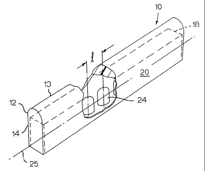
Figure 1 is an elevated perspective view of an illumination device of the
present
invention;
Sb
CA 02434955 2005-09-26
Figure 2 is perspective similar to that of Figure 1 with a portion broken away
to show
the interior;
Figure 3 is an expanded side view of the illumination device as shown in
Figure 1;
Figure 3A is an enlarged wall segment of the illumination device shown in
Figure 3;
Figure 3B is an enlarged wall segment like that shown in Figure 3A with a
variation in
its structure;
Sc
CA 02434955 2003-07-16
WO 02/061328 PCT/USO1/47629
Figures 4, 5, and 6 are respective front, side, and-top elevafiori mews of the
-- ---- ~~~
diodes connected to an electrical board as used in the present invention with
Figure 5
also showing the configuration of the light emitting diodes and electrical
board within
the device;
Figures SA and SB show side views of alternate configurations of the diodes
and electrical board as positioned in the present invention;
Figures 7A and 7B show, respectively, a graph illustrating the light
distribution characteristics of a single point light source and a schematic of
the device
used to measure the same;
Figures 7C and 7D show, respectively, a graph illustrating the light
distribution characteristics of a single point light source mounted within a
device
1 S constructed in accordance with the present invention and a schematic of
the device
used to measure the same;
Figures 7E and 7F show, respectively, a Mercator-like top projection and a
side schematic of the illuminated lateral surface of the waveguide with
overlapping
individual light distribution patterns;
Figure 8 is normalized pattern of the light distribution using an elliptically
shaped LED assisting in creating the elongated light intensity pattern ;
6
CA 02434955 2003-07-16
WO 02/061328 . CT/USO1/47629
Figures 9A, 9B, and 9C show several different' iriterrially'~'o'~ffftsns or me
Lr,~
within the housing of the illumination device in accordance with the present
invention;
Figures l0A and lOB show examples of different housing configurations in
accordance with the present invention;
Figure 11 illustrates the illumination device of the present invention
incorporating a plurality of lines of LEDs;
Figure 12 shows one technique of supporting an illumination device made in
accordance with present invention;
Figure 13 shows a technique of connecting individual lighting devices made in
accordance with the present invention;
Figure 14 shows a variation in the preferred embodiment in which the diodes
are inclined within the housing;
Figure 15 shows still another variation in which the diodes are inverted
within
the housing;
Figure 16 shows an embodiment in which the LED is positioned within a
channel defined in the body of the waveguide itself;
7
CA 02434955 2003-07-16
WO 02/061328 PCT/USO1/47629
Figure 17 illustrates still another embodiment m which the ugnt source is a
light source that itself is elongated and extends in a parallel relationship
to the axis of
the waveguide; and
Figure 18 representing a schematic of electrical circuitry incorporating LEDs
for providing lighting sequences that may be used with the illumination device
of the
present invention.
DETAILED DESCRIPTION OF THE INVENTION
To provide the desired result, i.e., an illumination device that is an
effective
simulator of neon lighting, it is important that the proper materials be
selected for the
component parts and those parts appropriately and geometrically positioned so
that
1 S the resulting illumination device has an essentially uniform light
intensity distribution
pattern over the entire surface with the maximum obtainable brightness. To
accomplish this, it is necessary to use a high intensity but dimensionally
small light
source together with an element that acts both as an optical waveguide and
light
scattering member, but permits light to exit laterally out of its surface (a
"leaky
waveguide"). By placing the light source contiguous such a leaky waveguide in
a
specific manner so as to cause the waveguide to uniformly glow over its
lateral
surface while maximizing the amount of light exiting the surface, applicants
are able
to obtain an illumination device that rivals or surpasses the uniform glow of
neon
tubing. There are many light sources which have the necessary light intensity
output
that is required but most are dimensionally too big to be practical, are
fragile, or
8
CA 02434955 2003-07-16
WO 02/061328 PCT/USO1/47629
consume too much energy. It has been further observed that the best light
source
would likely be one with a small diameter that provided a uniform light output
over
an extended length. However, such light sources have not yet been developed to
the
technological state providing the intensity needed. Thus, applicants have
determined
that the best available light source for the purpose here intended is a string
or strings
of contiguously mounted, essentially point light sources such as spaced apart
high
intensity LEDs.
The ultimate objective of the illumination device of the present invention is
to
simulate an illuminated neon tube that glows with the proper intensity and
uniformity
over its length. Thus, applicants have determined that it is important that
the leaky
waveguide (used to simulate the neon tube) be comprised of a profiled rod of
material
having sufficient diffusivity that collectively with the other components of
the
invention visually eliminates any recognizable individual light distribution
light
pattern that originates from a respective LED or other light source. As stated
above,
the profiled waveguide preferentially scatters light along its length but
ultimately
allows light to exit through its lateral surfaces. Such a waveguide provides a
visible
elongated or oval-like light pattern for each LED, brightest at the center and
diminishing continuously out from the center along the major and minor axis of
the
pattern. By spacing the LEDs a certain distance apart and each LED an
appropriate
distance from the exposed and lateral far side of the leaky waveguide, the
light
intensity distribution patterns on the surface of far side of the leaky
waveguide are
caused to overlap to such an extent that the variations in the patterns are
evened out.
This causes the collective light pattern on the lateral surface to appear to
an observer
to have an uniform intensity along the length of the waveguide. Other
components of
9
CA 02434955 2003-07-16
WO 02/061328 PCT/USO1/47629
the illumination device of the present invention inclutiW g; to~-e~~ri~l'~;
rrie shape ot°
the light sources may assist in establishing the required brightness and
uniformity.
Structurally, the preferred embodiment of the present invention is portrayed
in
Figures 1-6 and shown generally as character numeral 10. The device 10 may be
considered as having two major body components. The first component is a
waveguide 12 having an exposed curved lateral surface 13 serving as the light
emitting surface and a hidden lateral surface 15 (best seen in Figure 3) that
serves as
the light receiving surface. Waveguide 12 is the aforementioned leaky
waveguide
and surface 13 serves as the counterpart to the neon tube. That is, the light
laterally
entering the waveguide from a light source juxtaposed to the surface 15 is
preferentially scattered so as to exit with a broad elongated light intensity
distribution
pattern out of surface 13. Visually, the waveguide 12, when not illuminated
internally, has a milky appearance due to the uniform scattering of ambient
light that
1 S enters the waveguide and that ultimately exits the lateral surface
thereof. Applicants
have found that acrylic material appropriately treated to scatter light and to
have high
impact resistant to be the preferred material for use in forming the waveguide
components of the present invention. When shaped into the profiled rods, the
rods
take on the desired leaky waveguide characteristics. Moreover, such material
is
easily molded or extruded into rods having the desired shape for whatever
illumination application may be desired, is extremely light in weight, and
withstands
rough shipping and handling. While acrylic material having the desired
characteristics is commonly available, it can be obtained, for example, from
AtoHaas,
Philadelphia, Pennsylvania under order number DR66080 with added frosted
characteristics. When shaped into a rod, such acrylic material is observed to
have the
CA 02434955 2003-07-16
WO 02/061328 PCT/USO1/47629
leaky waveguide characteristics desired. Utner matenats sucn as such- as
beactett ww °""' °'
blasted acrylic or polycarbonate, or painted acrylic or polycarbonate provided
with the
desired preferential light scattering characteristics may be used as well for
other
applications.
The second component of the present invention is a housing 14 positioned
adjacent the surface 15 of the waveguide 12. Housing 14 comprises a pair of
side
walls 20, 22 abutting and downwardly extending from the surface 14 and
defining an
open ended channel 18 that extends substantially the length of waveguide 12.
The
housing 14 generally functions to house the light source and electrical
accessories and
to collect light not emitted directly into surface 15 and redirect it to the
waveguide In
other words, the housing further serves to increase the light collection
efficiency by
directing by reflection the light incident upon the internal surfaces of the
housing into
the waveguide 12 and assist in the scattering of the light. From a viewer's
perspective, it is desirable that the visual appearance of the housing 14 not
be
obtrusive with respect to the glowing surface 13 of the waveguide 12; thus, it
is
preferred that the outside surface of the housing be light absorbing and thus
visually
dark to an observer. Again, it is preferred that the housing also be made from
an
impact resistant acrylic material with the outer walls 20 and 22 having an
outer
regions formed from a dark pigmented, thus light absorbing, acrylic while the
inner
regions are made from a white pigmented, thus light reflecting, acrylic. The
two
regions are best viewed in Figure 3A show an enlarged segment of wall 20 in
which
the outer region 20a is the dark acrylic and the inner region 20b is the white
acrylic.
Such acrylic materials preferably are the same as used for the waveguide.
While the
waveguide 12 and housing 14 may be separately formed and then appropriately
11
CA 02434955 2003-07-16
WO 02/061328 PCT/USO1/47629
joined, it is preferred that the components be molded or extruded -as~a umt m
tong
sections with the channel 18 already formed.
An alternate wall structure is shown in Figure 3B in which the wall 20' has
three components, an outer dark region 20c, and intermediate light reflecting
20d, and
a transparent wall 20e which may be comprised of a scattering acrylic like the
waveguide. The outer and intermediate regions 20c and 20d could be dark and
white coatings painted on the wall 20' which itself may be comprised of a
transparent
acrylic material or scattering acrylic. The light reflecting coatings can be
of a color
matching the color of the LED if desired.
Although the above discussion sets forth a preferred construction of the
housing, it should be understood that in some applications the reflecting and
absorption characteristics may be provided by light reflecting and absorption
paint or
tape. Additionally, where there is little concern about the visibility of the
housing, it
may not be necessary to provide the light reflecting and/or absorption
characteristics
to the outer surface of the side walls.
One the most beneficial attributes of the present invention is the ease that
the
illumination device 10 can be bent to form designs or lettering. The channel
18
permits the device 10 can easily be deformed and bent into the desired shape.
Once
the device 10 has been shaped, the LEDs 24 and the electrical connection board
26
are then inserted into the channel 18 and then the channel 18 be filled with a
filler
compound. Thereafter the filler or potting compound is permitted to harden,
thus
maintaining the positioning of the LEDs and circuit board 26. There are
various
12
CA 02434955 2003-07-16
WO 02/061328 PCT/USO1/47629
contigurarions of the LEDs 24 and board lb that may be postrioned wnmn me
cnanneu
18. Examples of the configurations are shown in Figures SA and SB. A preferred
configuration is that shown in Figure 5 because of the compact nature of the
arrangement. In this arrangement, it is important, however, to observe the
orientation
S of the circuit board 26 within channel 18 so that the board 26 extends along
the length
of channel to facilitate bending. The flexibility of the circuit board 26 with
attached
LEDs 24 permit this post design insertion into the channel 18 with the apex of
the
LED 24 essentially abutting the lower surface of the waveguide 12 (as
illustrated in
Figure 3). It is also important that the potting compound 30 used to fill
channel 18
have the desired light transmitting characteristics and be effective in
maintaining the
positioning of both the LEDs and the board. The potting compound further
serves to
eliminate air gaps between the LEDs and the waveguide. It is preferable that
the
potting compound harden into an impact resistant material having an index of
refraction essentially matching that of the housing 24a of the LEDs 24 to
minimize
Fresnel losses at the interface there between. The potting compound further
adds
strength to the structure by filling in the channel 18 and assists in reducing
hot spots
from forming on the lateral surface 13. Such potting compounds may be selected
from commonly available clear varieties such as, for example, that obtainable
from
the Loctite Corporation, Rocky Hill, Connecticut under the brand name Durabond
E-
OOCL. As is also seen in Figure 3, the bottom surface of the device 10 may be
covered with a light reflecting surface 32 which may be , for example, a white
potting
compound or paint and this optionally covered with a light absorbing material
34. In
those instances where the selected LEDs 24 have a certain color the light
reflecting
surface may also be selected to have a matching or substantially the same
color. To
13
CA 02434955 2003-07-16
WO 02/061328 _ PCT/USO1/47629., ."
take advantage of ambient light certain dyes may be added to~ theacrylic
material so
that the device 10 exhibits some readily distinguishable coloring upon
viewing.
The intensity of the point light sources preferably used by the present
invention are typically sufficient to provide the requisite brightness. It
bears
repeating that the quintessentially feature of the present invention, however,
is the
careful spreading or distribution of the individual light patterns of the
point light
sources such that the light patterns are preferentially expanded along the
light emitting
surface and form an oblong or oval-like light intensity pattern. Equally
important is
that the minor axis of the oval-like light intensity pattern extends
substantially the
entire circumferential width of the curved light emitting surface. The
preferential
spreading of each of the light intensity patterns along the waveguide also
permits an
the overlapping of the individual light patterns. This in turn enables the
present
invention to provide an observed uniform collective light pattern along and
over the
entire light emitting surface.
There are various parameters that have an impact on both the brightness and
uniformity of the light intensity pattern emitted by the surface 13 of the
waveguide
12. Among the most important are the scattering characteristics of the
waveguide
material, the spacing "1" between LEDs 24 as shown in Figure 2, the tensing
effect of
the LED housing and internal optics where the light emitting portion of the
LED
resides, the shape and structure of the housing, and the distance "d" (shown
in Figure
3) from the apex of the LED housing 24a to the apex point 12a on the lateral
surface
13. To promote uniformity of the light intensity distribution pattern on the
surface of
the waveguide is that the line of LEDs 24 must be positioned a predetermined
14
CA 02434955 2003-07-16
WO 02/061328 PCT/USO1/47629
distance "d" from apex point 12a of the waveguide. Positioning--the LEDs Z4
too ~-
close to the surface will cause a'hot spot", i.e., a region of higher light
intensity to
locally appear on the surface 12a of the waveguide and spoil the quality of
the
uniform glow. Placing in too far from surface 12a will clearly and undesirably
diminish the overall light intensity emanating from the waveguide 12 and may
also
prevent the minor axis of the oblong or elliptical-like pattern from extending
over the
circumferential width of the light emitting surface. As an example only, it
has been
determined that when the curved surface has a radius of curvature of about
3/16
(about 4.76 mm), the device 10 (shown in Figure3) has a height "h" of about 31
mm
and a width "w" of about 9.5 mm , and the LEDs have a candle power of about
280
mcd and are spaced apart about l2mm, the distance "d" should be about 17.75 to
17.80 mm. It should be understood, however, that while the above describes a
preferred waveguide structure that resembles neon tubing dimensionally, other
and
different shapes of waveguides may be used yet still providing the desired
uniform
glow.
To better understand the principal under which the present invention operates,
reference is now made to Figures 7A-7F as examples of the changes of the light
intensity and spread of the light pattern comparing light intensity and spread
of a
typical diode to that of an illuminating device constructed in accordance with
the
present invention. A single LED or point light source provides a narrow light
intensity pattern 54 as graphically portrayed by Figure 7A. Such a graph can
be
generated by using a photocell type of device 50 portrayed in Figure 7B and
progressively measuring the light intensity at various angles from the center
line 51.
This light pattern 54 should be contrasted to the one in Figure 7C in which
the pattern
CA 02434955 2003-07-16
WO 02/061328 PCT/USO1/47629
56 is considerably broader with a concomitant reduction in the intensity along
the
center line 51. Figure 7C represents the broad pattern emitted by the lateral
surface
13 of the waveguide 12 constructed in accordance with the present invention.
As
stated above, it is important that the distance "d" and the LED spaced apart
distance
"1" be such that the oval-like intensity patterns of the individual LEDs
overlap as
portrayed in the schematic representation of Figure 7E and the projection
depicted in
Figure 7C schematically represents a plurality of LEDs 24 providing an
broadened
overlapping elliptical-like light intensity patterns 31 on the lateral surface
13 of the
waveguide 12. Figure 7E is top view using a Mercator-like projection of the
light
pattern areas 24 on the lateral surface. 13. The minor axis of the light
intensity
patterns 31 are represented by dashed lines 33. As stated above, for any given
dimension of the waveguide and spacing of the point light sources, it is
important that
the distance "d" be appropriately set so distance so that the minor axis of
the light
intensity distribution pattern extends substantially the entire
circumferential width of
the curved lateral light emitting surface 13. For purposes of this disclosure
the light
intensity distribution pattern can be defined as the visible area of the light
pattern
extending out from the center region of the area that is visible discernible
by an
observer.
To further assist in the preferential diffusion and scattering of the light
intensity pattern, applicant has further determined that the use of oval
shaped LEDs
as shown in Figure 6 are helpful. The best effect is obtained when the oval
shaped
LEDs are positioned so that the major axis of the elliptically shaped light
patterns
seen in top elevation view is directed along the long axis of the waveguide
12. The
characteristic light pattern of an oval LED is shown in Figure 8 depicting
graphically
16
CA 02434955 2003-07-16
WO 02/061328 PCT/USO1/47629
normalized light intensity along the mayor and minor axis. As can be seen, the
oval
LED tends to direct light along its major axis illustrated by the curve 36.
The light weight and ruggedness of the illumination device 10 of the present
invention lends itself to ready mounting to almost any surface and by a
variety of
mounting techniques. For example, as illustrated in Figure 12, an extended
length of
the device 10 could be mounted in curtain rod fashion to a wall board 44
through the
use of a bracket hook 40 and fastener 42. Moreover, successive lengths of the
device
can be easily juxtaposed such as, for example, depicted in Figure 13 where
dowels
10 46 of matching refractive indices with the material of the waveguides 12,
12' are
inserted in complimentary openings in the respective ends. Other fastening
techniques may be employed including gluing of the various lengths together at
the
ends thereof. In some instances where the lengths when appropriately
supported, the
ends of the lengths may merely be placed in a juxtaposed touching position.
Thus, as
can easily be understood, illumination devices 10 of an indeterminate length
can
easily be installed and supported.
Figures 9A, 9B, and 9C represent in schematic form but a few of the alternate
constructions in which the LEDs 24 are appropriately spaced from the apex
point of
the waveguide. Figure 9A depicts a light scattering spacer member 48 between
the
waveguide 12 and the LED 24. Such spacer 48 could be fabricated from the same
material as the waveguide 12, e.g., a high impact resistant acrylic material.
Figure
9B represents a construction in which the channel 18 is dimensioned so that
the LED
abuts an inner face of the channel and defines a space 50 between the apex of
the
LED housing and the waveguide 12. Figure 3 shows the use of a transparent
potting
17
CA 02434955 2003-07-16
WO 02/061328 PCT/USO1/47629
compound that tills the space between the L~J~ Z4 and wavegmde l 1. l ne
compound
could easily be introduced into the channel 18 after the LED 24 and circuit
board 26
are placed therein.
Figures 1 OA and l OB illustrate that the configuration of the illumination
device 10 including the waveguide and/or housing could be changed as
determined by
the application to which the illumination device may be applied. Figure l0A
depicts
parallel side walls 20, 22 that merge into sharply diverging side walls 23, 25
of the
waveguide 12 while Figure l OB illustrated as structure in which the walls 20,
22
diverge gradually and blend into the diverging side walls 23, 25 of the
waveguide 12.
Figure 11 depicts further variations to the illumination device 10 where
multiple
strings of LEDs may be used in place of the single one discussed above. The
various
other elements including the reflective and absorption layers are not shown to
maintain clarity.
Although it is preferred that the LEDs 24 be oriented in an upright position
as
depicted in Figure 3 in order to provide the most efficient light intensity
along the
light pattern, other positioning arrangements may be used. One example is
shown in
Figure 14 where the positioning of the LEDs is tilted so that central axis 50'
of the
LEDs is placed at some predetermined angle X to the normal orientation 50 of
the
central LED axis to the longitudinal axis 52. Figure 15 shows the LED 24
positioned with the apex positioned downwardly (vertically positioned or
tilted) with
respect to the axial length of the waveguide. The light collection of the
various
reflective surfaces direct the light from the LED 24 to the waveguide for the
scattering
in the same manner as described above.
18
CA 02434955 2003-07-16
WO 02/061328 PCT/USO1/47629
Figure 16 depicts still another structure where the housing 110 of the LED 120
or point light source is incorporated directly in the body of the waveguide
100 with
reflective and absorption layers not shown to maintain clarity.
Technology is being developed where a light source may be fabricated in
elongated or rope form from, for example, sheets of electro-luminescencing
material
that has sufficient light intensity to be juxtaposed to a leaky waveguide in
place of the
strings of LEDs. Figure 17 illustrates that such a construction of an
illumination
device 140 showing an elongated light source 170 extending in a parallel
relationship
with the longitudinal axis of the waveguide 150 within the housing 160.
The thin and flexible circuit board 26 can be obtained from various sources
such, as, for example, Flexible Circuit Technologies, Saint Paul Minnesota.
The
nature of the electrical connection and the circuitry on the board 26 depend
upon the
illumination sequence desired. While the circuitry is not part of the
invention, it
should be observed that the considerable sequence variety is permitted by the
nature
of the structure of the present invention. That is, the light weight,
resistance to the
rigors of packaging, handling, shipping, and installation, and the minimal
heating
aspects of the illumination device permit essentially endless possibilities
for lighting
and color sequences. The circuit board, may for example, be provided with
various
electrical components that permit flashing or fading of the light sources in
timed
sequences and give the effect of movement. Various light source colors can be
used
and flashed/faded in almost any combination. If the LEDs are interlaced with
different colors, then a striping effect can be obtained. Figure 18
illustrates
19
CA 02434955 2003-07-16
WO 02/061328 ...PCT/USO1/47629
schemarically a circuit which may be used mth the present tnventuon. H
mumpncmy
of LEDs 230 are shown connected in series to a remote power source 232 and to
a
NPN transistor 234 in turned connected to a programmable controller 236. The
LEDs
230 may be of the same color or in color groupings as desired. A second set of
LEDs
240 (and additional sets of LEDs) similarly connected to the power source 232,
NPN
transistor 242, and controller 236 may be separately grouped or alternated
with LEDs
230 as desired. Using the former grouping, the controller 236 could be
programmed
to cause the transistors to go on or off, thus causing the first group and
then
succeeding groups of LEDs to pulse or flash, simulating motion. Should each of
the
groups mounted in a device form a sequence of words, for example, "drink
cola", the
words could be flashed in sequence. If the LEDs of various groups were
alternated in
position, the resulting grouping could form a multi-color striping pattern.
From the discussion above, it may now be appreciated that the illumination
device of the present invention is rugged and resists breakage that normally
would be
expected for neon lighting counterparts in shipping and handling. The
illumination
sources, preferably solid state lighting devices such as LEDs, uses far less
electrical
energy and remains relative cool to the touch. This allows the illumination
device of
the present invention to be used in places where the heat generated by neon
lighting
precludes its use. Moreover, the light weight of the illumination device
facilitates
mounting on support structures that could not support the relative heavy
weight of
. neon lighting, and its required accessories including the high voltage
infrastructure .
Finally, the illumination device is flexible in its use, allowing a tremendous
variety of
lighting techniques very difficult to obtain in neon lighting without
substantial
expense. Other advantages and uses of the present invention will be clearly
obvious
CA 02434955 2003-07-16
WO 02/061328 PCT/USO1/47629
to those skilled in the art upon a reading of the disclosure heiem'and' are
mtenaea io
be covered by the scope of the claims set forth below.
21