Note: Descriptions are shown in the official language in which they were submitted.
CA 02434969 2003-07-15
WO 02/060633 PCT/US02/03006
RESISTOR TRIMMING WITIi SMALL UNIFORM SPOT
FROM SOLID-STATE UV LASER
Related Applications
[0001] This patent application derives priority from U.S. Provisional
Application
No. 601266,172, filed February 1, 2001, and from U.S. Provisional Application
No. 60/301,706, filed June 28, 2001.
Federally Sponsored Research or Deyelopment
[0002] Not applicable
Technical Field
[0003] The present invention relates to laser trimming and, in particular, to
laser trimming
thick or thin film resistors with a uniform spot from a solid-state laser.
Background of the Invention
. [0004] Conventional laser systems are typically employed for processing
targets such as
electrically resistive or conductive films of passive electrical component
structures, such as
film resistors, inductors, or capacitors, in circuits formed on ceramic or
other substrates.
Laser processing to trim the resistance values of film resistors may include
passive,
functional, or activated laser trimming techniques such as described in detail
in U.S. Patent
No. 5,685,995 of Sun et al. .
[0005] The following baclcground is presented herein only by way 'of example
to thiclc film
xesistoxs. ~ZG. 1 is an isorhetxic view of a work piece 10, such as a prior
art thick-film
resistor 10a, forming part of a hybrid integrated circuit device, and FIG. 2
is a cross-
sectional side elevation view depicting thick-film,resistor 10a receiving a
conventional laser
output pulse 12. With reference to FIGS. 1 and 2, a conventional thick-film
resistor 10a
typically comprises a thick film layer I4 of a ruthanate or ruthinium oxide
material
extending between and deposited on portions of the top surfaces of metallic
contacts 16.
Layer 14 and metallic contacts 16 are supported upon a ceramic substrate 18,
such as
1
CA 02434969 2003-07-15
WO 02/060633 PCT/US02/03006
alumina. Modern ruthinium-based thick film pastes have been optimized to be
stable after
Iaser trimming with a 1.047 micron (~,m) Nd:YLF laser or a 1.064- ~,m Nd:YAG
laser. .
[0006] With particular reference to FIG. 1, the resistance value of resistor
10a is largely a
function of the resistivity of the resistor material and its geometry,
including length 22,
width 24, and height 26. Because they are difficult to screen to precise
tolerances, thick-
film resistors are intentionally screened to lower resistance than nomimal
values and
trimmed up to the desired values. Multiple resistors 10a having approximately
the same
resistance values are manufactured in relatively large batches and then
subjected to
trimming operations to remove incremental amounts of the resistor material
until the
resistance is increased to a desired value.
[000'Tj With particular reference to FIG. 2, one or more laser pulses 12
remove
substantially the full height 26 of the resistor material within the spot
dimensions 28 of laser
output pulses 12, and overlapping spot dimensions 28 form a kerf 30. A simple
or complex
pattern can be trimmed through the resistor material of a resistor 10a to fine
tune its
resistance value. Laser pulses 12 are typically applied until resistor 10a
meets a
predetermined resistance value.
[0008] FIG. 3 is an isometric view of a portion of a prior art resistor 10
showing for
convenience two common pattern trim paths 32 and 34 (separated by a broken
line)
between metal contacts 16. "L-cut" path 32 depicts a typical laser-induced
modification.
In an L-cut path 32, a first removal strip 36 of resistor material is removed
in a direction
perpendicular to a line between the contacts to make a coarse adjustment to
the resistance
value. Then an adjoining second removal strip 38, perpendicular to the first
removal strip
36, may be removed to make a finer adjustment to the resistance value. A
"serpentine cut"
path 34 depicts another common type or laser adjustment. In a serpentine cut,
34, resistor
material is removed along removal straps 40 to increase the length of film
path 42.
Removal strips 40 are added until a desired resistance value is reached.
Removal strips 36,
38, and 40 are typically the width of a single kerf 30 and represent the
cumulative
"nibbling" of a train of overlapping laser pulses 12 that remove nearly all of
the resistor
material within the prescribed patterns. Thus, when the trinnming operation is
completed,
the kerfs 30 are "clean" with their bottoms being substantially free of
resistor material such
that the substrate 18 is completely exposed. Unfortunately, the formation of
conventional
clean kerfs 30 necessitates a slight laser impingement of the surface of
substrate 18.
2
CA 02434969 2003-07-15
WO 02/060633 PCT/US02/03006
[0009] As film resistors become smaller, such as in the newer 0402 and 0201
chip
resistors, smaller spot sizes are needed. With the 1.047 ~,m and 1.064 ~,m
laser
wavelengths, obtaining smaller spot sizes while employing conventional optics
and
maintaining the standard working distance (needed to avoid ablation debris
and~to clear the
probes) and adequate depth of field (ceramic, for example, is not flat) is an
ever-increasing
challenge. The desire for even more precise resistance values also drives the
quest for
tighter trim tolerances.
[0010] An article by Albin and Swenson, entitled "Laser Resistance Trimming
from the
Measurement Point of View," IEEE Transactions on Parts, Hybrids, and
Packaging; Vol.
PHP-8, No. 2, June 1972, describes measurement issues and the advantages of
using a
solid-state laser for trimming thin film resistors.
[OOlI] Chapter 7 of an NEC instruction manual describes the challenges
encountered when
using an infrared (IR) Gaussian beam to trim resistors, particularly thick
film resistors.
Heat-affected zones (HAZ), cracks, and drift are some of the problems that are
addressed.
[0012] An article by Swenson et al. , entitled "Reducing Post Trim Drift of
Thin Film
Resistors by Optimizing YAG Laser Output Characteristics," IEEE Transactions
o~z
Components, Hybrids, and Manufacturing Technology; December 1978, describes
using
green (532 nm) solid-state laser Gaussian output for trinuning thin film
resistors to reduce
HAZ and post trim drift.
[0013] U.S. Pat. Nos. 5,569,398, 5,685,995, and 5,808,272 of Sun and Swenson
describe
the use of nonconventional laser wavelengths, such as I.3 ~,m, to trim films
or devices to
avoid damage to the silicon substrate and/or reduce settling time during
functional
trimming.
[0014] International Publication No. VJO 99/40591 of Sun and Swenson,
published August
12, 1999, introduces the concept of resistor trimming with an ultraviolet (UV)
Gaussian
laser output. 'With reference to FIG. 4, they employ the UV Gaussian laser
output to ablate
an area 44 of the surface of film resistors to maintain their surface area and
conserve their
high frequency response characteristics. By intentionally retaining a depth 46
of resistor
film in the trimmed areas 44, they avoid having to clean the kerf bottoms 48
and
substantially eliminate the interaction between the laser output and the
substrate 18, thereby
eliminating any problems that might be caused by such interaction.
Unfortunately, surface
3
CA 02434969 2003-07-15
WO 02/060633 PCT/US02/03006
ablation trirruning is a relatively slow process because the laser parameters
must be
carefully attenuated and controlled to avoid complete removal of the resistor
film.
(0015] Microcracking is another challenge associated with using a solid-state
Gaussian laser
beam for trimming resistors. Microcracks, which often occur in the center of a
kerf 30 on
the substrate, may extend into the resistor film causing potential drift
problems.
Microcracks can also cause a shift associated with the temperature coefficient
of resistance
(TCR). Such microcracking is more pronounced in the newer 0402 and 0201 chip
resistors
that are fabricated on thinner substrates 18, with a typical height or
thickness of about 100
to 200 ~Cm, compared to those of traditional resistors. Microcracking in these
thixmer-
substrate resistors can propagate and even result in catastrophic failure or
physical
brealcage, particularly along the trim lcerf 30, of the resistor during
subsequent handling.
Microcracking can also create "preferred" break lines that are more pronounced
than the
desirable break prescribed break Iines in snapstrates.
(0016] Improved resistor trimming techniques are, therefore, desirable.
Summary of the Invention
(0017] An object of the invention is, therefore, to provide an improved system
and/or.
method for solid-state laser trimming.
(0018] Another object of the invention is to provide spot sizes of less than
20 ~.m to trim
smaller chip resistors, such as 0402 and 0201 chips resistors.
[001] Some of the microcracking may be caused by the high intensity center of
the
Gaussian beam spot in much the same way that a Gaussian beam may be
responsible for
damaging the center of a blind via in a Iaser drilling operation (although the
targets and
substrates are different materials). International Publication No. W~ 00/73013
of Dunsky
et al., published December 7, 2000, describes a method for creating and
employing an
imaged shaped Gaussian beam to provide a uniform laser spot, particularly
useful for via
drilling operations.
(0020] An article by Swenson, Sun, and Dunsky, entitled "Laser Machining in
Electronics
Manufacturing: A ~Iistorical Overview," SI'IE's 45"~ Anfzual Meeting, The
intet-natior2al
Sytnposiuf~a on G?ptical Science and Technology; 3uly 30-August 4, 2000,
describes an
improved surface scanning method using a 40 ~.m uniform spot formed by a lens
described
by Dickey et al. in U.S. Pat. No. 5,864,430.
4
CA 02434969 2003-07-15
WO 02/060633 PCT/US02/03006
[0021] The present invention preferably employs a uniform spot, such as an
imaged shaped
Gaussian spot or a clipped Gaussian spot, that is less than 20 ~,m in diameter
and imparts
uniform energy across the bottom of a kerf 30, thereby minimizing the amount
and severity
of microcracking. Where appropriate, these spots can be generated in an
ablative,
nonthermal, UV laser wavelength to reduce the I~AZ and/or shift in TCR. These
techniques can be employed for both thin and thick film resistor processing.
[0022] Additional objects and advantages of this invention will be apparent
from the
following detailed description of preferred embodiments thereof which proceeds
with
reference to the accompanying drawings.
Brief Description of the Drawings
[0023] FIG. 1 is a fragmentary isometric view of a thick-film resistor.
[0024] FIG. 2 is a cross-sectional side view of a thick-film resistor
receiving laser output
that removes the full thickness of resistor material.
[0025] FIG. 3 is a fragmentary isometric view of a resistor showing two common
prior art
trim paths.
[0026] FIG. 4 is an isometric view of a thick-film resistor with a surface
ablation trim
profile.
[0027] FIG. 5 is a simplified side elevation and partly schematic view of an
embodiment of
a laser system employed for trimming films in accordance with the present
invention.
[002] FIGS. 6A-6C is a sequence of simplified irradiance profiles of a laser
beam as it
changes through various system components of the laser system of FIG. 5.
[002] FIGS. 7A-7D are exemplary substantially uniform square or circular
irradiance
profiles.
[0030] FIG. 8 is a graphical comparison of ideal fluence distributions at the
aperture plane
for.imaged shaped output and clipped Gaussian output at several typical
transmission levels
under exemplary laser processing parameters.
[031] FIG. 9 is a graph of via taper ratio as a function of work surface
location relative to
the nominal image plane.
[0032] FIG. 10 is a graph of via diameter as a function of work surface
location relative to
the nominal image plane.
[0033] FIG. 11 is an electron micxograph of kerf showing microcracks formed in
the
substrate of a resistor trimmed by a Guassian beam.
CA 02434969 2003-07-15
WO 02/060633 PCT/US02/03006
[0034) FIG. 12 is an electron micrograph of a kerf showing the absence of
significant
microcracks formed in the substrate of a resistor trimmed by a uniform spot.
Detailed Description of Preferred Embodiments
[0035) With reference to FIG. 5, a preferred embodiment of a laser system 50
of the
present invention includes Q-switched, diode-pumped (DP), solid-state (SS) UV
laser ~2
that preferably includes a solid-state lasant such as Nd:YAG, Nd:YLF, or
Nd:YVOa.
Laser 52 preferably provides harmonically generated UV laser pulses or output
54 at a
wavelength such as 355 nm (frequency tripled Nd:YAG), 266 nm (frequency
quadrupled
Nd:YAG), or 213 nm (frequency quintupled Nd:YAG) with primarily a TEMoo
spatial
mode profile. Skilled persons will appreciate that other wavelengths and their
harmonics
are available from the other listed lasants. For example, preferred YLF
wavelengths
include 349 nm and 262 nm. Skilled persons will also appreciate that most
lasers 52 do not
emit perfect Gaussian output 54; however, for convenience, Gaussian is used
herein
liberally to describe the irradiance profile of laser output 54. Laser cavity
arrangements,
harmonic generation, and Q-switch operation are all well known to persons
skilled in the
art. Details of exemplary lasers 52 are described in International Publication
No. W~
99/40591 of Sun and Swenson.
[0036 Although other solid-state laser wavelengths, such as green (e.g. 532
nm) or IR
(e.g. I.06 ,um or 1.32 ~cm) , could be employed, a UV laser wavelength is
preferred for
trimming because it has an ablative, relatively nonthermal nature that reduces
post trim
drift. A UV laser wavelength also inherently provides a smaller spot size at
the surface of
workpiece 10 than provided by an IR or green laser wavelength employing the
same depth
of field.
[0637] UV laser pulses 54 may be passed through a variety of well-known optics
including
beam expander and/or upcollimator lens components 56 and 58 that are
positioned along.'
beam path 64. LTV laser pulses 54 are then preferably directed through a
shaping and/or
imaging system 70 to produce uniform pulses or output 72 that is then
preferably directed
by a beam positioning system 74 to target uniform output 72 through a scan
lens 80 (The
scan lens is also commonly referred to as a "second imaging," focusing,
cutting, or
objective lens.) to~ a desired laser target position 82 at the image plane on
a workpiece 10,
such as thick film resistors 10a or thin film resistors. Uniform output 72
preferably
6
CA 02434969 2003-07-15
WO 02/060633 PCT/US02/03006
comprises laser output that has been truncated (clipped), focused and clipped,
shaped, or
shaped and clipped.
[0038] Imaging system 70 preferably employs an aperture mask 98 positioned
between an
optical element 90 and a collection or collimation lens I 12 and at or near
the focus of the
beam waist created by optical element 90. Aperture mask 98 preferably blocks
any
undesirable side lobes in the beam to present a spot profile of a circular or
other shape that
is subsequently imaged onto the work surface. Moreover, varying the size of
the aperture
can control the edge sharpness of the spot profile to produce a smaller,
sharper-edged
intensity profile that should enhance the alignment accuracy. In addition, the
shape of the
aperture can be precisely circular or also be changed to rectangular,
elliptical, or other
noncircular shapes that can be used advantageously for resistor trimming.
[0039] Mask 98 may comprise a material suitable for use at the wavelength of
laser output
54. If laser output 54 is UV, then mask 98 may for example comprise a UV
reflective or
UV absorptive material, but is preferably made from a dielectric material such
as UV grade
fused silica or sapphire coated with a multilayer highly UV reflective coating
other UV
resistant coating. The aperture of maslc 98 may optionally be flared outwardly
at its light
exiting side.
[0040] Optical element 90 may comprise focusing optics or beam shaping
components such
as aspheric optics, refractive binary optics, deflective binary optics, or
diffxaetive optics.
Some or all of these may be employed with or without the aperture mask 98. In
one
preferred embodiment, a beam shaping component comprises a diffractive optic
element
(DOE) that can perform complex beam shaping with high efficiency and accuracy.
The
beam shaping component not only transforms the Gaussian irradiance profile of
FIG. 6A to
the near-uniform irradiance profile of FIG. 6Bb, but it also focuses the
shaped output 94 to
a determinable or specified spot size. Both the shaped irradiance profile 94b
and the
prescribed spot size are designed to occur at a design distance Zo down stream
of optical
element 90. Although a single element DOE is preferred, skilled persons will
appreciate
that the DOE may include multiple separate elements such as the phase plate
and transform
elements disclosed in U.S. Pat. No. 5,864,430 of Dickey et al., which also
discloses
techniques fox designing DOEs for the purpose of beam shaping.
[004.] FIGS. 6A-6C (collectively FIG. 6) show a sequence of simplified
irradiance profiles
92, 96, and 102 of a laser beam as it changes through various system
components of laser
7
CA 02434969 2003-07-15
WO 02/060633 PCT/US02/03006
system 50. FIGS. 6~a-6Bc show simplified irradiance profiles 96a-96c of shaped
output 94
(94a, 94b, and 94c, respectively) as a function of distance Z with respect to
Zo' . Zo' is the
distance where shaped output 94 has its flattest irradiance profile shown in
irradiance
profile 96b. In a preferred embodiment, Zo' is close to or equal to distance
Zo.
[0042] With reference again to FIGS. 5 and 6, a preferred embodiment of shaped
imaging
system 70 includes one or more beam shaping components that convert collimated
pulses 60
that have a raw Gaussian irradiance profile 92 into shaped (and focused)
pulses or output
94b that have a near-uniform "top hat" profile 96b, or particularly a super-
Gaussian
irradiance profile, in proximity to an aperture mask 98 downstream of the beam
shaping
component. FIG. 6Ba shows an exemplary irradiance profile 94a where Z < Zo',
and FIG.
6Bc shows an exemplary irradiance profile 94c where Z > Zo' . In this
embodiment, lens
112 comprises imaging optics useful for inhibiting diffraction rings. Skilled
persons will
appreciate that a single imaging lens component or multiple lens components
could be
employed.
[00431 The shaping and imaging techniques discussed above axe described in
detail in
International Publication No. WO 00/73013 published on December 7, 2000. The
relevant
portions of the disclosure of corresponding U.S. Patent Application No.
09/580,396 of
Dunsky et al., filed lVFay 26, 2000 are herein incorporated by reference.
[0044 FIGS. 7A-7D (collectively FIG. 7) show exemplary substantially uniform
irradiance
profiles produced by a Gaussian beam propagating through a DOE as described in
U.S.
l~at. No. 5,864,430. FIGS. 7A-7C show square irradiance profiles, and FIG. 7D
shows a
cylindrical irradiance profile. The irradiance profile of FIG. 7C is
"inverted," showing
higher intensity at its edges than toward its center. Skilled persons will
appreciate that
beam shaping components 90 can be designed to supply a variety of other
irradiance
profiles that might be useful for specific applications, and these irradiance
profiles typically
change as a function of their distance from Zo' . Skilled persons will
appreciate that a
cylindrical irradiance profile such as shown in FIG. 7D is preferably employed
for circular
apertures 98; cuboidal irradiance profiles would be preferred for square
apertures; and the
properties of other beam shaping components 90 could be tailored to the shapes
of other
apertures. For example, for many straight forward via trimming applications,
an inverted
cuboidal irradiance profile with a square aperture in mask 98 could be
employed.
8
CA 02434969 2003-07-15
WO 02/060633 PCT/US02/03006
[0045] Beam positioning system 74 preferably employs a conventional positioner
used for
laser trimming systems. Such a positioning system 74 typically has one or more
stages that
move workpiece 10. The positioning system 74 can be used for moving laser
spots of
shaped output I I8 in an overlapping manner to form kerfs 30 along trim paths
32 or 34.
Preferred beam positioning systems can be found in ESI's Model 2300, Model
4370, or
soon to be released Model 2370 Laser Trimming Systems conunercially available
from
Electro Scientific Industries, Inc. of Portland, Oregon. Other positioning
systems can be
substituted and are well known to practitioners in the laser art.
[0046] An example of a preferred laser system 50 that contains many of the
above-
described system components employs a UV laser (355 nm or 266 nm) in a Model
5200
laser system or others in its series manufactured by Electro Scientific
Industries, Inc. in
Portland, Oregon. Persons skilled in the art will appreciate, however, that
any other laser
type having a Gaussian beam intensity profile (before imaging or shaping as
disclosed
herein), other wavelengths such as I12, or other beam expansion factors can be
employed.
[004'7] Laser system 50 is capable of producing Iaser system output 114 having
preferred
parameters of typical resistor trimming windows that may include: an
ultraviolet
wavelength, preferably between about 180-400 nm; average power densities
greater than
about 100 mW, and preferably greater than 300 mW; spot size diameters or
spatial major
axes of about 5 ~,m to greater than about 50 ~,m; a repetition rate of greater
than about I
lcHz, preferably greater than about 5 lcHz or even higher than 50 kHz;
temporal pulse
widths that are shorter than about I00 ns, and preferably from about 40-90 ns
or shorter; a
scan speed of about 1-200 mm/sec or faster, preferably about 10-100 mm/sec,
and most
preferably about 10=50 mm/sec; and a bite size of about 0.1-20 ~,m, preferably
0.1-10 ~,m,
and most preferably 0.1-5 ~,m. The preferred parameters of laser system output
114 are
selected in an attempt to circumvent thermal or other undesired damage to
substrates 18.
Skilled persons will appreciate that these output pulse parameters are
interdependent and
are dictated by the performance required.
[0048 Skilled persons will also appreciate that the spot area of laser system
output I I4 is
preferably circular or square, but other simple shapes such as ellipses and
rectangles may
be useful and even complex beam shapes are possible with the proper selection
of optical
elements 90 cooperating with a desirable aperture shape in mask 98. Preferred
spot areas
for laser trimming, more particularly for UV laser trimming, are preferably
smaller than
9
CA 02434969 2003-07-15
WO 02/060633 PCT/US02/03006
about 40 ~.m in diameter, more preferably smaller than about 20 ,um in
diameter, and most
preferably smaller than about 15 ~cm in diameter. Skilled persons will
appreciate that
because the spot size of the UPI laser output is smaller than the spot size of
conventional
laser trimming output and because uniform output 72, permits kerfs 30 to have
straight
uniform walls or edges and thus a smaller IiA~, resistors 10a can be trimmed
to tolerances
that are tighter than the tolerances possible for conventional kerf trimming
techniques.
[004] ~ne difference between the Gaussian output 54 and imaged shaped output
118 is
that pulse 94 uniformly illuminates the aperture of mask 98 at all points
while the Gaussian
output 54 has a higher energy density or "hot spot" at its center that may
increase
microcracking and other undesirable damage to ceramic substrate 18. The imaged
shaped
output 118 consequently facilitates formation of kerfs 30 with a very flat and
uniform
bottom 48 at or into ceramic substrate 18, and this flatness and uniformity
are not possible
with an unmodified Gaussian output 54. Moreover, the imaged shaped output l I8
can also
clean the resistor material from the bottom edges of the kerfs 30 more
completely without
rislcing undesirable damage to the underlying substrate 18 because the uniform
shape of
pulse 94 virtually eliminates the possibility of creating a hot spot at the
bottom center of the
kerf 30, so the amount and severity of microcracks are minimized. The trimming
speed
can also be increased with imaged shaped output 118 over that obtainable with
an
unmodified Gaussian output 54. Imaged shaped output 118 can be applied at
greater laser
power than can Gaussian because "hot spot" damage potential can be eliminated
so the bite
size, repetition rate, and beam movement speed can be favorably adjusted to
trim faster.
[0050 Although a clipped Gaussian spot can alternatively be employed
advantageously
over Gaussian output 54, substantially more energy would have to be sacrificed
to obtain
desirable uniformity than with an image shaped output 118. The imaged shaped
output 118
also provides cleaner bottom edges and faster trimming speed than does clipped
Gaussian
output. FIG. 8 shows a comparison of ideal fluence profiles at the aperture
plane for
shaped output 94b and clipped Gaussian output at several exemplary
transmission levels
under typical laser processing parameters. Fluence levels on the workpiece 10
are equal to
the aperture fluence levels multiplied by the imaging de-magnification factor
squared. In
one example, fluences at the aperture edge were about 1.05 Z/cmz and 0.60
3/cm2 or less
for shaped output 94b and clipped Gaussian output, respectively. Thus,~at
workpiece 10,
the fluences at the edge of the imaged spot (kerf edge) were about 7.4 and 4.3
J/can2 for the
CA 02434969 2003-07-15
WO 02/060633 PCT/US02/03006
imaged shaped output II8 and clipped Gaussian output, respectively. The rate
at which
typical resistor materials can be ablated typically, differs between the
center and edge
fluence levels. As a result, processing of each kerf 30 can be completed in
fewer pulses,
with faster scanning speed, or with larger bite sizes (or smaller pulse
overlaps) with the
imaged shaped output 118, increasing the process throughput.
[0051 An example of a strategy for trimming with imaged shaped output 118 in
accordance with these considerations of present invention is described below.
The fluence
across the entire imaged spot can be maintained, for example, at 90 % of the
value at which
unacceptable ceramic penetration or damage occurs, Faamage. For example,
acceptable
ceramic penetration into thick film resistors is typically less than 10 ~,m,
and preferably less
than 5 ,um. The resistor material is then ablated at conditions which will not
cause damage
such as significant microcracking. In contrast, with the clipped Gaussian beam
at T =
50 % , one could maintain the center of the spot at this fluence, in which
case the edges
would be at only 45 % Of Fdamage. Alternatively, the spot edge could be held
at 90 % of
Faamage, in which case the center would be at 180 % of the damage threshold
fluence,
resulting in substantial damage. lVlaintaining the edges of the imaged spot at
high fluence
enables the resistor material to be cleared from the kerf edges with fewer
laser pulses, since
each pulse removes more material. Thus, the trimming throughput of imaged
shaped
output 1 I8 can be much greater than that of the clipped Gaussian output.
[0052 In addition to being able to clean resistor material from the bottom
edges of the
lcerfs 30 faster as discussed above, the imaged shaped output 118 can also
clean the resistor
material from the bottom edges of the kerfs 30 more completely without risking
damage to
the underlying ceramic substrate 18 because the uniform shape of pulse 94
virtually
eliminates the possibility of creating a hot spot at the bottom center of the
kerf 30
[0053 With respect to kerf quality, the imaged shaped output 118 of the
present invention
also provides for a very precise laser spot geometry and permits better taper
minimizing
performance at higher throughput rates than that available with Gaussian or
clipped
Gaussian output, thus providing crisper edges than available with Gaussian
output 54. The
uniform energy across the bottom of the kerfs 30 and the formation of more
precise edges
provides more predictable trim results, including enhanced repeatability and
positioning
accuracy for smaller target areas.
11
CA 02434969 2003-07-15
WO 02/060633 PCT/US02/03006
[0054 FIG. 9 shows the ratio of kerf bottom width to the kerf top width as a
function work
surface location relative to the nominal image plane, z = 0. With reference to
FIG. 9, the
nominal image plane is the location where the kerfs 30 are most taper free,
with the most
sharply defined top edges. Positive values of z represent planes below the
nominal image
plane, i. e. , with the workpiece 10 placed far ther from the system optics
than distance of
separation where z = 0. The 30 error bar is shown for reference because bottom
width
measurements may be difficult to measure reliably. The largest bottom/top
ratio is .
achieved at the image plane where z = 0. Throughout a ~ 400 ,um range, the
bottom/top
ratio was always greater than 75 % at high throughput.
[0055 FIG. 10 shows kerf width as a function of work surface location relative
to the
nominal image plane, where z= 0. As the workpiece 10 is moved further above
the
nominal image plane, the average kerf top width increases steadily. For
locations below
z = 0, the top width remains fairly constant out to 400 ~Cm below the image
plane. The
3a widths are generally held to within ~ 3 ~.m of the average value, with
exceptions at
z = + 300 ~,m and z = -300 ~Cm. For the bottom width, in contrast, the average
value
decreases steadily from locations above to locations below the nominal image
plane.
Because the width of the kerf bottom is significantly more difficult to
control than the size
of the kerf top, the bottom width is shown for reference only. Statistical
process control .
techniques that could be applied to laser system 50 are, therefore, applicable
to the
characteristics of the kerf tops.
[0056). The data in FIGS. 9 and 10 suggest several approaches to managing
depth of focus
issues fox process robustness. If one wishes to maintain a constant kerf top
width over
varying material thicknesses and machine conditions, it would be advantageous
to set up the
process with the work surface located slightly below the nominal image plane
at, say z =
+200 ~.m. This would produce a zone of ~ 200 ~,m of z variation that could be
accommodated with very little effect on the top diameter. If, on the other
hand, it is more
desirable to maintain a constant kerf bottom/top diameter ratio, it would be
better to set up
the process with workpiece 10 located exactly at the nominal image plane. This
would
ensure that the botton~ltop ratio would decrease by no more than 5 % over a z
range of at
least ~ 200 ~,m. The viability of either of these approaches depends on
whether the other
lcerf characteristics remain within acceptable limits as workpiece 10 moves
away from the
nominal image plane.
12
CA 02434969 2003-07-15
WO 02/060633 PCT/US02/03006
[00~7~ Moreover, beam shaping components 90 can be selected to produce pulses
having
an inverted irradiance profile shown in FICI. 7C that is clipped outside
dashed lines 130 to
facilitate removal of resistor material along the outer edges of kerf 30 and
thereby further
improve taper. The present invention permits a taper ratio of greater than 80
% at a
maximum throughput without undesirable damage to ceramic substrate 18, and
taper ratios
of greater than 95 % (for low aspect ratio kerfs 30) are possible without
undesirable damage
to ceramic substrate 18. Better than 75 % taper ratios are even possible for
the smallest kerf
widths, from about 5-18 ~,m width at the kerf top, of the deepest kerfs 30,
with
conventional optics. Although taper ratio is typically not a critical
consideration in many
trimming operations other than the extent to which it impacts lcerf widths on
small resistors
10a, the high taper ratios achievable with the present invention are further
evidence of kerf
bottom uniformity.
[0058] The trimming techniques disclosed herein can be employed for both thick
and thin
film resistor processing applications as described in any of the references
cited in the
background of the invention, including partial depth trimming. With respect to
thick film
resistors, particularly ruthenium oxide on ceramic including the 0402 and 0201
chip
resistors with a ruthenium layer height or thickness of less than about 200
~,m, the preferred
trimming criterion is to remove all of the ruthenium within the kerfs 30 with
a minimal
amount of penetration into the ceramic substrate 18. These desirable kerfs 30
are clean
such that ceramic material is uniformly exposed and the bottom of the kerfs 30
are "white. "
Such cleaning often entails intentional penetration into the ceramic to a
depth of about
0.1-5 pm and often at least 1 ~Cm. The imaged shaped output 118 can provide
these clean
or white kerfs 30 without creating significant microcracking. UV is
particularly preferred
for processing resistor material over ceramic; however, other wavelengths may
be
employed.
[0059] Although a U~ wavelength can be employed, an IR wavelength,
particularly at
about 1.32 ~.m, may be a preferred wavelength for employing a uniform spot to
trim
materials, such as NiCr, SiCr, or TaN, from silicon substrates, especially for
trimaning
active or electro-optic devices and in applications involving functional
trimming.
[0060 Skilled persons will appreciate that the uniform spot trimming
techniques disclosed
herein may be employed on single resistors, resistor arrays (including those
on snapstrates),
voltage regulators, capacitors, inductors, or any other device requiring a
trimming
13
CA 02434969 2003-07-15
WO 02/060633 PCT/US02/03006
operation. In addition, the uniform spot trimming techniques can be employed
for surface
ablation trimming or other applications where the imaged shaped output 118
does not
penetrate the substrate 18, as well as the applications where substrate
penetration is
desirable.
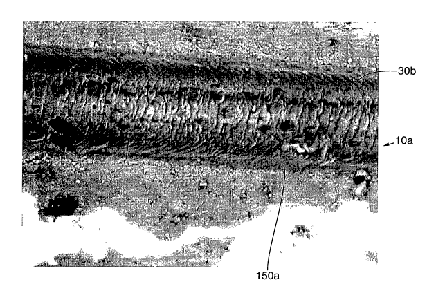
[0061] FIGS. 11 and 12 are electron micrographs showing the differences in
microcracking
between a resistor IOa trimmed with a UV Gaussian beam (FIG. I I) and a
resistor 10a
trimmed with a UV uniform (imaged shaped) beam (FIG. 12). With reference to
FIG. 11,
a reisistor 10a was trimmed with a UV Gaussian output 54 having an average
power of 0.6
W at a repetition rate of 14.29 lcHz at a trim speed of 30 mm/sec with a bite
size of 2.10
~,m. The resulting kerf 30a exhibits numerous microcraclcs substantial
microcraclcs 140, a
substantially wide kerf edge 150a, and deep penetration into the ceramic
substrate 18 at the
center of kerf 30a. With reference to FIG. 12, a resistor 10a was trimmed with
UV imaged
shaped output 118 having an average power of 2.86 W at a repetition rate of 8
kFlz at a
trim speed of 32 mm/sec with a bite size of 4 ,um. The resulting kerf 30b
exhibits no
undesirable damage with few if any microcracks. The kerf edges 150b are
relatively
narrow and the substrate penetration is shallow and substantially uniform.
[0062] It will be obvious to those having skill in the art that many changes
may be made to
the details of the above-described embodiments of this invention without
departing from the
underlying principles thereof. The scope of the present invention should,
therefore, be
determined only by the following claims.
14