Note: Descriptions are shown in the official language in which they were submitted.
CA 02435310 2003-07-18
WO 02/058249 PCT/USO1/49343
1
HIGH EFFICIENCY WIDEBAND LINEAR
WIRELESS POWER AMPLIFIER
Field of the Invention
The present invention relates, in general, to power amplifiers and,
more particularly, to an apparatus, method and system for high efficiency,
wideband
linear power amplification in wireless applications, such as broadband CDMA
and 3G
cellular systems.
Background of the Invention
Power amplifiers for wireless transmission applications, such as radio
frequency ("RF") power amplifiers, are utilized in a wide variety of
communications
and other electronic applications. Ideally, the input-output transfer function
of a
power amplifier should be linear, with a perfect replica of the input signal,
increased
in amplitude, appearing at the output of the power amplifier.
In addition, for greater efficiency, various RF systems, such as cellular
systems, attempt to run power amplifiers at or near their saturation levels,
in which
the actual output power of the amplifier is just below its maximum rated power
output
level. This power output level is generally related to the supply voltage (or
supply
power) to the power amplifier, such that a greater supply voltage will produce
a
correspondingly greater output power from the amplifier; for higher power
input
signals, a correspondingly greater actual power output is required to maintain
the
amplifier at or near saturation. In various prior art amplifiers, however, the
supply
voltage to the power amplifier is fixed. Given a typical usage situation in
which
actual power output from the amplifier may vary by a range of several orders
of
magnitude, use of a fixed supply voltage is highly inefficient, as output
power is often
an order of magnitude below its maximum, and the power amplifier is not
maintained
at or near its saturation levels.
Various techniques have evolved to vary the supply voltage to
maintain the power amplifier at or near saturation. One such technique is
power
supply modulation ("PSM") which varies, or modulates, the supply voltage to
the
power amplifier, in order to maintain the power amplifier at or near
saturation while
CA 02435310 2003-07-18
WO 02/058249 PCT/USO1/49343
2
the input signal varies over time. For PSM, the supply voltage of the
amplifier tracks
the input signal variations, typically utilizing a signal detector in
conjunction with a
tracking power supply. In the prior art, however, the various PSM techniques
have
generally been limited to narrowband applications, or have poor efficiency
characteristics.
For example, one prior art PSM technique, known as Envelope
Elimination Restoration ("EER"), utilizes a limiter to provide an essentially
constant
drive level to the power amplifier to maintain the amplifier in a hard
saturation state
and increase efficiency. Use of the limiter, however, greatly expands the
bandwidth
of the RF signal input to the amplifier, and requires very accurate tracking
of the input
signal envelope, with a power supply switching frequency approximately ten
times
greater than the bandwidth of the RF input signal. As these switching
frequencies
increase, the transistors within the tracking power supply become less
efficient,
resulting in excessive power losses. The resulting bandwidth expansion of the
limiter
also requires the bandwidth capability of the amplifier to be significantly
greater than
the input signal bandwidth, limiting the EER configuration to narrow bandwidth
applications, such as amplitude modulation ("AM") RF broadcasts.
Another prior art PSM technique, known as Envelope Tracking ("ET"),
does not utilize the limiter of EER, and consequently may be suitable for
higher
bandwidth applications. Use of envelope tracking, however, introduces
significant
non-linearities in the output signal of the power amplifier, such as gain
distortions,
phase distortions, and other voltage parasitics. More particularly, while
power
amplifiers comprised of LDMOS (laterally diffused MOSFET) circuitry have good
linearity with respect to input power, such LDMOS and other types of power
amplifiers have large variations in gain and phase as a function of supply
voltage.
When PSM techniques are utilized for amplification efficiency, these non-
linearities
cause intermodulation distortion ("IMD") in multicarrier frequency division
multiple
access ("FDMA") or time division multiple access ("TDMA") systems; and
spectral
growth in code division multiple access ("CDMA") systems. These various
distortions also degrade output signal quality and may have other detrimental
effects,
such as decreased data throughput.
CA 02435310 2003-07-18
WO 02/058249 PCT/USO1/49343
3
As a consequence, a need remains for an apparatus, method and system
to provide high efficiency power amplification in broadband (or wideband)
applications, such as 3G and other wideband cellular or RF applications. Such
an
apparatus, method and system should provide linear power amplification,
minimizing
any phase, gain, and other distortions. In addition, such an apparatus, method
and
system should be cost-effective and capable of implementation in existing RF
transmission systems, such as existing cellular base stations.
Summary of the Invention
An apparatus, method and system are provided for power
amplification of an input signal to produce a substantially linear amplified
output
signal, for broadband wireless applications such as 3G cellular and broadband
CDMA
systems, without creating significant intermodulation distortion or spectral
growth.
The preferred system 100 embodiment includes an envelope detector
1 S 110, a tracking power supply 120, an input signal conditioner 150, and a
power
amplifier 170. The envelope detector 110 is utilized to determine an envelope
detector voltage from the input signal, and the tracking power supply 120 is
utilized to
determine a supply voltage from the envelope detector voltage, preferably as a
substantially quantized version of the envelope detector voltage. The supply
voltage
is utilized to maintain the power amplifier 170 at or near its saturation
level. An input
signal conditioner 150 is utilized to predistort or condition the input
signal, to form a
conditioned input signal, such that when the conditioned input signal is
amplified by
the power amplifier 170 using the supply voltage, the amplified output signal
is a
substantially linear, amplified replica of the input signal.
In response to the supply voltage, the input signal conditioner 150
determines a corresponding phase adjustment and a corresponding gain
adjustment.
In the preferred embodiment, the corresponding phase adjustment is selected
from a
plurality of predetermined phase adjustments in response to the supply
voltage, and
the corresponding gain adjustment is selected from a plurality of
predetermined gain
adjustments, also in response to the supply voltage. The plurality of
predetermined
phase adjustments and the plurality of predetermined gain adjustments are
determined
separately and independently, preferably from respective piecewise linear
mappings
CA 02435310 2003-07-18
WO 02/058249 PCT/USO1/49343
4
of a phase response and a gain response of the power amplifier to a range of
variation
of the supply voltage. The input signal conditioner then modifies the input
signal
using the corresponding phase adjustment and the corresponding gain adjustment
to
produce the conditioned input signal.
S The preferred system 100 embodiment also includes a first delay
circuit 160, to synchronize the input signal with the supply voltage, and a
second
delay circuit 165 to synchronize the supply voltage with the conditioned input
signal.
The apparatus, method and system embodiments of the present
invention provide for high efficiency power amplification in broadband (or
wideband)
applications, such as 3G and other wideband cellular or RF applications,
without
significant bandwidth limitations, without intemodulation distortion, and
without
spectral growth. The various embodiments of the present invention effectively
provide linear power amplification, minimizing any phase, gain, and other
distortions.
In addition, the apparatus, method and system of the present invention are
cost-
effective and capable of implementation in existing RF transmission systems,
such as
existing cellular base stations.
Numerous other advantages and features of the present invention will
become readily apparent from the following detailed description of the
invention and
the embodiments thereof, from the claims and from the accompanying drawings.
Brief Description of the Drawings
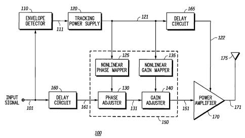
Figure 1 is a block diagram illustrating apparatus and system
embodiments to provide for high efficiency, wideband linear power
amplification in
wireless applications in accordance with the present invention.
Figure 2 is a graphical diagram illustrating an exemplary input signal
voltage, an exemplary envelope detector voltage, and an exemplary tracking
power
supply voltage,, for high efficiency, wideband linear power amplification in
wireless
applications in accordance with the present invention.
Figure 3 is a graphical diagram illustrating an exemplary nonlinear
phase variation, an exemplary piecewise linear mapping to the nonlinear phase
variation, and an exemplary piecewise linear mapping for phase adjustments for
high
CA 02435310 2003-07-18
WO 02/058249 PCT/USO1/49343
efficiency, wideband linear power amplification in wireless applications in
accordance with the present invention.
Figure 4 is a graphical diagram illustrating an exemplary nonlinear
gain adjustment, an exemplary piecewise linear mapping to the nonlinear gain
5 variation, and an exemplary piecewise linear mapping for gain adjustments
for high
efficiency, wideband linear power amplification in wireless applications in
accordance with the present invention.
Figure 5 is a flow diagram illustrating a method embodiment to
provide for high efficiency, wideband linear power amplification in wireless
applications in accordance with the present invention.
Detailed Description of the Invention
While the present invention is susceptible of embodiment in many
different forms, there are shown in the drawings and will be described herein
in detail
specific embodiments thereof, with the understanding that the present
disclosure is to
be considered as an exemplification of the principles of the invention and is
not
intended to limit the invention to the specific embodiments illustrated.
As mentioned above, a need remains for accurate, linear high
efficiency power amplification for broadband or wideband applications. The
apparatus, method and system embodiments of the present invention provide for
such
high efficiency power amplification in broadband (or wideband) applications,
such as
3G and other wideband cellular or RF applications, without significant
bandwidth
limitations, without intemodulation distortion, and without spectral growth.
The
various embodiments of the present invention effectively provide linear power
amplification, minimizing any phase, gain, and other distortions. In addition,
the
apparatus, method and system of the present invention are cost-effective and
capable
of implementation in existing RF transmission systems, such as existing
cellular base
stations.
Figure 1 is a block diagram illustrating apparatus 150 and system 100
embodiments to provide for high efficiency, wideband linear power
amplification in
wireless applications in accordance with the present invention. The system 100
is
CA 02435310 2003-07-18
WO 02/058249 PCT/USO1/49343
6
preferably included within a base station or other transceiver for wireless
communication, such as for 3G cellular systems, wideband CDMA, or other
cellular,
PCS or RF communication systems. The system 100 includes an input signal
conditioner apparatus 150, an envelope detector 110, a tracking power supply
120,
and a power amplifier ("PA") 170. The power amplifier 170 is preferably
coupled to
an antenna (or antenna array) 175 for wireless transmission of an amplified,
output
signal on line 171. As discussed in greater detail below, to provide more
accurate
synchronization of the supply voltage to the power amplifier 170 (on line 122)
with a
conditioned input signal, the system 100 also preferably includes first and
second
delay circuits 160 and 165, respectively.
Continuing to refer to Figure l, the envelope detector 110 and tracking
power supply 120 are utilized to track the input signal (on line 101) and
provide a
variable supply voltage (on line 122) to the power amplifier 170, to maintain
the
power amplifier 170 at or near saturation~and increase the efficiency of the
power
amplifier over a wide range of variation of the input signal. The input signal
conditioner apparatus 150, in accordance with the present invention, includes
a
nonlinear phase mapper 125, a phase adjuster 130, a nonlinear gain mapper 135,
and a
gain adjuster 140. As discussed in greater detail below, the input signal
conditioner
apparatus 150 will essentially predistort (or condition) an input signal (on
line 161)
(which has been delayed (by first delay circuit 160)), to provide a
conditioned input
signal to the power amplifier 170 (on line 151), to counteract any phase and
gain
distortions introduced within the power amplifier 170 from variations in the
supply
voltage (on lines 121 and 122) provided by the tracking power supply 120. As a
consequence, the use of the input signal conditioner apparatus 150, in
conjunction
with the use of the envelope detector 110 and tracking power supply 120 to
vary the
supply voltage to the power amplifier 170, minimizes phase and gain
distortions in the
amplified output signal, and provides for effectively linear, high efficiency
power
amplification in broadband applications.
Figure 2 is a graphical diagram illustrating an exemplary input signal
voltage (205), an exemplary envelope detector voltage (210), and an exemplary
tracking power supply voltage (220), for high efficiency, wideband linear
power
amplification in wireless applications in accordance with the present
invention.
CA 02435310 2003-07-18
WO 02/058249 PCT/USO1/49343
7
Refernng to both Figures 1 and 2, the envelope detector 110 tracks or detects
the
"envelope" of an input signal (on line 101), such as envelope detecting the
exemplary
input signal voltage 205, to produce an envelope detector voltage or signal
(output on
line 111), such as exemplary envelope detector voltage 210. A tracking power
supply
120 is then utilized to further track (or quantize) the envelope detector
voltage (e.g.,
envelope detector voltage 210), and provide a higher or greater level of
supply voltage
and current to the power amplifier 170, in comparison to a level typically
available
directly from an envelope detector 110. In the preferred embodiment, for
faster
operation and for greater bandwidth capability (e.g., to 10 MHz or more), the
tracking
power supply 120 is stepped or switched, providing a quantized power supply
voltage
or signal (on line 121 and, following second delay circuit 165, on line 122)
to power
amplifier 170, such as exemplary power supply voltage 220. As illustrated in
Figure
2, the exemplary power supply voltage 220 output from the tracking power
supply
120 is approximately a stepped or quantized version or replica of the
exemplary
envelope detector voltage 210, and may also include various ringing,
overshoot, and
other voltage distortions, as illustrated by distortions 221 and 222, for
example. By
tracking the input signal (on line 101), the envelope detector 110 and
tracking power
supply 120 provide a variable supply voltage to the power amplifier 170 (on
line 122),
and enable the power arriplifier 170 to be maintained at or near saturation
over a wide
range of magnitudes of the input signal, to provide for highly efficient
amplification
of the input signal.
As mentioned above, however, such envelope tracking by the envelope
detector 110 and tracking power supply 120, to provide a variable supply
voltage to
the power amplifier 170, typically introduces significant non-linearities in
the output
signal (on line 171) of the power amplifier 170, such as gain distortions,
phase
distortions, and other parasitics. More particularly, variations in gain and
phase in the
output signal (on line 171) of the power amplifier 170 are correlated to or
otherwise
occur as a function of the supply voltage (on line 122). These variations in
gain and
phase of the output signal of the power amplifier 170, as a function of supply
voltage,
may be calibrated or otherwise empirically determined, preferably during the
initial
design or manufacture of the power amplifier 170, and may be utilized to
create the
nonlinear phase and gain mappings (illustrated in Figure 3 and 4, for example)
CA 02435310 2003-07-18
WO 02/058249 PCT/USO1/49343
8
respectively implemented in nonlinear phase mapper 12S and nonlinear gain
mapper
135.
Figure 3 is a graphical diagram illustrating an exemplary nonlinear
phase variation (30S), an exemplary piecewise linear mapping to the nonlinear
phase
S variation (dashed lines 310, 31 S and 320), and an exemplary piecewise
linear
mapping for phase adjustments (lines 309, 314 and 319), with respect to supply
voltage, for high efficiency, wideband linear power amplification in wireless
applications in accordance with the present invention. As mentioned above, the
phase
of the amplified output signal from the power amplifier 170 (on line 171), in
comparison to the input signal (on line 101), generally varies as a nonlinear
function
of the supply voltage to the power amplifier (on line 122), and may be
calibrated or
otherwise determined, to provide, for example, exemplary nonlinear phase
variation
305. In the preferred embodiment, a piecewise linear approximation is made to
the
determined nonlinear phase variation, resulting in, for example, an exemplary
1S piecewise linear mapping to the nonlinear phase variation (dashed lines
310, 31S and
320). To predistort the input signal to accommodate this phase variation, a
distortion
opposite to the piecewise linear mapping to the nonlinear phase variation is
utilized,
resulting in an exemplary piecewise linear mapping for phase adjustments
(illustrated
as solid lines 309, 314 and 319 in Figure 3). In the preferred embodiment, a
plurality
of corresponding phase adjustments are stored in the non-linear phase mapper
12S as
a predetermined set of coefficients corresponding to particular supply
voltages. As a
consequence, for any given supply voltage (or range of supply voltages) to the
power
amplifier 170, such as supply voltage level 321, a corresponding phase
adjustment
may be determined by the nonlinear phase mapper 125, such as phase adjustment
322.
2S This phase adjustment, determined by the nonlinear phase mapper 125, will
be
utilized by the phase adjuster 130 (in the input signal conditioner 1 SO) to
predistort or
condition the phase of the input signal, to form an intermediate conditioned
input
signal (on line 131 of Figure 1); this intermediate conditioned input signal
is then gain
conditioned (below), to thereby create a conditioned input signal, (i.e., the
input signal
having been predistorted for both phase and gain variations), which when
amplified
using the supply voltage provided by the tracking power supply 120, will
provide an
CA 02435310 2003-07-18
WO 02/058249 PCT/USO1/49343
9
output signal which is generally or approximately an amplified, linear replica
of the
input signal.
Figure 4 is a graphical diagram illustrating an exemplary nonlinear
gain (or amplitude) variation (325), an exemplary piecewise linear mapping to
the
nonlinear gain variation (dashed lines 330, 335 and 340), and an exemplary
piecewise
linear mapping for gain adjustments (lines 329, 334 and 339), with respect to
supply
voltage, for high efficiency, wideband linear power amplification in wireless
applications in accordance with the present invention. As mentioned above, the
gain
of the amplified output signal from the power amplifier 170 (on line 171), in
comparison to the input signal (on line 101), generally varies as a nonlinear
function
of the supply voltage to the power amplifier (on line 122), and may be
calibrated or
otherwise determined, to provide, for example, exemplary nonlinear gain
variation
325. In the preferred embodiment, a piecewise linear approximation is also
made to
the determined nonlinear gain variation, resulting in, for example, an
exemplary
piecewise linear mapping to the nonlinear gain variation (dashed lines 330,
335 and
340). To predistort the input signal to accommodate this gain variation, a
distortion
opposite to the piecewise linear mapping to the nonlinear gain variation is
utilized,
resulting in an exemplary piecewise linear mapping for gain adjustments
(illustrated
as solid lines 329, 334 and 339 in Figure 4). In the preferred embodiment, a
plurality
of corresponding gain adjustments are stored in the non-linear gain mapper 135
as a
predetermined set of coefficients corresponding to particular supply voltages.
As a
consequence, for any given supply voltage (or range of supply voltages) to the
power
amplifier 170, such as supply voltage level 321, a corresponding gain
adjustment may
be determined by the nonlinear gain mapper 135, such as gain adjustment 323.
This
gain adjustment, determined by the nonlinear gain mapper 135, will be utilized
by the
gain adjuster 140 (in the input signal conditioner 150) to predistort or
condition the
gain of the intermediate conditioned input signal (i.e., the input signal
following its
phase adjustment on line 131 (above)), to thereby create the conditioned input
signal.
The conditioned input signal, which effectively is the input signal having
been
predistorted for both phase and gain variations, when amplified using the
supply
voltage provided by the tracking power supply 120, will provide an output
signal
which is generally or approximately an amplified, linear replica of the input
signal.
CA 02435310 2003-07-18
WO 02/058249 PCT/USO1/49343
It should be noted that the nonlinear phase and gain adjustments, and
their piecewise linear approximations, will generally be different from each
other
(e.g., a nonlinear gain variation, such as exemplary nonlinear gain variation
325, will
have a different calibration (graph or curve), and different piecewise linear
5 approximations, than a nonlinear phase variation, such as exemplary
nonlinear phase
variation 305). As a consequence, in the preferred embodiment, the respective
plurality of nonlinear phase adjustments and plurality of nonlinear gain
adjustments,
as functions of supply voltage, are each calibrated or otherwise determined
separately
and independently. It should also be noted that the phase and gain adjustments
may
10 occur in any order, in addition to that illustrated in Figure 1, such as a
gain adjustment
to create an intermediate conditioned input signal followed by a phase
adjustment, or
a gain adjustment occurnng concurrently with a phase adjustment.
Refernng again to Figure l, for any given input signal at any given
time, the envelope detector 110 tracks or detects the "envelope" of the input
signal (on
line 101), to produce an envelope detector voltage (output on line 111). The
tracking
power supply 120 is then utilized to further track (or quantize) the envelope
detector'
voltage, and provide a higher or greater level of supply voltage and current
to the
power amplifier 170. In the preferred embodiment, the tracking power supply
120 is
stepped or switched, providing a quantized power supply voltage (on line 121
and,
following second delay circuit 165, on line 122) to power amplifier 170. In
the
preferred embodiment, three steps or quantizations are utilized, as any
increased
efficiency available from additional steps would generally be lost from an
increase in
complexity of the tracking power supply 120. To accommodate any delay incurred
during such tracking by the envelope detector 110 and tracking power supply
120,
first delay circuit 160 is utilized to delay and thereby synchronize the input
signal (on
line 161) with a corresponding supply voltage on line 121.
The supply voltage on line 121 is input into both the nonlinear phase
mapper 125 and nonlinear gain mapper 135. As indicated above, for any given
value
of the supply voltage (on line 121), the nonlinear phase mapper 125 and
nonlinear
gain mapper 135 provide a corresponding phase adjustment and a corresponding
gain
adjustment, respectively. Utilizing the corresponding phase adjustment and the
corresponding gain adjustment, respectively, the phase adjuster 130 and the
gain
CA 02435310 2003-07-18
WO 02/058249 PCT/USO1/49343
11
adjuster 140 modify the (delayed) input signal (on line 161), to provide a
predistorted
or conditioned input signal (on line 151) to the power amplifier 170. As
mentioned
above, such gain and phase conditioning may occur in any order, and if
occurring
sequentially, there will be an intermediate conditioned signal, e.g., an
intermediate
phase conditioned input signal followed by the gain conditioning to create the
conditioned input signal, or an intermediate gain conditioned input signal
followed by
the phase conditioning to create the conditioned input signal.
To accommodate any delay incurred during such phase and gain
determinations and adjustments by the input signal conditioner 150, a second
delay
circuit 165 is utilized to delay and thereby synchronize the supply voltage
(on line
122) with the corresponding conditioned input signal (on line 151). The supply
voltage to the power amplifier 170 (on line 122) will then be the same value
as the
supply voltage (on line 121 ) previously provided as inputs to the nonlinear
phase and
gain mappers 125 and 135 and utilized to determine the phase and gain
adjustments to
predistort the input signal to produce the conditioned input signal. As a
consequence,
the amplification of the conditioned input signal by the power amplifier 170,
utilizing
the synchronized supply voltage on line 122, will produce a generally linear,
amplified replica, without phase or gain distortions, of the input signal, on
line 171.
The amplified signal may then be utilized, for example, for broadcast via
antenna 175.
In addition, utilizing the variable supply voltage, determined at any instant
of time by
the corresponding tracking of the input signal, allows the maximum output
power of
the power amplifier 170 to be varied accordingly, thereby allowing the power
amplifier to be maintained at or near saturation over a wide range of input
signal
power levels.
A particularly significant and novel feature of the present invention is
the input of the supply voltage, on line 121, from the tracking power supply
120, into
the input signal conditioner 150, rather than input of the envelope detector
voltage (on
line 111) from the envelope detector 110. As a consequence, the input signal
conditioner 150 may also provide phase and gain adjustments, in the
conditioned
input signal, to additionally accommodate overshoot, ringing and other
nonlinear
distortions, such as distortions 221 and 222 illustrated in Figure 2, which
would
otherwise detrimentally affect the linearity characteristics of the amplified
output
CA 02435310 2003-07-18
WO 02/058249 PCT/USO1/49343
12
signal. In addition, this use of a quantized tracking power supply 120 avoids
the
bandwidth limitations of a continuously tracking power supply, and allows use
of the
system 100 for wideband applications, such as a 10 MHz or greater bandwidth.
Figure 5 is a flow diagram illustrating a method embodiment to
provide for high efficiency, wideband linear power amplification in wireless
applications, and provides a useful summary of the present invention. In the
preferred
embodiment, each step of the method (other than start step 400 and return step
440)
runs or occurs essentially continuously, for as long as an input signal is to
be
amplified, as may be illustrated by the ongoing or continuous operation of the
system
I O I00 circuitry of Figure 1. Referring to Figure 5, the method begins, start
step 400,
with envelope tracking an input signal to produce an envelope detector voltage
(or
signal), step 405, preferably by envelope detector 110. Next, in step 410, the
envelope detector voltage is quantized to produce a supply voltage (or
signal),
preferably by the tracking power supply 120. From the supply voltage, a
corresponding phase adjustment and a corresponding gain adjustment are
determined,
step 415, preferably by the respective nonlinear phase mapper 125 and the
nonlinear
gain mapper 135. As mentioned above, in the preferred embodiment, for an
entire
range of potential supply voltages, a plurality of corresponding phase
adjustments and
a plurality of corresponding gain adjustments are calibrated or otherwise
determined,
and preferably stored as corresponding coefficients in the nonlinear phase
mapper 125
and the nonlinear gain mapper 135, respectively.
Continuing to refer to Figure 5, the input signal is synchronized with
the supply voltage, step 420, preferably by first delay circuit 160. Next, the
synchronized (or delayed) input signal is modified using the corresponding
phase
adjustment and the corresponding gain adjustment, to produce a conditioned
input
signal, step 425, preferably by the phase adjuster 130 and the gain adjuster
140,
respectively. For example, in the preferred embodiment, the phase adjuster 130
and
the gain adjuster 140 may be irr~plemented as multipliers, to multiply the
input signal
respectively by corresponding phase adjustment coefficients and corresponding
gain
adjustment coefficients, to produce the conditioned input signal on line 151.
The
supply voltage, for the power amplifier 170, is synchronized with the
conditioned
input signal, step 430, preferably by the second delay circuit 165. Using the
CA 02435310 2003-07-18
WO 02/058249 PCT/USO1/49343
13
synchronized supply voltage, the conditioned input signal is amplified, such
as by
power amplifier 170, to produce an output signal for transmission on line 171,
step
435. The method may end, return step 440, when there is no longer any input
signal
requiring amplification but, as mentioned above, in the preferred embodiment,
each
step of the method (other than start step 400 and return step 440) runs or
occurs
effectively continuously.
As may be apparent from the discussion above, there are numerous
advantages of the various embodiments of the present invention. The apparatus,
method and system embodiments of the present invention provide for high
efficiency
power amplification in broadband (or wideband) applications, such as 3G and
other
wideband cellular or RF applications, without significant bandwidth
limitations,
without intemodulation distortion, and without spectral growth. The various
embodiments of the present invention effectively provide linear power
amplification,
minimizing any phase, gain, and other distortions. In addition, the apparatus,
method
and system of the present invention are cost-effective and capable of
implementation
in existing RF transmission systems, such as existing cellular base stations.
From the foregoing, it will be observed that numerous variations and
modifications may be effected without departing from the spirit and scope of
the
novel concept of the invention. It is to be understood that no limitation with
respect
to the specific methods and apparatus illustrated herein is intended or should
be
inferred. It is, of course, intended to cover by the appended claims all such
modifications as fall within the scope of the claims.
30