Note: Descriptions are shown in the official language in which they were submitted.
CA 02436146 2003-05-20
WO 02/43302 PCT/USO1/43379
1
METHODS AND APPARATUS FOR SWITCHING ATM, TDM, AND PACKET DATA
THROUGH A SINGLE COMMUNICATIONS SWITCH
BACKGROUND OF THE INVENTION
1. Field of the Invention
The invention relates to telecommunications networks. More particularly, the
invention
relates to methods and apparatus for switching ATM, TDM, and packet data
through a single
communications switch.
2. State of the Art
One of the earliest techniques for employing broadband telecommunications
networks
was called time division multiplexing (TDM). The basic operation of TDM is
simple to
understand. A high frequency signal is divided into multiple time slots within
which multiple
lower frequency signals can be carried from one point to another. The actual
implementation of
TDM is quite complex, however, requiring sophisticated framing techniques and
buffers in
order to accurately multiplex and demultiplex signals. The North American
standard for TDM
(known as T1 or DS1) utilizes twenty-four interleaved channels together having
a rate of 1.544
Mbits/sec. The European standard for TDM is known as E-1 and utilizes thirty
interleaved
channels having a rate of 2.048 Mbits/sec. A hierarchy of multiplexing is
based on multiples of
the T1 or E-I signal, one of the most common being T3 or DS3. A T3 signal has
672 channels,
the equivalent of twenty-eight Tl signals. TDM was originally designed for
voice channels.
Today, however, it is used for both voice and data.
An early approach to broadband data communication was called packet switching.
One
of the differences between packet switching and TDM is that packet switching
includes methods
for error correction and retransmission of packets which become lost or
damaged in transit.
Another difference is that, unlike the channels in TDM, packets are not
necessarily fixed in
length. Further, packets are directed to their destination based on addressing
information
contained within the packet. In contrast, TDM channels are directed to their
destination based
on their location in the fixed frame. Today, a widely used packet switching
protocol is known
as IP (Internet Protocol).
More recently, broadband technologies known as ATM and SONET have been
developed. The ATM network is based on fixed length packets (cells) of 53-
bytes each (48-
bytes payload with 5-bytes overhead). One of the characteristics of the ATM
network is that
CA 02436146 2003-05-20
WO 02/43302 PCT/USO1/43379
2
users contract for a quality of service (QOS) level. Thus, ATM cells are
assigned different
priorities based on QOS. For example, constant bit rate (CBR) service is the
highest priority
service and is substantially equivalent to a provisioned TDM connection.
Variable bit rate
(VBR) service is an intermediate priority service which permits the loss of
cells during periods
of congestion. Unspecified bit rate (UBR) service is the lowest priority and
is used for data
transmission which can tolerate high latency such as e-mail transmissions.
The SONET network is based on a frame of 810-bytes within which a 783-byte
synchronous payload envelope (SPE) floats. The payload envelope floats because
of timing
differences throughout the network. The exact location of the payload is
determined through a
relatively complex system of stuffs/destuffs and pointers. In North America,
the basic SONET
signal is referred to as STS-1 (or OC-1). The SONET network includes a
hierarchy of SONET
signals wherein up to 768 STS-1 signals are multiplexed together providing the
capacity of
21,504 Tl signals (768 T3 signals). STS-1 signals have a frame rate of 51.84
Mbit/sec, with
8,000 frames per second, and 125 microseconds per frame. In Europe, the base
(STM-1) rate is
155.520 Mbidsec, equivalent to the North American STS-3 rate
(3*51.84=155.520), and the
payload portion is referred to as the virtual container (VC). To facilitate
the transport of lower-
rate digital signals, the SONET standard uses sub-STS payload mappings,
referred to as Virtual
Tributary (VT) structures. (The ITU calls these Tributary Units or TUs.) Four
virtual tributary
sizes are defined: VT-1.5, VT-2, VT-3 and VT-6. VT-1.5 has a data transmission
rate of 1.728
Mbids and accommodates a T1 signal with overhead. VT-2 has a data transmission
rate of
2.304 Mbit/s and accommodates an E1 signal with overhead. VT-3 has a data
transmission rate
of 3.456 Mbids and accommodates a T2 signal with overhead. VT-6 has a data
transmission
rate of 6.912 Mbids and accommodates a DS2 signal with overhead.
Each of the above described broadband technologies can be categorized as TDM,
ATM,
or Packet technologies, with SONET being a complex form of TDM. From the
foregoing, it
will be appreciated that TDM, ATM and Packet each have their own unique
transmission
requirements. Consequently, different kinds of switches are used to route
these different kinds
of signals. In particular, TDM requires careful time synchronization; ATM
requires careful
attention to the priority of cells and QOS; and packet (e.g. IP) requires the
ability to deal with
variable length packets. For these reasons, switching technologies for TDM,
ATM, and variable
length packet switching have evolved in different ways. Service providers and
network
designers have thus been forced to deal with these technologies separately,
often providing
overlapping networks with different sets of equipment which can only be used
within a single
network.
CA 02436146 2003-05-20
WO 02/43302 PCT/USO1/43379
SUMMARY OF THE INVENTION
It is therefore an object of the invention to provide methods and apparatus
whereby
different kinds of broadband signals can be switched through a single
switching fabric.
It is also an object of the invention to provide a network element which can
switch TDM,
ATM, and variable length packet traffic all through the same switch fabric.
It is another object of the invention to provide a network switch chipset
which can be
combined with identical chip sets to provide a scalable network switch fabric.
It is a further object of the invention to provide a network switch which
allows flexible
partitioning among TDM, ATM, and variable length packet traffic.
Another object of the invention is to provide a network switch with redundant
switch
planes so that the failure of switch elements or links does not immediately
cause a connection
failure.
A further object of the invention is to provide a network switch which handles
multicast
as well as unicast voice and data transmission.
An additional object of the invention to provide a network switch which
supports Clos
architectures as well as folded Clos architectures.
In accord with these objects which will be discussed in detail below, the
network switch
of the present invention includes at least one port processor (also referred
to in the appendices
as a "service processor") and at least one switch element. The port processor
has a SONET
OC-x (SONET/SDH STS-x/STM-y) interface (for TDM traffic), a UTOPIA and UTOPIA-
frame based interface (for ATM and packet traffic), and an interface to the
switch element. An
exemplary port processor has a total I/O bandwidth equivalent to a SONET OC-48
signal. An
exemplary switch element has 12x12 ports and supports a total bandwidth of 30
Gbps.
A typical switch according to the invention includes multiple port processors
and
multiple switch elements. For a 48x48 "folded" switch, 48 port processors are
coupled (four
each) to 12 (first and third stage) switch elements and each of these twelve
switch elements is
CA 02436146 2003-05-20
WO 02/43302 PCT/USO1/43379
4
coupled to 8 (second stage) switch elements. A three stage non-blocking switch
according to
the invention provides a total bandwidth of 240 Gbps and a five stage non-
blocking switch
provides a total bandwidth of 1 Tbps. An exemplary three stage folded Clos
architecture switch
includes forty-eight port processors and twenty switch elements. Four port
processors are
coupled to each of twelve (first and third stage) switch elements. Each of the
twelve (first and
third stage) switch elements are coupled to eight (second stage) switch
elements. According to
the presently preferred embodiment, each port processor is provided with means
for coupling to
two ports of a switch element or one port of two switch elements thereby
providing redundancy
in the event of a link failure.
According to the invention, a data frame of 9 rows by 1700 slots is used to
transport
ATM, TDM, and Packet data from a port processor through one or more switch
elements to the
same or another port processor. Each frame is transmitted in 125 microseconds,
each row in
13.89 microseconds. Each slot includes a four-bit tag plus a four-byte payload
(i.e., thirty-six
bits). The slot bandwidth (1/1700 of the total frame) is 2.592 Mbps which is
large enough to
carry an E-1 signal with overhead. The four-bit tag is a cross connect pointer
which is set up
when a TDM connection is provisioned. The last twenty slots of the frame are
reserved for link
overhead. Thus, the frame is capable of carrying the equivalent of 1,680 E-1
TDM signals even
though an STM-16 frame has a capacity of only 1008 E-1 signals..
For ATM and packet data, a PDU (protocol data unit) of sixteen slots is
defined for a
sixty-four-byte payload (large enough to accommodate an ATM cell with switch
overhead). A
maximum of ninety-six PDUs per row is permitted. The sixteen four-bit tags of
a PDU are not
needed for PDU routing so they are used as parity bits to protect the ATM or
variable length
packet payload. Of the sixty-four-byte payload, twelve bytes (96 bits) are
used by the switch
for internal routing. This leaves fifty-two bytes for actual payload which is
sufficient to carry an
ATM cell (without the one-byte HEC) and sufficient for larger packets after
fragmentation. The
PDUs are self routed through the switch with a twenty-eight-bit routing tag
which allows
routing through seven switch stages using four-bits per stage. The remaining
sixty-eight bits of
the PDU are used for various other addressing information such as indicating
whether the PDU
contains an ATM cell, a packet, or a control message, whether reassembly of
the packet should
be aborted, whether the payload is a first fragment, middle fragment or last
fragment, how many
payload bytes are in the last fragment, the fragment sequence count, and a
destination flow
identifier.
CA 02436146 2003-05-20
WO 02/43302 PCT/USO1/43379
The link overhead (LOH) in the last twenty slots of the frame is analogous in
function to
the line and section overhead in a SONET frame. The LOH may contain a 36-bit
frame
alignment pattern which is used to delineate the byte and row boundaries from
serial data
streams, a 32-bit status register for each output link, a 32-bit switch and
link identifier, and a 32-
bit stuff pattern.
Since ATM and Packet traffic are typically not provisioned, bandwidth must be
arbitrated among ATM and Packet connections as traffic enters the system.
Moreover, since
TDM traffic shares the same frame as ATM and Packet traffic, bandwidth must be
arbitrated
while maintaining TDM timing. According to the invention, bandwidth is
arbitrated by a system
of requests and grants which is implemented for each PDU in each row of the
frame. The
switch elements provide three channels per link, two of which are used to
carry data and
arbitration requests and one of which is used to carry arbitration grants.
According to the
presently preferred embodiment, a forty-eight-bit ( 1.5 slot) request element
is generated for each
PDU in the next row of the frame. Each switch element includes a single
request parser and a
separate request arbitration module for each output link. The request elements
are generated by
the port processors and include infra-switch "hop-by-hop" routing tags and
priority level
information. Request elements are buffered by the switch elements and low
priority request
elements are discarded by a switch element if the buffer fills. Each request
element which is not
discarded as it travels through the switch fabric is returned to the port
processor from which it
originated during one "row time", i.e. 13.89 microseconds. As suggested above,
requests are
made "in band" interleaved with data and grants (the returned request
elements) are made "out
of band" using the third channel in each link.
In order to maintain timing for TDM traffic, the V 1-V4 bytes in the VT/VC
frame are
stripped off and the VC bytes are buffered at ingress to the switch by a port
processor. The V 1-
V4 bytes are regenerated at the egress from the switch by a port processor. In
rows having both
PDU and TDM traffic, the PDUs are configured early and the TDM slots are
configured late in
the row.
According to the presently preferred embodiments, each switch element includes
a
multicast controller and a separate multicast PDU buffer. Two alternate
embodiments are
provided for multicasting. The first embodiment requires fewer gates and is
best suited for an
environment where multicasting is not a major portion of the traffic. The
second embodiment
requires many more gates to implement. However, it is better suited in an
environment where
multicasting is a frequent event. The second embodiment requires more latency
in setting up a
multicast path, but less latency in multicasting data. According to the first
embodiment,
CA 02436146 2003-05-20
WO 02/43302 PCT/USO1/43379
multicast request elements flow through the switch in the same manner as
standard unicast
request elements. At the point where the message needs to be multicast, the
hop-by-hop field's
bit code for that switch stage indicates that the request is multicast. The
request is forwarded to
the multicast controller. On the grant path, the multicast controller sources
a grant if there is
room for the data in the multicast recirculating buffers. Once the data has
been transmitted to
the multicast buffer, the multicast controller examines the data header and
determines on which
output links it needs to be sent out. At this point, the multicast controller
sources a number of
request messages which are handled in the same manner as unicast requests. The
process
repeats with the sequence of send request, receive grant, transmit PDU. Le,
before each
multicast PDU is transmitted, a request and a grant must traverse the switch.
According to the
second embodiment, a multicast path is reserved for a period of time by
sending multiple
requests (one for each hop) until all hops have been granted. Once the path is
set up in this
manner, PDUs are multicast one after the other with no latency until the
reserved time expires or
there are no more PDUs to transmit.
Additional objects and advantages of the invention will become apparent to
those skilled
in the art upon reference to the detailed description taken in conjunction
with the provided
figures.
BRIEF DESCRIPTION OF THE DRAWINGS
Figure I is a simplified schematic diagram of a port processor according to
the
invention;
Figure 2 is a simplified schematic diagram of a switch element according to
the
invention;
Figure 3 is a schematic diagram illustrating the data frame structure of the
invention;
Figure 3a is a schematic diagram illustrating the presently preferred format
of a PDU
according to the invention;
Figure 3b is a schematic diagram illustrating the row structure including
request
elements to a first stage of the switch;
CA 02436146 2003-05-20
WO 02/43302 PCT/USO1/43379
7
Figure 3c is a schematic diagram illustrating the row structure including
request
elements to a second stage of the switch;
Figure 4 is a schematic illustration of a three stage 48x48 switch according
to the
invention; and
Figure 5 is a schematic illustration of a 48x48 folded Clos architecture
switch according
to the invention.
DETAILED DESCRIPTION OF THE PREFERRED EMBODIMENTS
The apparatus of the invention generally includes a port processor and a
switch element.
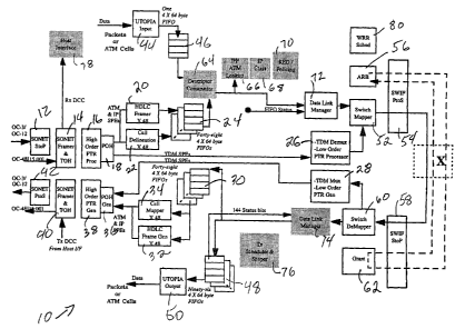
Figure 1 illustrates the main features of the port processor 10, and Figure 2
illustrates the main
features of the switch element 100. Refernng now to Figure 1, the port
processor 10 includes a
SONET interface and a UTOPIA interface. On the ingress (RX) side, the SONET
interface
includes a serial to parallel converter 12, a SONET framer and transport
overhead (TOH)
extractor 14, a high order pointer processor 16, and a path overhead (POH)
extractor 18. For
ATM and IP packets transported in an SPE, the ingress side of the SONET
interface includes
forty-eight HDLC framers 20 (for IP), forty-eight cell delineators 22 (for
ATM), and forty-eight
64-byte FIFOs 24 (for both ATM and IP. For TDM signals transported in an SPE,
the ingress
side of the SONET interface includes a demultiplexer and low order pointer
processor 26. On
the egress (TX) side, the SONET interface includes, for TDM signals, a
multiplexer and low
order pointer generator 28. For ATM and IP packets transported in an SPE, the
egress side of
the SONET interface includes forty-eight 64-byte FIFOs 30, forty-eight HDLC
frame
generators 32, and forty-eight cell mappers 34. The egress side of the SONET
interface also
includes a POH generator 36, a high order pointer generator 38, a SONET framer
and TOH
generator 40, and a parallel to serial interface 42. On the ingress side, the
UTOPIA interface
includes a UTOPIA input 44 for ATM and Packets and one 4x64-byte FIFO 46. On
the egress
side, the UTOPIA interface includes ninety-six 4x64-byte FIFOs 48 and a UTOPIA
output 50.
The ingress portion of the port processor 10 also includes a switch mapper 52,
a parallel
to serial switch fabric interface 54, and a request arbitrator 56. The egress
portion of the port
processor also includes a serial to parallel switch fabric interface 58, a
switch demapper 60, and
a grant generator 62.
CA 02436146 2003-05-20
WO 02/43302 PCT/USO1/43379
8
For processing ATM and packet traffic, the port processor 10 utilizes, at the
ingress
portion, a descriptor constructor 64, an IPF and ATM lookup processor 66, an
IP classification
processor 68, an RED/Policing processor 70, all of which may be located off
chip. These units
process ATM cells and packets before handing them to a (receive) data link
manager 72. At the
egress portion of the port processor, a (transmit) data link manager 74 and a
transmit scheduler
and shaper 76 are provided. Both of these units may be located off chip. The
port processor is
also provided with a host interface 78 and a weighted round robin scheduler
80.
The purpose of the port processor at ingress to the switch is to unpack TDM,
Packet,
and ATM data and frame it according to the data frame described below with
respect to Figure
3. The port processor also buffers TDM and packet data while making
arbitration requests for
link bandwidth through the switch element and grants arbitration requests
received through the
switch as described in more detail below. In order to maintain timing for TDM
traffic, the V 1-
V4 bytes in the SONET frame are stripped off and the VC bytes are buffered at
the ingress to
the switch. In rows having both PDU and TDM traffic, it is preferable that the
PDUs are
configured early and the TDM slots are configured late in the row. At the
egress of the switch,
the port processor reassembles TDM, Packet, and ATM data. The V 1-V4 bytes are
regenerated
at the egress from the switch.
Though not shown in Figure 1, the port processor 10 includes dual switch
element
interfaces which permit it to be coupled to two switch elements or to two
ports of one switch
element. When both interfaces are used, the "standby" link carnes only frame
information until
a failure in the main link occurs and then data is sent via the standby link.
This provides for
redundancy in the switch so that connections are maintained even if a portion
of the switch fails.
Turning now to Figure 2, a switch element 100 according to the invention
includes
twelve "datapath and link bandwidth arbitration modules" 102 (shown only once
in Figure 2 for
clarity). Each module 102 provides one link input 104 and one link output 106
through the
switch element 100. Those skilled in the art will appreciate that data
entering any link input can,
depending on routing information, exit through any link output. According to
the invention,
each module 102 provides two forward datapaths 108, 110, 112, 114 and one
return "grant" path
116, 118. The three paths are collectively referred to as constituting a
single channel. The
reason why two datapaths are provided is to increase the bandwidth of each
channel. The two
datapaths are interleaved to provide a single "logical" serial datastream
which exceeds (doubles)
the bandwidth of a single physical datastream. Data is routed from an input
link 104 to an
CA 02436146 2003-05-20
WO 02/43302 PCT/USO1/43379
9
output link 106 via an input link bus 120 and an output link bus 122. Return
path grants are
routed from an output link 106 to an input link 104 via a grant bus 124.
The forward datapaths of each "datapath and link bandwidth arbitration module"
102
include a data stream deserializer 126, a data stream demapper 128, a row
buffer mapper 130, a
row buffer 132, a request arbitration module 134, a data stream mapper 136,
and a data stream
serializer 138. The return grant path for each module 102 includes a grant
stream deserializer
140, a grant stream demapper 142, a grant arbitration module 144, a grant
stream mapper 146,
and a grant stream serializer 148.
The switch element 100 also includes the following modules which are
instantiated only
once and which support the functions of the twelve "datapath and link
bandwidth arbitration
modules" 102: a link synchronization and timing control 150, a request parser
152, a grant
parser 154, and a link RISC processor 156. The switch element 100 also
includes the following
modules which are instantiated only once and which support the other modules,
but which are
not directly involved in "switching": a configuration RISC processor 158, a
system control
module 160, a test pattern generator and analyzer 162, a test interface bus
multiplexer 164, a
unilink PLL 166, a core PLL 168, and a TTAG interface 170.
A typical switch according to the invention includes multiple port processors
10 and
multiple switch elements 100. For example, as shown in Figure 4, forty-eight
"input" port
processors are coupled to twelve "first stage" switch elements, four to each.
Each of the first
stage switch elements is coupled to eight second stage switch elements. Each
of the second
stage switch elements is coupled to twelve third stage switch elements. Four
"output" port
processors are coupled to each of the third stage switch elements. From the
foregoing, those
skilled in the art will appreciate that the port processors and the switch
elements of invention can
be arranged in a folded Clos architecture as shown in Figure 5 where a single
switch element
acts as both first stage and third stage.
Before describing in detail the functions of the port processor 10 and the
switch element
100, it should be appreciated that the invention utilizes a unique framing
technique which is well
adapted to carry combinations of TDM, ATM, and Packet data in the same frame.
Turning now
to Figure 3, according to the invention, a data frame of nine rows by 1700
slots is used to
transport ATM, TDM, and Packet data from a port processor through one or more
switch
elements to a port processor. Each frame is transmitted in 125 microseconds,
each row in 13.89
microseconds. Each slot includes a four-bit tag plus a four-byte payload
(i.e., thirty-six bits).
CA 02436146 2003-05-20
WO 02/43302 PCT/USO1/43379
The slot bandwidth (1/1700 of the total frame) is 2.592 Mbps which is large
enough to carry an
E-1 signal with overhead. The four-bit tag is a cross connect pointer which is
set up when a
TDM connection is provisioned. The last twenty slots of the frame are reserved
for link
overhead (LOH). Thus, the frame is capable of carrying the equivalent of 1,680
E-1 TDM
signals. The link overhead (LOH) in the last twenty slots of the frame is
analogous in function
to the line and section overhead in a SONET frame.
The contents of the LOH slots are inserted by the switch mapper (52 in Figure
1).
There are four types of data which may be inserted in the LOH slots. A 36-bit
framing pattern
is inserted into one of the twenty slots. The framing pattern is common to all
output links and
configurable via a software programmable register. A 32-bit status field is
inserted into another
slot. The status field is unique for each output link and is configurable via
a software
programmable register. A 32-bit switch and link identifier is inserted into
another slot. The
switch and link identifier includes a four bit link number, a twenty-four bit
switch element ID,
and a four bit stage number. A 32-bit stuff pattern is inserted into slots not
used by framing,
status, or ID. The stuff pattern is common to all output links and is
configurable via a software
programmable register.
For ATM and packet data, a PDU (protocol data unit) of sixteen slots is
defined for a
sixty-four-byte payload (large enough to accommodate an ATM cell with
overhead). The
format of the PDU is illustrated in Figure 3a. A maximum of ninety-six PDUs
per row is
permitted (it being noted that the maximum number of ATM cells in a SONET OC-
48 row is
seventy-five). The sixteen four-bit tags (bit positions 32-35 in each slot)
are not needed for
PDU routing so they are used as parity bits to protect the ATM or IP payload.
Of the sixty-
four-byte payload, twelve bytes (96 bits) are used by the switch for internal
routing (slots 0-2,
bit positions 0-31). This leaves fifty-two bytes (slots 3-15) for actual
payload which is
sufficient to carry an ATM cell (without the one-byte HEC) and sufficient for
larger packets
after fragmentation. The PDUs are self routed through the switch with a twenty-
eight-bit
routing tag (slot 0, bit positions 0-27) which allows routing through seven
stages using four bits
per stage. The remaining sixty-eight bits of the PDU are used for various
other addressing
information.
As shown in Figure 3a, the PDU bits at slot 0, bits 30-31 are used to identify
whether
the PDU is idle (00), an ATM cell (O1), an IP packet (10), or a control
message (11). The two
bits at slot 1, bit positions 30-31 are used to indicate the internal protocol
version of the chip
which produced the PDU. For Packets and control messages, the "valid bytes"
field (slot l, bits
CA 02436146 2003-05-20
WO 02/43302 PCT/USO1/43379
11
24-29) are used to indicate how many payload bytes are carried by the PDU when
the FragID
field indicates that the PDU is the last fragment of a fragmented packet. The
VOQID field (slot
1, bit positions 19-23) identifies the class of service for the PDU. The class
of service can be a
value from 0 to 31, where 0 is the highest priority and 31 is the lowest. The
FragID at slot 1,
bits 17-18 indicates whether this PDU is a complete packet (11), a first
fragment (O1), a middle
fragment (00), or a last fragment (10). The A bit at slot 1, bit position 16
is set if reassembly for
this packet is being aborted, e.g. because of early packet (or partial packet)
discard operations.
When this bit is set, fragments of the packet received until this point are
discarded by the output
port processor. The fields labelled FFS are reserved for future use. The Seq#
field at slot 1,
bits 0-3 is a modular counter which counts packet fragments. The DestFlowId
field at slot 2,
bits 0-16 identifies the "flow" in the destination port processor to which
this PDU belongs. A
"flow" is an active data connection. There are 128K flows per port processor.
As mentioned above, since ATM and Packet traffic are typically not
provisioned,
bandwidth must be arbitrated among ATM and Packet connections as traffic
enters the system.
Moreover, since TDM traffic shares the same frame as ATM and Packet traffic,
bandwidth must
be arbitrated while maintaining TDM timing. According to the invention,
bandwidth is
arbitrated by a system of requests and grants which is implemented for each
PDU in each row
of the frame. The request elements, which are generated by the port processors
include "hop-
by-hop" internal switch routing tags, switch element stage, and priority
information. According
to the presently preferred embodiment two request elements are sent in a three
contiguous slot
bundle and at least eight slots of non-request element traffic must be present
between request
element bundles. The time separation between request element bundles is used
by the
arbitration logic in the switch elements and the port processors to process
the request elements.
Figure 3b illustrates one example of how the row slots may be allocated for
carrying
PDUs and request elements. As shown,
the maximum PDU capacity for a row is ninety-six. A block of sixteen slots
which is capable
of carrying a single PDU is referred to as a "group". For each group in the
row, 1.5 slots of
bandwidth are required for carrying a forty-eight-bit request element (RE).
Figure 3b illustrates
how two REs are inserted into three slots within each of the first twenty-four
groups. All the
REs should be carned within the row as early as possible in order to allow the
REs to ripple
through the multistage switch fabric as soon as possible after the start of a
row.
The structure shown in Figure 3b is presently considered to be the optimal
format (for
the first link) given system requirements and implementation constraints. It
places the REs
early in the row but spaces them out enough to allow for arbitration.
According to the presently
CA 02436146 2003-05-20
WO 02/43302 PCT/USO1/43379
12
preferred embodiment, the row structure is somewhat different depending on for
which link of
the switch it is configured. Figure 3b represents the row structure between
the port processor
and a switch element of the first switch fabric stage. The first block of two
REs occupy the first
three slots of the row. The present implementation of the arbitration logic
which processes REs
requires at least twelve slot times of latency between each three-slot block
of REs on the input
link. Also, there must be some latency from when the first REs of the row are
received by a
switch element to when the REs are inserted into the output link of the switch
element. This
latency is used by the arbitration logic for mapping incoming REs into the RE
buffers. Thus,
the row structure for the link between the first stage and the second stage
should have the first
group of REs starting at slot time 32. This is illustrated in Figure 3c which
shows the same
structure as Figure 3b offset by thirty-two slot times.
According to the presently preferred embodiment, TDM traffic may be switched
through
the switch elements with a finest granularity of one slot per row. The TDM
traffic is switched
through the same path for a given slot for every row. The switch elements will
not allow
different switch paths for the same TDM data slot for different rows within
the frame. This
means that the switch does not care about what the current row number is
(within a frame). The
only time row numbering matters is when interpreting the contents of the Link
Overhead slots.
With a finest granularity of one slot per row, the switch elements can switch
TDM
traffic with a minimum of 2.52 Mbps of switching bandwidth. Since a slot can
carry the
equivalent of four columns of traffic from a SONET SPE, it can be said that
the switch elements
switch TDM traffic with a granularity of a VT1.5 or VT2 channel. Although a
VT1.5 channel
only occupies three columns in the SONET SPE, it will still be mapped to the
slot format which
is capable of holding four SPE columns. As mentioned above, the format of the
contents of the
thirty-six-bit slot carrying TDM traffic is a four-bit tag and a thirty-two
bits of payload. The tag
field definitions are shown in Table 1 below.
CA 02436146 2003-05-20
WO 02/43302 PCT/USO1/43379
13
000 Idle
0001 reserved
1010 reserved
1011 Data present
1100 VS byte in bits 31-24
1101 VS byte in bits 23-16
1110 VS byte in bits 15-8
1111 VS byte in bits 7-0
Table 1
The switch elements know whether or not a slot contains TDM data via
preconfigured
connection tables. These tables are
implemented as an Input Cross Connect RAM for each input link. The input slot
number is the
address into the RAM, while the data output of the RAM contains the
destination output link
and slot
number. The connection table can be changed by a centralized system controller
which can
send control messages to the switch elements via either of two paths: (1) a
host interface port or
(2) in-band control messages which are sent via the link data channel. Since
TDM connections
will be changed infrequently, this relatively slow control message approach to
update the
connection tables is acceptable. It is the responsibility of an external
software module to
determine and configure the connection tables within the switch elements such
that no TDM
data will be lost.
Returning now to Figure 1, the receive side SONET interface of the port
processor 10
includes the deserializer 12 and framer 14. This interface may be configured
as one OC-48, 16-
bits wide at 155 MHz, four OC-12s, serially at 622 MHz, or four OC-3s,
serially at 155 MHz.
When configured as one OC-48, the deserializer 12 is not used. When configured
as four OC-
12s or one OC-48, the deserializer 12 converts the serial data stream to a
sixteen-bit wide
parallel stream. The deserializer 12 includes circuitry to divide the input
serial clocks by
sixteen. The inputs to the deserializer include a one-bit serial data input, a
one-bit 622 MHz
clock and a one-bit 155 MHz clock. The outputs include a sixteen-bit parallel
data output, a
one-bit 38.87 MHz clock and a 9.72 MHz clock.
CA 02436146 2003-05-20
WO 02/43302 PCT/USO1/43379
14
Parallel data is sent to the SONET framer and transport overhead (TOH) block
14. All
incoming signals are framed according to the BELLCORE GR-253 standard which is
incorporated herein by reference. The byte boundary and the frame boundary are
found by
scanning a series of sixteen bit words for the F628 pattern. The framer frames
on the pattern
F6F6F6282828. Independent SONET SPEs within the STS-N frame are demultiplexed
by the
framer 14. There is a maximum of four independent line interfaces, therefore
the framer 14
includes four independent framers. The inputs to the framer include a sixteen-
bit parallel data
input, and a one-bit clock which will accept 155 MHz, 38.87 MHz, or 9.72 MHz.
The outputs
of the framer include a sixteen-bit parallel data output, a one-bit start of
frame (SOF) indication,
a six-bit SPE ID used to indicate SONET SPE number. The SPEs are numbered 1
through 48
with respect to the line side port configuration.
The block 14 also terminates the transport (section and line) overhead for
each
independent SONET SPE. Since there are a maximum of forty-eight OC-is on the
line side,
forty-eight transport overhead blocks are provided unless blocks are time-
shared. The inputs to
the TOH termination are the same as those discussed above with respect to the
framer. The six-
bit SPE ID enables data into this block. There is no need for an output data
bus as the traffic is
routed to this block and to the next block (Ptr Proc 16) on the same data bus.
The data path
only flows into this block, not through it.
The pointer processor 16 uses the SONET pointer (H1, H2 and H3 bytes in the
TOH)
to correctly locate the start of the payload data being carried in the SONET
envelope. The
SONET pointer identifies the location of byte #1 of the path overhead. The
pointer processor
16 is responsible for accommodating pointer justifications that were inserted
in order to justify
the frequency difference between the payload data and the SONET envelope.
Since there are a
maximum of forty-eight OC-ls, forty-eight pointer processor blocks are mated
to the forty-
eight transport overhead termination blocks unless blocks are time-shared. The
inputs to the
pointer processor 16 are the same as those to the framer and TOH terminator
14. The outputs
include a sixteen-bit parallel data output, a one-bit start of SPE indicator
which coincides with
word 1 of SPE 3, a one-bit SPE valid indicator which gaps out overhead and
accommodates
pointer movements, and a one-bit POH valid indicator which indicates when a
path overhead
byte is on the output bus.
The POH processor 18 processes the nine bytes of Path Overhead in each of the
forty-
eight SONET SPEs. Since there are a maximum of forty-eight SPEs, forty-eight
path overhead
CA 02436146 2003-05-20
WO 02/43302 PCT/USO1/43379
processors are provided unless processors are time-shared. The inputs to the
path overhead
processor 18 include an eight-bit parallel data input, a four-bit SPE ID, the
one-bit start of SPE
indicator, and the one-bit POH valid indicator. The outputs include a one-bit
V 1 indicator, J1
info, alarms, and path status. Further details about blocks 14, 16, and 18 are
provided by the
GR-253 standard and documentation accompanying standard SONET mapper/demappers
such
as those available from Lucent or TranSwitch.
Once the frame boundaries of the incoming SONET/SDH signals are found and the
location of the SPEs has been identified either through pointer processing or
through Telecom
bus I/F control signals, and the Path Overhead is processed, the payload is
extracted from the
SPE. The SPEs may be carrying TDM traffic, ATM cells or IP packets. The type
of traffic for
each SPE is configured through the microprocessor interface 78. Each SPE can
carry only one
type of traffic. The data from each SPE is routed directly to the correct
payload extractor.
SPEs containing packets and ATM cells are sent to the HDLC framer 20 and the
cell
delineation block 22, respectively. Each SPE can be configured to carry packet
data (packet
over SONET). The Port Processor 10 supports packet over SONET for the
following SONET
(SDH) signals: STS-1 (VC-3), STS-3c (VC-4), STS-12c (VC-4-4c), and STS-48c (VC-
4-16c).
The datagrams are encapsulated in PPP packets which are framed using the HDLC
protocol.
The HDLC frames are mapped byte-wise into SONET SPEs and high order SDH VCs.
The
HDLC framer 20 performs HDLC framing and forwards the PPP packet to a FIFO
buffer 24
where it awaits assembly into PDUs. The framer 20 has an input which includes
a sixteen-bit
parallel data input, a six-bit SPE )D, a one-bit SPE valid indicator, and a
one-bit PYLD valid
indicator. The output of the framer 20 includes a sixteen-bit data bus, a one-
bit start of packet
indicator, and a one-bit end of packet indicator. Further details about packet
extraction from
SONET are found in IETF (Internet Engineering Task Force) RFC 1619 (1999)
which is
incorporated herein by reference.
The cell delineation block 22 is based on ITU-T 6.804, "ATM Cell Mapping into
Plesiochronous Digital Hierarch (PDH)", 1998, the complete disclosure of which
is hereby
incorporated herein by reference. The cell delineation block 22 has inputs
which include a
sixteen-bit parallel data bus, a six-bit SPE ID, a one-bit SPE valid
indicator, and a one-bit POH
valid indicator. The outputs include a sixteen-bit parallel data bus and a one-
bit start of cell
indicator. Cells are placed in a FIFO 24 while awaiting assembly into PDUs.
Further details
regarding ATM extraction from SONET are found in ITU-T 6.804.
CA 02436146 2003-05-20
WO 02/43302 PCT/USO1/43379
16
The TDM data is routed to a TDM demultiplexer and low order pointer processor
block
26 where the low order VTs and VCs are identified. If a particular SPE is
configured for TDM
data, then the TDM mapping is described using the host interface 78. Each SPE
can carry a
combination of VC-11 , VC-12 , VC-2, VC-3 & VC-4. There are seven VT groups in
a single
STS-1 payload, each VT group has twelve columns. Within one VT Group all of
the VTs must
be the same. Different VT groups within the same STS-1 SPE can carry different
VT types, but
within the group it is required that all VTs be of the same type. The VCs and
VTs are
demultiplexed out of the SONET signal based on the configuration for each of
the SPEs. There
is no interpretation of the traffic required to locate the containers and
tributaries as all of this
information is found in the configuration table (not shown) which is
configured via the host
interface 78. Frames are located inside of the VCs and the VTs through the H4
byte in the path
overhead of the SPE. Pointer processing is performed as indicated by the V
bytes in the VT
superframe. The TDM demultiplexer and low order pointer processor block 26 has
inputs
which include sixteen bits of parallel data, a six-bits SPE ID, a one-bit
start of SPE indicator, a
one-bit SPE valid indicator, a one-bit V 1 indicator, and one-bit POH valid
indicator. The TDM
demultiplexer and low order pointer processor block 26 provides the following
outputs to the
switch mapper 52: sixteen bits of parallel data, a one-bit VT/VC valid
indicator, a six-bit SPE
ID, and a five-bit VT/VC Number (0-27). The TDM data is placed in reserved
slots in the
frame as mentioned above and described in more detail below with reference to
the switch
mapper 52. Further details regarding TDM extraction are found in the GR-253
specification
IP packets and ATM cells from the UTOPIA interface 44 are placed in FIFO 46.
Packets and cells from the FIFOs 24 are merged with the packets and cells from
the FIFO 46.
The descriptor constructor 64 determines whether the data is an ATM cell or an
IP packet and
generates a corresponding interrupt to trigger the IPF/ATM look-up processor
66 to perform
either IP routing look-up or ATM look-up. IP routing look-up is performed by
searching for
the IP destination address for every packet and the IP source address for
packets that need
classification. ATM look-up is performed by searching the VPI/VCI fields of
the cells.
Outputs of the IPF/ATM look-up processor 66 for both IP packets and ATM cells
include a
seventeen-bit flow index, a five-bit QOS index, and an indicator showing
whether the IP packet
needs classification. If the IP packet needs classification, the packet is
passed to the IP
classification processor 68 for classification; otherwise it is passed to the
next stage of packet
processing, the RED/policing processor 70. The RED/Policing processor 70
performs random
early detection and weighted random early detection for IP congestion control,
performs leaky
bucket policing for ATM traffic control, and performs early packet and partial
packet discard for
controlling ATM traffic which contains packets. The presently preferred
embodiment of the
CA 02436146 2003-05-20
WO 02/43302 PCT/USO1/43379
17
port processor 10 includes a mode register (not shown) which can be placed in
a bypass mode
to globally turn off the IP/ATM forwarding. In bypass mode, an external device
is used for
IP/ATM forwarding, and the data descriptors generated by the descriptor
constructor 64 are
routed directly to an output FIFO (not shown).
All of the data stored in the FIFOs 24 and 46 is in fifty-two-byte "chunks".
If an IP
packet is longer than fifty-two-bytes, it is segmented into multiple fifty-two-
byte chunks. The
input data descriptor for each chunk includes indications of whether the chunk
is an ATM cell
or a packet, whether it is the start of a packet or the end of a packet,
packet length, and the source
and destination port numbers. After processing by the IPF/ATM lookup processor
66 and the
IP classification processor 68, an output data descriptor is written to a FIFO
(not shown) which
is read by the RED/Policing processor 70.
Cells and packets which survive RED/policing are read by the receive data link
manager
72 which creates the PDUs described above with reference to Figure 3a.
According to the
presently preferred embodiment, processed cells and packets are stored in an
external FIFO
which is read whenever it is not empty.
As shown in Figure I, the switch mapper 52 receives TDM traffic from the TDM
demultiplexer and low order pointer processor 26 as well as PDUs from the data
link manager
72. As mentioned above, the switch mapper also receives request elements. The
request
elements are formed by the arbiter 56 as described in more detail below. It is
the function of the
switch mapper to arrange TDM data, PDUs, and request elements in the frame
described above
with reference to Figures 3 and 3a-c.
The switch mapper 52 includes a state machine (not shown) which is associated
with the
ATM/IP PDUs. The data link manager 72 writes the PDU's using a sixty-four-bit
interface to
the external FIFO (not shown). The data is transmitted from the external FIFO
to the switch
mapper 52 in thirty-two-bit slots with four bits of parity. The state machine
associated with the
external PDU FIFO monitors the status of the FIFO and maintains data
integrity.
The data link manager 72, arbiter block 56, switch mapper 52, and weighted
round robin
scheduler 80, together with memory and other support circuits (not shown in
Figure 1) may be
referred to collectively as the "receive switch controller". As described in
detail above, each
incoming ATM cell and packet is processed by performing a lookup based on the
ATM
VPI/VCI or on the IP source and destination. This lookup first verifies that
the connection is
CA 02436146 2003-05-20
WO 02/43302 PCT/USO1/43379
18
active, and if active, it returns a seventeen-bit index. For ATM cells, the
index points to a set of
per VC parameters and to routing information. For packets, the index points to
a set of queuing
parameters and to routing information. The seventeen-bit index supports a
maximum of 128K
simultaneous IP and ATM flows through the port processor. The ATM cells are
encapsulated
in a cell container and stored in one of 128K queues in external memory. These
128K queues
are managed by the data link manager 72. As mentioned above, the IP packets
are fragmented
into fifty-two-byte blocks and each of these blocks is encapsulated in a cell
container (PDU).
These cell containers are also stored in one of the 128K queues in external
memory by the data
link manager. The 128K IP/ATM flows are aggregated into one of thirty-two QOS
queues for
scheduling through the switch. The data link manager 72 also aggregates all
the control headers
required for transmission of cells through the switch into the QOS queues and
inserts these
routing tags into one of thirty-one QOS routing tag FIFOS. One of the queues,
is reserved for
high priority traffic. Any cells arriving in the high priority queue will
interrupt the scheduler 80
and will be scheduled to leave the high priority queue immediately.
The scheduler 80 is responsible for scheduling cell containers through the
switch. The
scheduling algorithm used is weighted round robin which operates on the QOS
queues. Once
cells have been scheduled from these queues, the control headers from these
queues are
forwarded to the arbiter 56 and are stored in a request control table (not
shown). The request
arbiter 56 forms request elements from the control headers and forwards these
requests to the
switch data mapper 52 for transmission through the switch. The grants received
in response to
these requests are deserialized by block 58, deframed and transferred back to
the arbiter block
56 by the grant block 62. For granted requests, the cell containers are
dequeued from external
memory by the data link manager 72 and transferred to the switch mapper 52 for
transmission
through the switch.
As mentioned above, the port processor 10 supports redundancy in order to
improve
reliability. Two redundancy schemes are supported. In the first redundancy
scheme, the switch
controller supports redundant routing tags and transparent route switch-over.
In the second
redundancy scheme, the port processor supports redundant data channels in both
input and
output directions.
The redundant data channels connect to two separate switch fabrics. In the
Appendices they are
referred to as the A and B data channels. Each control header contains two
routing tags, and
each routing tag has a corresponding AB channel tag. This provides for two
routes through the
switch for data transmission. If both routing tags have the same channel tag,
this allows for two
alternate paths through the same switch fabric. If both routing tags have
different channel tags,
CA 02436146 2003-05-20
WO 02/43302 PCT/USO1/43379
19
this allows for a redundant switch fabric and any route failing in one switch
fabric will cause a
switch-over to use the redundant switch fabric. An AB channel tag is used to
indicate whether
the data is to be routed using the A data channel or the B data channel. If,
after a programmable
number of consecutive tries, no grant is received in response to request
elements using the A
channel routing tag, a bit is set to switch over to the B channel routing tag.
As mentioned above, the arbiter 56 is responsible for sending requests to the
switch
mapper 52 and processing the grants that arrive from the grant demapper 62.
The arbiter
dequeues requests from a routing tag FIFO, copies this information into a
request control table,
writes the FLOWID into FLOWID RAM, resets a request trial counter that counts
the number
of times a request has been tried, and resets the grant bit. Each request
message has a unique
request ID which is returned in the grant message. The request ID is the index
in the arbiter
request control table into which the routing tag is copied. The routing tag
along with the request
ID is forwarded to a routing tag formatter block which formats the routing tag
into a request
message and inserts the request into a request FIFO in the switch mapper 52.
The grant demapper in the grant block 62 stores the request ID and the grant
in a FIFO
called the grant reqid FIFO. In the arbiter block 56, the request IDs are
dequeued from A and
B grant reqid FIFOS alternatively depending on whether the switchover bit is
set. The request
IDs dequeued from the FIFO are used to set a grant bit in the grant register
at the bit position
indicated by the request ID, to index the FLOWID RAM, and read the FLOWID
associated
with the request ID. This FLOWID is written into a deq-flowid FIFO for the
appropriate
channel, i.e. if the request ID is dequeued from the A reqid_fifo, the FLOWI17
is written into
the A deqflowid_fifo. The data link manager 72 monitors the deqflowid_fifo and
uses the
FLOWID to dequeue data PDUs from external memory and send them to the switch
mapper 52
for transmission in the next row time.
An end of~rants signal is asserted by the grant demapper 62, when no more
grants can
be received at the grant demapper. In most switch implementations the end
of~rants signal is
rarely, if ever, asserted. It is only in switches having many stages that the
end of~rants signal
is more likely to be asserted. Once the end_of~rant signal has been received
the arbiter 56
begins the process of updating the request control table. If a grant has not
been returned for a
routing tag stored in the request control table, the request trial counter is
incremented and a new
request is generated using the routing tag. If a routing tag in the request
control table has been
sent as a RE a (programmed) maximum number of times, the most significant
fifteen bits of the
CA 02436146 2003-05-20
WO 02/43302 PCT/USO1/43379
FLOWID are used to index into the redundancy control table and update the bit
to indicate
failure of the current path and to select the alternate routing path.
As described above, the TDM data, ATM/IP PDU's and the request messages are
combined into a single data stream for transmission through the switch fabric.
This
combination is performed by the switch mapper 52 on the receive side of the
port processor.
On the transmit side of the port processor, a switch demapper 60 separates TDM
data from
ATM/IP PDUs. According to the presently preferred embodiment, the demapper 60
is provided
with external memory for a PDU FIFO. For ATM/IP data, the demapper writes PDUs
to the
FIFO and interrupts the data link manager 74. The data link manager 74 reads
the header
information from the PDU FIFO, and extracts the FLOWID. Based on the FLOWID,
the
datalink manager 74 retrieves a Linked List/Shaping/Scheduling data structure
from external
memory. The data link manager 74 writes the linked list pointers to the PDU
FIFO, then
initiates a DMA transfer to move the PDU to external memory. The data link
manager updates
the head, tail, and count fields in the Linked List/Shaping/Scheduling data
structure and passes
the data structure to the Shaping/Scheduling processor 76 through a
Shaping/Scheduling FIFO.
The Shaping/Scheduling processor 76 performs the Shaping and Scheduling
functions and
updates the Linked LisdShaping/Scheduling datastructure.
The data flow from external memory to the SONET/LTTOPIA Data FIFOs 30 and 48
is
as follows. The data link manager 74 polls the PDU FIFO and SONET/UTOPIA FIFO
status
flags. If the PDU FIFO is not empty and the SONET/UTOPIA FIFO is not full for
a
particular output port, the data link manager 74 retrieves the Link
List/Shaping/Scheduling data
structure for the Flow ID read from the PDU FIFO. (Note that for an IP packet
flow, the data
link manager will continue to retrieve PDUs from the Linked List until a PDU
with an End of
Packet indicator is found.) The data link manager then initiates a DMA
transfer from external
memory to the SONET/UTOPIA FIFOs 30, 48. The data link manager 74 then updates
the
Link LisdShaping/Scheduling data structure and writes it back to external
memory.
On the transmit side of the port processor 10, the grant framer, deframer,
serializes and
deserializer in the grant block 62, the switch demapper 60, the transmit
datalink manager 74, and
the transmit scheduler and shaper 76 may be referred to collectively as the
transmit (TX) switch
controller. The TX switch controller is responsible for either accepting or
rejecting requests that
come into the port processor for output transmission. To do this, the TX
switch controller
checks if the queue identified by the output port number of the request can
accept a cell
container. These one hundred twenty-eight queues are managed by the TX data
link manager
CA 02436146 2003-05-20
WO 02/43302 PCT/USO1/43379
21
74. According to the presently preferred embodiment, these queues are stored
in external
memory. The scheduling of these cell containers is performed by the TX
scheduler 76. If the
queue can accept the cell container, the request is turned into a grant and
inserted into a
grant fifo. The grant-framer and serializer 62 reads this information and
creates an grant
message for transmission through the grant path.
The TX switch controller monitors the status of the data
queues for each of the one hundred twenty-eight output ports using the
following three rules. If
the full status bit for the requested output port is set, there is no buffer
space in the queue for
any data PDUs destined for that output port and all requests to that output
port are denied. If
the full status bit is not set and the nearly full status bit is set, there is
some space in the queue
for data PDUs destined for that output port; however this space may be
reserved for higher
priority traffic. In this instance the QOS number is checked against a
threshold (programmed)
QOS number and if the QOS number is less than the threshold, the request will
be accepted. If
the nearly full status bit is not set, all incoming requests are granted. If a
request is accepted,
the corresponding output port counter is incremented. This reserves space in
the data buffer (30
or 48) for the arrival of the data PDU at that output port. The transmit data
link manager 74
constantly monitors the one hundred twenty-eight output port counters and
sets/resets the one
hundred twenty-eight full and nearly full status bits.
The port processor 10 creates complete outgoing SONET signals. All of the
transport
and path overhead functions are supported. The SONET interfaces can run in
source timing
mode or loop timing mode.
The high order pointer is adjusted by the high order pointer generator 38
through
positive and negative pointer justifications to accommodate timing differences
in the clocks used
to generate the SONET frames and the clock used to generate the SONET SPEs.
At initialization, SPE FIFOs are allowed to fill to halfway before data is
taken out. The
variations around the center point are monitored to determine if the rate of
the SONET envelope
is
greater than or less than the rate of the SPE. If the rate of the SONET
envelope is greater than
the rate of the SPE, then the SPE FIFO will gradually approach a more empty
state. In this
case, positive pointer movements will be issued in order to give the SPE an
opportunity to send
additional data. If the rate of the SONET envelope is less than the rate of
the SPE, then the SPE
FIFO will gradually approach a more full state. In this case, negative pointer
movements will be
issued in order to give the SPE an opportunity to output an extra byte of data
from the FIFO.
CA 02436146 2003-05-20
WO 02/43302 PCT/USO1/43379
22
The SONET framer and TOH generator 40 generate transport overhead according to
the
BELLCORE GR-253 standard.
The outgoing SONET frames are generated from either the timing recovered from
the
receive side SONET interface or from the source timing of the Port Processor.
Each signal is
configured separately and they can be configured differently. The frame
orientation of the
outgoing SONET frames is arbitrary. Each of the four signals can be running
off different
timing so there is no need to try to synchronize them together as they will
constantly drift apart.
There is no need to frame align the Tx ports to the Rx ports as this would
result in realigning
the Tx port after every realignment of the Rx port.
For OC-3 and OC-12 the 16-bit wide internal bus is serialized to 155 Mbps or
622
Mbps by the serializer 42. For OC-48 applications, the entire sixteen bit bus
is output under the
control of an external serializer (not shown).
There is a potential for forty-eight different SPEs being generated for the
outgoing
SONET interfaces. All of these SPEs are generated from a single timing
reference. This allows
all of the SPE generators to be shared among all of the SONET and Telecom bus
interfaces
without multiplexing between the different clocks of the different SONET
timing domains. The
SPE consists of the Path level overhead and the payload data. The payload data
can be
TDM, ATM or packet. All of these traffic types are mapped into single SPEs or
concatenated
SPEs as required by their respective standards. As the SPEs are generated,
they are deposited
into SPE FIFOs. For each SPE there is a sixty-four-byte FIFO and these
individual SPE
FIFOs are concatenated through SPE concatenation configuration registers. As
described
above, the fill status of the SPE FIFOs is used to determine the correct time
to perform a
positive or negative pointer justification.
TDM, ATM and packet data are all mapped into SONET SPEs as specified by their
respective standards. The type of data carned in each of the potential forty-
eight SPEs is
configured through the external host processor. Based on this configuration,
each SPE
generator is allocated the correct type of mapper. All of this configuration
is performed at
initialization and can only be changed when the particular SPE is'first
disabled. Once the
configuration is complete, there is an isolated set of
functional blocks allocated to each SPE. This set of functional blocks
includes one of each of
the following: payload mapper, payload FIFO, POH generator, SPE FIFO and SPE
generator.
CA 02436146 2003-05-20
WO 02/43302 PCT/USO1/43379
23
Each of the ATM and packet payload mappers has a payload FIFO into which it
writes payload
data for a particular SPE. For TDM traffic, each potential Virtual Container
is allocated its own
FIFO.
Returning now to Figure 2, in each "datapath and link bandwidth arbitration
module"
102, the data stream deserializer 126 synchronizes to the incoming serial data
stream and then
reassembles the row stream which is transported using two physical unilink
channels. It also
provides FIFO buffering on each of the two incoming serial streams so that the
streams may be
"deskewed" prior to row reassembly. It recovers the thirty-six-bit slot data
from the row stream
in a third FIFO which is used for deskewing the twelve input links. This
deskewing allows all
the input links to forward slot N to the switching core simultaneously. The
link deskewing is
controlled by the link synchronization and timing control module 150. The
deserializer 126
also continuously monitors the delta between where slot 0 of the incoming row
is versus the
internal row boundary signal within the switch element. The difference is
reported to the Link
RISC Processor 156 and is used (in the first stage of a switch) as part of the
ranging process to
synchronize the port processor connected to the input link.
The data stream demapper 128 is responsible for extracting the data from the
incoming
serial data links. It demaps the input link slots based on the input slot
number and determines
whether the traffic is TDM, PDU, or a request element (RE). For TDM traffic,
the demapper
determines the destination link and row buffer 132 memory address. This
information is stored
in a demapper RAM (not shown) which is configured by software when TDM
connections are
added or torn down. For PDU traffic, the demapper 128 assembles all sixteen
slots which make
up the PDU into a single 64-byte PDU word, then forwards this entire PDU word
to the row
buffer mapper logic 130. The PDUs are assembled prior to forwarding them to
the row buffer
132 so that the row buffer mapper 130 can write the entire PDU to the row
buffer 132 in a
single clock cycle. This provides the maximum possible write-side memory
bandwidth to the
row buffer 132. It is a significant feature of the switch element that twelve
entire PDUs are
written to a single row buffer in six link slot times (twelve core clock
cycles). For request
elements, the demapper 128 assembles the three-slot block of REs into two
forty-eight-bit REs
and forwards them to the request parser module 152.
The row buffer mapper 130 is responsible for mapping traffic which is received
from
the data stream demapper 128 into the row buffer 132. The mapper 130 provides
FIFO buffers
for the TDM traffic as it is received from the data stream demapper 128, then
writes it to the row
CA 02436146 2003-05-20
WO 02/43302 PCT/USO1/43379
24
buffer 132. The row buffer memory address is actually preconfigured in the
demapper RAM
(not shown) within
the data stream demapper module 128. That module forwards the address to the
row buffer
mapper 130 along with the TDM slot data.
The mapper 130 also writes PDU traffic from the data stream demapper 128 to
the row buffer
132 and computes the address within the row buffer 132 where each PDU will be
written.
PDUs are
written into the row buffers starting at address 0 and then every sixteen-slot
address boundary
thereafter, up to the maximum configured number of PDU addresses for the row
buffer 132.
The row buffer 132 contains the row buffer memory elements. According to the
presently preferred embodiment, it provides double buffered row storage which
allows one row
buffer to be written during row N while the row data which was written during
row N-1 is being
read out by the data stream mapper 136. Each row buffer is capable of storing
1536 slots of
data. This allows the row buffer to store ninety-six PDUs or 1536 TDM slots or
a combination
of the two traffic types. Request elements and link overhead slots are NOT
sent to the row
buffer 132. Therefore the row buffer does not need to be sized to accommodate
the entire 1700
input link slots. According to the presently preferred embodiment, the row
buffer write port is
16*36=576 bits wide and it supports writing of only one thirty-six-bit slot
(TDM data) or
writing of an entire 576-bit word (PDU data) in a single clock cycle.
Request arbitration utilizes two components: a centralized request parser
module 152
and a request arbitration module 134 for each of the output links. Request
elements are
extracted from the input slot stream by the data stream demapper 128 and are
forwarded to the
request parser 152. The request parser 152 forwards the forty-eight-bit
request elements to the
appropriate request arbitration module 134 via two request buses (part of the
input link bus
120). Each request bus may contain a new request element each core clock
cycle. This timing
allows the request arbitration logic to process thirteen request sources in
less than eight core
clock cycles. The thirteen request sources are the twelve input data streams
and the internal
multicast and in-band control messaging module 156. The request arbitration
module 134
monitors the two request element buses and reads in all request elements which
are targeted for
output links the request arbitration module is implementing. According to the
presently
preferred embodiment, the request arbitration module 134 provides buffering
for up to twenty-
four request elements. When a new request element is received, it is stored in
a free RE buffer
(not shown). If there are not any free RE buffers, then the lowest priority RE
which is already
stored in a buffer is replaced with the new RE if the new RE is a higher
priority. If the new RE
CA 02436146 2003-05-20
WO 02/43302 PCT/USO1/43379
is equal to or lower in priority than all REs currently stored in the RE
buffers then the new RE
is discarded. On the output side, when the data stream mapper module 138 is
ready to receive
the next RE, the request arbitration module 134 forwards the highest priority
RE which is stored
in the RE buffers to the data stream mapper module 136. If the RE buffers are
empty, then an
"Idle" RE is forwarded.
The data stream mapper 136 is responsible for inserting data and request
elements into
the outgoing serial data links. This includes mapping of the output link slots
based on the
output slot number to determine if the traffic is TDM, PDU, request element,
or test traffic. The
determination is based on the contents
of the mapper RAM (not shown). For TDM traffic, the row buffer memory address
is
determined from the mapper RAM which is configured by software as TDM
connections are
added or torn down. For PDU traffic, the data stream mapper 136 reads one slot
at a time from
the row buffer 132. The row buffer memory address is
stored in the mapper RAM by software. If the target PDU is not valid (i.e., a
PDU was not
written to that row buffer location during the previous row time), then the
mapper 136 transmits
an idle pattern in order to ensure that a data PDU is not duplicated within
the switch. For
request elements, the mapper assembles the three-slot block of REs from two
forty-eight-bit
REs. The REs are read from the request arbitration module 134. For test
patterns, the mapper
136 inserts the appropriate test pattern from the output link bus 122. These
test patterns are
created by either the test pattern generator 162 or test interface bus 164
modules.
The data stream mapper supports slot multicasting at the output stage. For
example, the
data stream mapper for any output link is able to copy whatever any other
output link is sending
out on the current slot time. This copying is controlled via the mapper RAM
and allows the
mapper to copy the output data from another output link on a slot-by-slot
basis.
The data stream serializer 138 creates the output link serial stream. Data
slots are
received via the data stream mapper module 136 and the link overhead is
generated internally by
the data stream serializer 138. The serializer 138 also splits the row data
stream into two
streams for transmission on the two paths 110, 114.
The grant stream deserializer 140 in each module 102 works in much the same
manner
as the data stream deserializer 126. The primary difference is that the grant
data only utilizes a
single path, thus eliminating the need for deskewing and deinterleaving to
recover a single input
serial stream. Since this serial link is only one~half the data stream rate of
the forward link, there
CA 02436146 2003-05-20
WO 02/43302 PCT/USO1/43379
26
are 850 slots per row time. A single FIFO (not shown) is used to allow for
deskewing of the
input serial grant streams for all 12 links.
The grant stream demapper 142 is responsible for extracting the data from the
incoming
serial grant links. This includes demapping of the received grant link slots
based on the input
slot number to determine if the traffic is a grant element or another kind of
traffic. The
determination is based on the contents of the grant demapper RAM (not shown).
According to
the presently preferred embodiment, traffic other than grant elements is not
yet defined. For
grant elements, the grant stream demapper 142 assembles the three-slot block
of GEs into two
forty-eight-bit GEs and forwards them to the single grant parser module 154.
The grant arbitration module 144 operates in an identical manner to the
request
arbitration logic 134. In the presently preferred embodiment, this module is
identical to the
request arbitration module. The only difference is that it processes grant
elements in the reverse
path instead of request elements in the forward path. It will be recalled that
grant elements are,
in fact, the request elements which have been returned.
The grant stream mapper 146 is responsible for inserting data into the
outgoing serial
grant links. It maps the output grant slots based on the output slot number to
determine if the
traffic is a grant element or test traffic. The determination is based on the
contents of the grant
mapper RAM (not shown). For grant elements, it assembles the three-slot block
of GEs from
two forty-eight-bit GEs. The GEs are read from the grant arbitration module
144. For test
patterns, it inserts the appropriate test pattern from the output link bus
122. These test patterns
are created by either the test pattern generator 162 or the test interface bus
164 modules. A
detailed description of the grant stream mapper 146 is provided in Section
7.2.3.2.
The grant stream serializes 148 works in much the same manner as the data
stream
serializes 138. The primary difference is that the grant data only utilizes a
single path, thus
eliminating the need for interleaving the transmit serial stream across
multiple output serial
streams. Since this serial link is only one half the forward data stream rate,
there are only 850
slots per row time.
The modules described above (except for the request parser and the grant
parser) are
instantiated for each link module 102 of which there are twelve for each
switch element 100.
The following modules are instantiated only once for each switch element.
CA 02436146 2003-05-20
WO 02/43302 PCT/USO1/43379
27
The link synchronization & timing control 150 provides the global
synchronization and
timing signals used in the switch element. It generates transmission control
signals so that all
serial outputs start sending row data synchronized to the RSYNC (row
synchronization) input
reference. It also controls the deskewing FIFOs in the data stream
deserializers so that all
twelve input links will drive the data for slot N at the same time onto the
input link bus 120.
This same deskewing mechanism is implemented on the grant stream
deserializers.
The request parser 152 receives inputs from all thirteen request element
sources and
forwards the REs to the appropriate request arbitration modules via the two
request element
buses.
The grant parser 154 physically operates in an identical manner to and is
identical to the
request parser 152. The only difference is that it processes grant elements in
the reverse path
instead of request elements in the forward path. As mentioned above, the grant
elements contain
the same information as the request elements, i.e. the link address through
the switch from one
port processor to another.
The link RISC processor 156 controls the ranging synchronization on the input
links
with the source port processors in the first stage of the switch fabric. It
also controls the
ranging synchronization on the output link grant stream input with the source
port processors in
the last stage of the switch fabric. It also handles the Req/Grant processing
needed to transmit
multicast messages and controls the reception and transmission of the in-band
communications
PDUs. All in-band communications PDUs are forwarded to the Configuration RISC
Processor
158 which interprets the messages. The link RISC processor 156 only handles
the Req/Grant
processing needed to transmit multicast and in-band communications messages.
The configuration RISC controller 158 processes configuration and status
messages
received from an external controller module (not shown) and in-band
communication messages
as described above. The system control module 160 handles all the reset inputs
and resets the
appropriate internal modules. The configuration RISC controller 158 and the
system control
module 160 are preferably implemented with an XtensaTM processor from
Tensilica, Inc., Santa
Clara, CA.
The test pattern generator and analyzer 162 is used for the generation of
various test
patterns which can be sent out on
CA 02436146 2003-05-20
WO 02/43302 PCT/USO1/43379
28
any slot on the data stream or grant stream outputs. It is also capable of
monitoring input slots
from either the received data stream or grant stream.
The test interface bus multiplexer 164 allows for sourcing transmit data from
the
external I/O pins and forwarding data to the I/O pins. This is used for
testing the switch
element when a port processor is not available.
The unilink PLL 166 is used to create the IF clock needed by the unilink
macros.
Within each unilink macro another PLL multiplies the IF clock up to the serial
clock rate. The
core PLL 168 is used to create the clock used by the switch element core
logic. In the presently
preferred embodiment, the core clock is approximately 250 MHz.
The JTAG interface 170 is used for two purposes: (1) boundary scan testing of
the
switch element at the ASIC fab and (2) Debug interface for the Configuration
RISC Processor.
As shown in Figure 2, there are three datapath buses (the input link bus 120,
the output
link bus 122, and the grant bus 124) which are used to move switched traffic
from the input
links to the output links. These buses are also used to carry traffic which is
sourced or
terminated internally within the switch element. The significant datapaths of
the input link bus
are summarized in Table 2 below. The significant datapaths of the output link
bus are
summarized in Table 3 below. The significant datapaths of the grant bus are
summarized in
Table 4 below.
CA 02436146 2003-05-20
WO 02/43302 PCT/USO1/43379
29
Name Qty Width Description Source
islot num 1 11 Current input slot number Link Sync
for traffic from &
ili~ req_0 thru 12 48 Request elements received Data Stream
on the input link
ili~ req Demapper
1l
_ module for
each
input
link
lcl_req 0 1 48 Request elements generatedLink RISC
locally
Controller
req_a, req_b 2 48 Parsed request elements Request Parser
ili~ tdm_data_0 12 47 TDM data, 36-bit data + Data Stream
thru 11 bit destination
row buffer address Demapper module
ili~ re 11 for each input
q-
link.
ilink_tdm dlink_012 4 Destination output link Data Stream
thru (i.e., row buffer)
identifier Demapper module
ilink tdm dlink for each input
11
- - -
link
ilink_pdu 0 thru12 512 Complete 64-byte PDU whichData Stream
has been
assembled from the incomingDemapper
slots
ilink du 11 module for
-p - each
input
link
ilink_pdu_flag_012 13 Each flag is asserted for Data Stream
thru each destination
l l which the current PDU is Demapper
pdu flag addressed. Total
ilink
_ ~ estinations = 12 output module for
_ links plus the each
internal MC & In-band Comminput
Controller
link
lcl_pdu 1 64 Bus used to transport locallyLink RISC
generated
PDUs to the Data Controller
Stream Demappers
fable z
CA 02436146 2003-05-20
WO 02/43302 PCT/USO1/43379
Name Qty Width Description Source
oslot num 1 11 Current output slot number Link Sync
for traffic destined for &
the output links. Timing Ctrl
rbuf dout 12 36 Slot data output from the Row Buffer
0 thru row buffer. for each
rbuf dout_ll out-
p ut link.
rbuf_rd_addr 12 12 Row buffer read address. Data Stream
Mapper
for
each output
link.
test_srcl, 3 36 Test traffic sources. Test Pattern
test src2,
Generator,
Test
test src3 Interface
- Bus
idle_ptrn 1 36 Idle pattern which is transmittedData Stream
when no valid
PDU data is available. Demapper
module
for each
input link.
olio req_0 12 48 Request elements for each Req Arbitration
thru output link.
modules.
olink_req-11
omap_data_0 12 36 Link output after the mappingData Stream
thru multiplexers. All Mapper
12 outputs are fed back into for each
each of the Data output link
omap_data-11 Stream Mappers so that TDM
multicasting can
be done.
Table 3
Name Qty Width Description Source
olink~ntslot 1 10 Current input slot number Link Sync
num for traffic from &
D the Grant Stream Timing Ctrl
eserializers.
olink~nt 0 thru 12 48 Grant elements received Grant Stream
on the grant
olink~nt receiver which is associatedDemapper.
11 with the output
_ link.
olink~ntslot 12 36 Demapped slots from the Grant Stream
0 thru received grant
olink~ndslot stream. These are slots emapper.
l l which are not D
_ carrying grant elements.
gnt a, gnt b 2 48 Parsed grant elements Grant Parser
Table 4
According to the presently preferred embodiments, each switch element includes
a
multicast controller and a separate multicast PDU buffer. Two alternate
embodiments are
provided for multicasting. The first embodiment requires fewer gates and is
best suited for an
environment where multicasting is not a major portion of the traffic. The
second embodiment
requires many more gates to implement. However, it is better suited in an
environment where
CA 02436146 2003-05-20
WO 02/43302 PCT/USO1/43379
31
multicasting is a frequent event. The second embodiment requires more latency
in setting up a
multicast path, but less latency in multicasting data.
According to a first embodiment, multicast request elements flow through the
switch in
the same manner as standard unicast request elements. At the point where the
message needs to
be multicast, the hop-by-hop field's bit code for that switch stage indicates
that the request is
multicast. The request is forwarded to the multicast controller. On the grant
path, the multicast
controller sources a grant if there is room for the data in the multicast
recirculating buffers.
Once the data has been transmitted to the multicast buffer, the multicast
controller examines the
data header and determines which output links it needs to be sent out on. At
this point, the
multicast controller sources a number of request messages which are handled in
the same
manner as unicast requests. The process repeats with the sequence of send
request, receive
grant, transmit PDU. Le, before each multicast PDU is transmitted, a request
and a grant must
traverse the switch. This arrangement may be considered a "store and forward"
arrangement.
Such an arrangement introduces some latency with regard to the multicast data.
In order to
ameliorate some of this latency, the multicast PDUs include a multicast cache
tag
(McCacheTag), a 4-bit tag which identifies the multicast cache entry to use
when duplicating the
PDU. The multicast controller compares the McCacheTag to a McCache (a subset
of the
routing table) before copying the PDU for multicasting. If there is no entry
in the McCache
which matches the McCacheTag, the PDU is discarded. The cache entries are
loaded via a
multicast parameter PDU (similar to a Request Element). The first embodiment
of multicasting
supports up to 16,000 active multicast flows. The latency for each MC packet
is two row times.
According to the second embodiment, a multicast path is reserved for a period
of time by
sending multiple requests (one for each hop) until all hops have been granted.
Once the path is
set up in this manner, PDUs are multicast one after the other with no latency
until the reserved
time expires or there are no more PDUs to transmit. Rather than "store and
forward", the
second embodiment implements a "bandwidth pre-allocation" mechanism. A
multicast path
(tree) is reserved for a period of time measured in "row times". The latency
of this embodiment
is all in the set-up of the path which requires one row time for each hop
through the switch. The
multicast PDU of this embodiment does not include a cache tag, but is in other
respects the
same as the PDU of the first embodiment. The parameter PDU comprises slots 0-
3. Slot 0 is
the same as in a unicast request element. Slots 1 and 2 include a routing tag
for one destination
as well as other information for arbitrating link bandwidth. Slot 3 includes
an indication of the
duration requested for the multicast session. The duration indication is 16-
bits. The longest
duration which can be requested is therefore 64,000 row times. As mentioned
above, nine row
times equals one SONET frame time. The second multicasting embodiment permits
up to
CA 02436146 2003-05-20
WO 02/43302 PCT/USO1/43379
32
128,000 active ongoing multicast flows. The latency of the second embodiment
is N+1 row
times to set up a multicast flow, where N is the number of stages of the
switch, and N row times
to pass data through the switch.
There have been described and illustrated herein several embodiments of a
network
switch which supports tdm, atm, and ip traffic. While particular embodiments
of the invention
have been described, it is not intended that the invention be limited thereto,
as it is intended that
the invention be as broad in scope as the art will allow and that the
specification be read
likewise. It will therefore be appreciated by those skilled in the art that
yet other modifications
could be made to the provided invention without deviating from its spirit and
scope as so
claimed.