Note: Descriptions are shown in the official language in which they were submitted.
CA 02436244 2003-07-22
WO 02/061184 PCT/NL02/00064
Method for producing electrical conductors, a solar collector, an
elecrochemical cell and use of conductors produced in this way
The invention relates to a method for producing an electrical
conductor suitable for use in a device for conversion of energy.
Copper screen material, which if desired may be nickel-plated,
for use as current conductors in batteries and storage batteries is
known per se in the art. For example, US Patent 4,328,293 discloses a
positive electrode for an electrochemical cell (generator), which
electrode comprises a conductive substrate which comprises, for
example, a perforated and nickel-plated copper strip. Furthermore,
US-A-4,228,224 discloses a copper screen material of 80 mesh which is
used in a positive electrode.
These screen materials for use as electrodes are usually formed
by stamping/punching or etching of a solid copper strip. However,
stamping and punching leave behind sharp knurled or cut edges, which
causes problems for further processing and handling. Etching is a
less accurate process, and consequently the uniformity of the
thickness and the hole size is unsatisfactory. Furthermore, these
production techniques impose undesirable limitations on the number of
openings per unit surface area, which is disadvantageous with regard
to the volume for and to the contact surface with an active chemical
material, such as an electrolyte paste, to be applied thereto, and
with regard to adhesion.
From JP-A-51136535 a porous metal, for example, copper, foil is
known for use as electrode material, which is obtained by the
electroforming of a mechanically roughened substrate to form a metal
foil with a thickness ranging from a few tens to a few hundreds of
micrometers. The foil formed in this way is peeled off the substrate,
or the substrate is dissolved. However, the reproducibility of
machining of the substrate is low, so that products with different
characteristics of the pores, such as the dimensions thereof, and
therefore also of the overall conductivity, are in each case
obtained. Moreover, it is unclear how the pores are obtained in
accordance with this Japanese Patent Application.
The present invention is based on the general object of
avoiding the above drawbacks. In particular, it is an object of the
SUBSTITUTE SHEET (RULE 26)
CA 02436244 2003-07-22
. - Vl%O 02/UG118-) PCTlNLU2l000i~~-t,': «,~);~,~ ,
t P ~~
' ~~i%a9~
o r w~ ~-r- s t~e~~ ~~ w ~ s' ~''l' G~ fd- '~-~'~ ~-~ l, a o-t' 3 ~.._4 y_
invention to provide electrical conductors having a large vo~~ur~sie,
contact surface area and good adhesion for active chemical material.
Additionally, it is an object of the invention to provide an
alternative way of roughening the conductor. ,
To this end, according to the inventions a method for the
production of an electrical conductor, which conductor comprises a ,
copper-containing screen material, is characterized in that the
method comprises the steps of:
a) using electrodeposition to deposit a copper sl~eleton on
conductive parts of an electroforming matrix in an electrodeposition
bath, and
b) removing the deposited copper skeleton from the
electraforming matrix,
the screen material having a density of openings which lies in the
range of 1-20,000/cmz.
For the higher mesh numbers, it is advantageous to apgly a step
c) of further growth of the skeleton by electrodeposition after step
h).
,~-~b~; ~he method according to the invention comprises
after steg c)~a step d) of further grow-ch of the skeleton by
electrodeposition of lead to form screen material. For example, by
introducing the screen material in an electrodeposition bath
containing leadmethanesulphonate and methanesulphonic acid.
In the method according to the inventions in a first step a
skeleton of screen material is deposited on an electroforming matrix
which is connected as cathodes from a suitable electrodeposition bath
for the deposition of copper. An electroforming matrix of this type,
which may, for example, be flat or cylindrical, comprises a surface
which includes conductive parts, generally in the form of a regular
network of interconnected metal dykes, which dykes are delimited by
nonconductive parts made from an .insulating material, for example
photoresist. In this way, a skeleton of copper screen material. is
formed, the screen openings being delimited by copper dykes
corresponding to the pattern of the electroforming matrix. Depending
an the conditions, some lateral overgrowth over the nonconductive
parts of the electroforming matrix may occur. Tf desired, after
removal of the skeleton, it can be grown further until it reaches the
desired thickness, taking into account the requirements with regard
to density of holes and passage area (open surface area/total of open
~~~n~~~~ ~~~Er
CA 02436244 2003-07-22
WO 02/061184 PCT/NL02/00064
and closed surface area). The open surface area of the screen
material obtained will be preferably at least equal to a minimum open
surface area, which is determined experimentally in order to obtain
the desired advantageous characteristics of the conductor. The lower
the density of holes, the higher the minimum open surface area.
Here it should be noted that a method of forming a sieve
material by thickening a previously formed, electrically conducting
sieve skeleton by metal deposition in an electrolysis bath is known
per se from EP-A1-0 492 731. As starting materials of the
electrically conducting skeleton nickel and iron are mentioned in the
preferred embodiments, while in principle all electrolytically
depositable metals can be used in the thickening step. The sieve
material thus produced is suitable for various purposes such as
screen printing and sieving. Although copper is mentioned as one of
the electrolytically depositable metals it is not used in printing
screens, because copper will dissolve in the printing ink and pastes
conveniently used in screen printing.
The copper bath used may be a conventional electrodeposition
bath, such as acidic Cu baths, or baths with an electrolyte such as
copper sulphate, copper cyanide, copper fluoroborate, copper
pyrophosphate and the like. An example of a bath of this type
comprises:
CuS04.5H20 150-250 g/1
HeS04 50-100 g/1
C1' 0-50 mg/1.
The current density is in the range 1-70 A/dmz, preferably 10-50
A/dm2.
When step c) is not applied, the thickness of the skeleton, and
therefore of the screen material, is preferably in the range of 10-45
micrometers. This level of thickness offers sufficient strength to
remove the skeleton from the matrix.
The dimensions and shape of the openings may vary. In the case
of openings which are circular in cross section, the diameter
preferably lies in the range of 50-100 micrometers. This preferred
range is determined by factors such as open surface area, mesh number
and technical feasibility.
When the optional step c) is applied, the skeleton is grown
further by conventional deposition techniques by deposition of a
3
CA 02436244 2003-07-22
v~~o oz~oc>lis.~ P~T;zLO?~oi~oc~-~
metal which is preferably selected from. the group comprising Ag, Vin,
Cd, Ni, Pb and Cu or alloys Cu and Pb being the more preferred
metals of this group. The skeleton is advantageously further proton
with Cu in an electrodeposition bath, the skeleton being .
(electrically) connected as cathode. A further growth of the skeleton
with Pb may be accomplished by introducing the screen material in an Q
electrodeposition bath containing leadmethanesulphonate and
methanesulphonic acid. The final thickness of the screen material is
then advantageously over 15 micrometers, preferably in the range of
20-70 micrometers, so that the screen material is still easy to
deform, for example to wind. With regard to this deformation, it can
be stated in general terms that the thinner the material, the easier
the deformation.
Advantageously, the further growth accomplished by ~~ ' ~';
; .F a:,y l ; nah~! ~ -~ step d) ~ complies with the condition
0.5s(a+b)/(c+d)s5, wherein a+b denotes the further growth in the
thickness direction of the skeleton and c+d denotes the further
growth in the plane of the skeleton. Screen material. which complies
with this condition allows of the application of electrically
conductive paste in the screen openings from one side. Tf the values
are higher, i.e. a relatively thick farther growth, the application
of pastel even from two sides, becomes mare difficult, ~,rith a high
probability of air bubbles being included in the Baste. This is
undesirable with regard to conductivity.
This further growth can be controlled by adding additives
{brightening agents) to the composition of the electrodeposition
bath, by applying a forced flow of liquid, which for example passes
through the openings in the s3teleton, and by adjusting the current
density. Examples of these effects are described in EP-A-0,038,104,
in the name of the present applicant.
An electrical conductor which is produced using the method
according to the invention does not have any sharp edges and is
therefore easy to handle as an electrode compared to punched or
stamped electrode materials. Compared to etched electrode material,
an electrical conductor produced in accordance with the invention is
characterised by a more uniform thicltness, hole shape and hole size.
The method according to the invention also allows the production of
electrodes with finer grids of openings.
When used as an electrode, the screen material provides more
t'~fU/~!~'fle~ ~?~ET
CA 02436244 2003-07-22
WO 02/061184 PCT/NL02/00064
space for active chemical material, and the contact surface between
screen material and active chemical material is greater. For
instance, a copper foil with a thickness of 35 micrometers and a grid
of hexagonal openings of 155 mesh and an open surface area of approx.
10~ (approx. 3800 openings/cm2) has an additional contact surface
area of approximately 15~ compared to solid material.
Furthermore, this contact surface area is further enhanced by
the roughening effect of the method according to the invention on the
resultant surface of the conductor. This roughening effect is
particularly strong when lead is deposited as a surface layer. In
general, the roughening effect is dependent on the working conditions
of the method according to the invention.
Advantages are also obtained during the assembly of the
electrode, such as better adhesion of the active chemical material
and the possibility of applying it on one side only, compared to
copper products that are currently used for this purpose.
The invention also relates to a solar collector comprising a
current collector, made of an electroformed screen material
comprising a copper skeleton wherein the screen material has a
density of openings that lies in the range of 1-20,000 openings/cmz.
The invention furthermore relates to an electrochemical cell
comprising an electrode made of an electroformed screen material
comprising a copper skeleton wherein the screen material has a
density of openings that lies in the range of 1-20,000 openings/cm2.
The electrical conductors produced using the method according
to the invention, can be used as electrically conductive electrode
material in batteries and storage batteries, including types based on
lithium-ion, lithium-polymer, nickel-cadmium, nickel-metal hydride,
zinc-air, nickel-zinc and lead. Another possible application is as a
current collector in solar collectors.
The invention is explained below with reference to the appended
drawing, in which:
Fig. 1 shows a cross section of a dyke of a further grown
skeleton in accordance with the first aspect of the invention;
Fig. 2-9 show examples of a pattern of openings in a conductor
produced in accordance with the invention;
Fig. 10 shows the open surface area as a function of the
density of holes for an embodiment of an electrical conductor
according to the invention; and
5
CA 02436244 2003-07-22
WO 02/061184 PCT/NL02/00064
With reference to Fig. 1, this figure shows a skeleton dyke 10
in cross section. For the sake of clarity, only this skeleton web is
depicted in hatched form. This skeleton has been produced in the
manner described above in accordance with the first aspect of the
invention. The planar underside of the skeleton dyke 10 is the side
which has been grown onto the metal conductors of the electroforming
matrix and includes, as it were, an impression of the shape of the
conductor. After the skeleton formed has been removed from the
matrix applied, this skeleton is grown further in an
electrodeposition bath while a forced flow of liquid is maintained
through the openings of the skeleton, to form a screen material with
copper dykes 12. As a result, the further growth in the direction of
the flow of liquid, i.e. the thickness direction of the skeleton,
denoted by a and b, is greater than the further growth in a direction
perpendicular to the flow of liquid, in this figure indicated by c
and d.
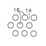
Fig. 2-9 show examples of patterns of interconnected conductive
dykes 14 which are separated by nonconductive islands 16, as may be
provided in a matrix which is used in a method according to the
first aspect. As is clearly apparent, the nonconductive islands 16,
which correspond to the openings which are to be formed, may adopt
various shapes and dimensions, even within a pattern.
The pattern depicted in Fig. 9 shows a grid with slot shaped
openings 16 between dykes 14, wherein the arrow 32 indicates the
orientation of high conductance of the conductor and arrow 30 of low
conductance of the conductor, respectively. Such a discrimination in
conductance by the pattern of the conductor is of interest when the
conductor is used in powertools and EV's, for instance.
The table I below shows the maximum open surface area as a
function of the number of holes/cmz for screen materials with a total
thickness of 20 micrometers which have been produced on an
electroforming matrix with a minimum dyke width of 15 micrometers and
a hexagonal grid, as shown in Fig. 2.
6
CA 02436244 2003-07-22
WO 02/061184 PCT/NL02/00064
Table I
Holes/cmz Mesh No. Dyke Skeleton Skeleton
Width Thickness Open
Matrix Surface
Area
(gym) (gym) Min. Max.
1 2.4 100 20 40 97
7.5 100 20 30 92
100 24 70 20 20 80
1000 75 30 20 10 63
10000 235 15 20 5 24
10000 235 15 10a 5 45
20000 335 15 20 3 7.5
20000 335 15 10a 3 30
a : further grown to 20 micrometers in a following step
Fig. 10 shows a graph representing this information. A
conductor according to the invention has a minimum value for the open
surface area (MIN. OPEN SURFACE AREA) in combination with a specific
thickness and mesh. number, since otherwise the advantages compared to
solid material are only marginal. The maximum value is determined by
the technique employed. As can be seen, the open surface area can be
increased, which offers advantages in particular for the higher mesh
numbers (generally a density of holes which is greater than or equal
to 10,000), by producing the screen material in two steps. Obviously,
even when using the two-step method, a conductor obtained has to
comply with the condition relating to the minimum open surface area.
The maximum open surface area (OA) can be calculated for a
screen material with a hexagonal grid by applying formula 1:
OA - (d-dyke-2*th)z 100 (1)
(d)z
wherein d = 25400 (gym)
mesh no.
dyke = dyke width (gym)
th - thickness of skeleton (gym)
The maximum open surface area is delimited by practical limitations.
7