Note: Descriptions are shown in the official language in which they were submitted.
CA 02436294 2003-07-31
-1-
PO'~ER OUTAGE ALERT ELECTR~lVf~C DE~7ICE
FIELD OF IN~IENTION
The present invention relates to devices for continuous monitoring power
delivery from a source to provide an alert that there has been a power outage.
More particularly, the present invention relates to power outage des~ices that
are
adaptable to a common power outlet, which provide an alert when there has been
one or more power outages and, further; which provide inforrrlation on the
outage,
e.g., the number of outages and the date, time, and duration of each outage,
and
the like.
DESCRIPTION OF THE RELATED ART
There has been a long standing need for sophisticated power outage
indicators for home use that are versatile, can be manufactured at low cost,
and
that are easy to install, operate, and maintain. For individuals who travel or
are
2 0 away from home for extended periods of time, it is important for them to
know
whether, in their absence, power has been interrupted ao that these
individuals can
prepare for, e.g., food spoilage, clocks that display an incorrect time, and
the like.
More specifically, there is a need for a reusable power outage indicator that
provides a visual display and/or an audible alarm and :provides meimory
st~rage for
a plurality of pov~~er outage events. However, devices fo:r detecting power
outages
for home and business use are known to the art.
For example, U.S. Patent Number 4,479, l 18 to Cole, Jr. teaches a power
3 0 outage indicator for use in locations that are not readily accessible. The
power
outage indicator of Cole, Jr. uses a liquid crystal display (LCI?) cell to
pro~~ide visual
indication that power has been interrupted. More speci.fcally, the L,CD cell
includes a pair of parallel electrodes between which is located a liquid
crystal
material. In manufacture, the cell is initially heated and an electric field
is
CA 02436294 2003-07-31
-2-
pro~~ided between the electrodes. As the cell is allowed to cool, the electric
field
causes the molecules of the liquid crystal material to assume first a homeotx-
opic
nematic orientation before the LCD cell reaches a smectic state. Vilhen the
LCD cell
is in a smectic state, the liquid crystal molecules align homeotropically,
producing
a clear exterior surface.
The Cole, Jr. power outage indicator also includes a current storing
capacitor that is connected in series through a switch to the pair of
electrodes. The
capacitor is in parallel with the source. As long as current flows from the
source,
the switch is closed. However, when a power outage interrupts the flow of
current,
the switch is opened and current stored in the capacitor is delivered to the
pair of
electrodes. The flow of current past the pair of electrodes produces heat,
which
heats the liquid crystal material above its clearing point temperature. As the
current and heat dissipate, the heated liquid crystal material cools. During
this
cooling process there is no electric field to align the ho:meotropic layers.
As a
result, cooling produces a different optical condition.
Problems with the Cole, Jr. power outage indicator include the complexity of
the indicator, a lack of memory, e.g., number, time, and duration of the
outage,
and an involved resetting process.
U.S_ Patent Number 4,466,074 to Jindrick, et al. teaches a power outage
timer that can be used in conjunction with a "smart" electronic watt-hour
meter to
record the duration of a power outage for the purpose of resetting the real-
time
2 5 value stored in the memory of the electronic watt-hour meter. The
electronic watt-
hour meter includes a microprocessor, a real-time value memory, and a clock
signal source.
According to the Jindrick patent, if there is a po~x~er outage, an outage
timer
3 0 causes a timing capacitor to discharge. After the outage is over, the time
it takes to
recharge the timing capacitor is measured. The microprocessor converts the
capacitor recharge time to a power outage time using look-up tables and a
driver
program. The microprocessor then adds the power outage time to the real-time
value to correct the time to account for the duration of the power outage.
CA 02436294 2003-07-31
-3-
SUMMARY OF THE INVENT10N
Accordingly, there is a need for a reusable power outage indicator that is
easy to use, install, and operate; that provides a visual display and audible
alarm of
any power outage events; and that provides memory storage for a plurality of
power
outage events to provide the date, time and duration of each power outage
event.
In one embodiment, the present invention provides a power outage detection
device for alerting users of the number, time, and duration of one or more
power
' outages, the deuce comprising:
a voltage input receiver for receiving voltage from a power source;
a voltage monitor for monitoring a reference voltage that is received from the
power source;
a change in voltage detector for detecting a change in the reference voltage,
wherein the change is determined by comparing the referezice voltage with a
threshold voltage and the change is of sufficient duration to constitute a
power
outage;
a microprocessor having a central processing unit;
2 0 a programmable real-time clock that is in comnnunication with the
microprocessor to provide current date and time data;
one or more input/output devices for communicating data to and from the
microprocessor, wherein the one or more input/output devices comprises at
least
one of:
a signal that is in communication with the microprocessor to indicate that
there has been one or more power outages;
a display that is in communication with the mi<:roprocessor to display data
on demand; and
an auxiliary energy power supply that provides power to the device during
3 0 the one or more power outages until the reference voltage exceeds the
threshold
voltage;
wherein the microprocessor comprises a plurality of memory that includes read
only memory for storing one or more microprocessor driver programs arid random
access memory for storing power outage data for one or more power outages.
CA 02436294 2003-07-31
BRIEF DESCRIPTION OF THE DRAWING
For a fuller understanding of the nature and desired objects of the present
invention, reference is made to the following detailed description taken in
conjunction with the accompanying drawing figures wherein like reference
characters denote corresponding parts throughout the several views and
wherein:
FIG. 1 shows a block diagram of an illustrative embodiment of a power
outage indicator in accordance with the present invention;
FIG. 2 shows an illustrative embodiment of a power outage indicator in
accordance with the present invention; and
FIG. 3 shows a flow chart of an illustrative embodiment of how a power
outage indicator works in accordance with the present invention.
DETAILED DESCRIPTION OF THE INVENTION AND THE PREFERRED
EMBODIMENTS THEREOF
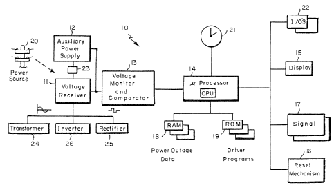
Referring now to the various figures, there are .~lzown in FIGs. 1 and 2,
respectively, a block diagram and an illustrative embodiment of a power outage
indicator 10 in accordance with the present invention The power outage
indicator
10 can detect power outage/failure and further can provide information about
one
2 5 or more power outages. The power outage indicator 10 includes a voltage
input
device 1 l, an auxiliary power supply 12, a voltage morzitor and cornparator
I3, a
microprocessor I4, one or more display devices I5, a reset mechanism I6, one
or
more input/output (I/O) devices 22, and one or more ;>ignaling devices 17.
3 0 Under normal operating conditions, which is to say, when there is no power
outage, the power source 20 delivers power to the power outage indicator 10
througkl the voltage input device 1 I. Preferably, the power source 20 is a
common
utility grid that delivers a standard 120-volt alternating current (AC) power.
More
preferably, the voltage input deuce I 1 comprises a pair of outlet prongs or
CA 02436294 2003-07-31
-5-
connectors and a ground prong that axe insertable in a common power outlet
(CPO), e.g., a standard 120-volt outlet or receptacle, through which power can
communicate from the power source 20 to the power outage indicator 10.
Because the voltage from the power source 20 exceeds the needs of the
power outage indicator 10 and may otherwise destroy the various components of
the power outage indicator I0, the voltage input device 11 can include a
transformer 24 to step down or reduce the voltage from 120 volts to about 12
volts
or less. Furthermore, the voltage input device 11 can include a rectifier 25
or an
inverter 26 to convert AC to DC.
In the event of a power outage, the power outage indicator 10 includes an
auxiliary power supply 12, e.g., a direct current (DC) battery, that is in
parallel with
the power source 20 to provide sufficient power to the various components of
the
power outage indicator 10. The auxiliary power supply 12 must be robust to
provide power at least for a predetermined period of time, which is to say,
for the
duration of a power outage that can last for several seconds or several hours.
Preferably, the predetermined period of time is at least two hours. More
preferably,
the predetermined period of time is at least six hours.
The voltage input device 11 communicates power from the utility grid 20 to a
voltage monitor and comparator 13. The purpcise of th.e voltage monitor and
comparator 13 is to monitor incoming voltage from the voltage input device 11
in
order to detect a decrease in the incoming voltage of sufficient magnitude to
cause
2 5 the voltage monitor and comparator 13 to switch circuits so that the power
to the
power outage indicator 10 comes from the auxiliary power supply I2 instead of
from the utility grid 20. The voltage monitor and cornparator 13 also monitors
.
incoming voltage from the voltage input device 11 in order to detect an
increase in
the incoming voltage of sufficient magnitude to cause the voltage monitor and
3 0 comparator 13 to switch circuits so that the power to t_~ne power outage
indicator 10
again comes .from voltage input device I l, i.e., the power source 20, instead
of from
the auxiliary power supply 12.
The microprocessor 14 comprises a central processing unit (CPU), random
CA 02436294 2003-07-31
access memory (RAM) 18, read-only memory (ROM) 19, and a real-time clock 21.
The ROM 19 includes a plurality of driver programs, i:.e., algorithms that
have been
reduced to a machine- or computer- readable source code, that can be called
and
executed by the CPU. The RAM 18 includes erasable memory for the temporary, or
volatile, storage of power outage data. For example, when incoming voltage
from
the voltage input device 11 decreases belo~r a reference voltage, the voltage
monitor
and comparator 13 can send a first signal to the CPU to invoke, or call, a
driver
program from the ROM 19 that will record the date and time of the power
outage,
which is on the real-time clock 21, and that will store that date and time
data in
memory, e.g., RAM 18, or a memory cache (not shown). Similarly, when incoming
voltage from the voltage input device 11 again increases above a reference
voltage,
the voltage monitor and comparator 13 can send a second signal to the CPU to
call
another driver program from memory, e.g., ROM 19, that will record the date
and
time of the power restoration; recall the pre~riously stored date and time
data of the
power outage; perform an operation on these data sets to calculate the elapsed
time
between power outage and restoration; and store the result of this calculation
in
memory, e.g., RAM 18 or a memory cache. The ROM 19 includes additional drivers
programs that respond to signals from other power outage indicator 10
components, e.g., the voltage monitor and comparator 13, the reset mechanism
16
and/or the I/O devices) 22, which will be described below.
The microprocessor 14 communicates with one or more I/O devices 22 to
enable a user to input data, e.g., the date, time or the mode of operation,
for use by
the microprocessor 14 and/or retrieve data from RAM 18, e.g., the number and
duration of power outages, or to Bail a driver program to be run by the
microprocessor 14. For example, one 1/O device can include a mode selector 31
that, when enabled, sends a signal to the microprocessor 14 to call a driver
program from ROM 19 that will allow the user to select an operating mode from
a
menu of modes that are stored in ROM 19, e.g., voltage: monitor mode, current
time
mode, clock set mode, set alarm mode, store outage date/time mode, store power
restored date/time mode, power outage (date and time) mode, power outage
(duration) mode, and the like. Another I/O device 22 c,an include an
hour/month/up scroll cursor input device 32, which allows a user to input the
hour of the day when operating in a clock set mode or the month of the year
when
CA 02436294 2003-07-31
_7_
operating in the date set mode or scroll through a menu upwards; and a
minute/day/down scroll cursor input deW ce 33, which allows a user to input
the
minute of the hour when operating in a clock set mode or the day of the month
when operating in the date set mode; or scroll through a menu downwards.
Yet another I/O device 22 that communicates vs~ith the microprocessor 14
can include a reset mechanism 16 that enables a user to reset input
information
vrhen operating in, e.g., a clock set mode, date set mode, alarm set mode, and
the
like and/or to purge data stored in memory, e.g., RAM 18, when operating in,
e.g.,
power outage (date and time) mode, power outage (duration) mode, and the like.
Accordingly, if, for example, the user makes a mistak~° when entering
the number
of minute past the hour when in the clock set mode, the user can activate the
reset
mechanism 16, which will send a signal to the CPU oil the microprocessor 14
invoking a driver program from memory, e.g., ROM 1 ~, that can erase the data
stored in the minute memory of the real-tune clock 21, thus allowing the user
to
input the correct number of minutes past the hour.
Preferably, the power outage indicator 10 of the present invention includes a
display device 15, e.g., a liquid crystal display (LCD) screen, a light
emitting diode
2 0 (LED) screen, and the like, for displaying data for any mode of operation.
For
example, normally, during the power monitor mode, the display device 15 will
output the current time, e.g., in hours, minutes with ~uz indication whether
AM or
PM. Similarly, when in a power outage (date and time rnode), the display
device 15
can output the date, e.g., by month and day, and/or time, e.g., by hour and
minute, of a power outage.
The power outage indicator 10 also can include a battery recharges 23 that
is in communication with the voltage input device 11 and with the auxiliary
power
supply 12. The battery recharges 23 makes it possible to recharge the
auxiliary
3 0 power supply 12 by storing power from the utility grid 20 in the auxiliary
power
supply 12 when power to the device 10 is being provideyd by the utility power
grid
20.
The power outage indicator 10 also includes a signaling device 15 to alert the
CA 02436294 2003-07-31
user that there has been a power outage jfailure. Preferably the signaling
device 15
is a visual, e.g., a strobe, flashing, e.g., red, light, steady, e.g., red,
light, light
emitting diode message, or liquid crystal display message and/or an audible
device,
e.g., a deW ce that produces a low frequency beeping or chirping noise.
Having described an embodiment of a power outage device 10, we will now
describe how the device 10 operates and the inter-relationship between the
components of the device 10. Referring to FIG. 3, there is shown a block
diagram
of the operation of a power outage device 10 in accordance with another
embodiment of the present invention. The device 10 is povrered by
communicating
the device with a power source 20, e.g., a utility grid. Preferably, the point
of
communication is a CPO, e.g., a standard 120-volt outlet or receptacle.
When the device 10 is connected for the farst time to a pow~°r
source 20 or
~~hen the de~~ice 10 has not been connected to a power source 20 for a period
of
time, and before the device 10 can be used to monitor power outages and
failures it
will be necessary to set the real-time clock 21. The real-time clock 21 can be
set by
selecting the time set mode after depressing the mode select device 31 and
then
entering the date and time. When the mode select device 31 is depressed, a
signal
2 0 is sent to the CPU, causing the CPU to invoke a mode menu driver program
that is
stored in memory, e.g., ROM 19. The mode menu driver program is executed by
the CPU, causing the operating modes of the mode menu to be sent to the device
10
for display one at a time on the display screen 15. Users can scro:tl through
the
operating modes of the mode menu using the up and down devices 32 arld 33.
After the user identifies the desired operating mode, e.g., the clock set
mode,
the user can double press the mode select device 31, which sends a signal to
the
CPU. ThlS Slgnal causes the mode menu driver program to shutdown and then
invokes a clock set driver program that is stored in memory, e.g., ROM 19. The
3 0 time set driver program is executed by the CPU, causing a month menu, day
menu,
and year menu to be sent to the det~iee 10 for display successively on the
display
screen 15.
The clock set driver program takes the user through the clock set algorithm
CA 02436294 2003-07-31
-9-
interactively by prompting the user to select the current month, day of the
month,
and year from corresponding month, day, and year menus using the up and down
buttons 32 and 33 to scroll through the respective menus.
For example, the CPU can communicate a current month menu to the
display device 15. After the user identifies the current month, the user can
double
press the mode select device 31, which sends a signal to the CPU t:o store the
data
in a real-time clock database and then transmit the days of the month menu to
the
display device 15. After the user identifies the current day of the month, the
user
can double press the mode select device 31, which sends a signal to the CPU to
store the data in the real-time clock database and the transmit the year menu
to
the display device 15. After the user identifies the current calendar year,
the user
can double press the mode select device 31, which ser~ds a signal to the CPU
to
store the data in the real-time clock database and transmit the hour of the
day
menu to the display device 15. After the user identifies the current hour of
the day,
the user can double press the mode select device 31, which sends a signal to
the
CPU to store the data in the real-time clock database and finally transmit the
minute of the hour menu to the display device 15. After the user identifies
the
current minute of the hour, the user can double press the mode select device
31,
2 0 which sends a signal to the CPU to store the data in a real-time clock
database. At
this point, the real-time clock 21 has been set to the current time and the
clock set
mode driver program is shut down. Preferably, the res~l-time clock 21 of the
present invention can include features that account for daylight savings time
and
leap years.
Once. the real-time clock 21 has been set, the device 1 D can be enabled to
monitor power outage/failure. To enable the voltage zrlonitor mode, users
again
can depress the mode select device 31. When the mode select devie:e 31 is
depressed, a signal is sent to the CPU, causing the CPU to invoke a mode menu
3 0 driver program that is stored in memory, e.g., ROM 19. The mode menu drive
program is executed by the CPU, causing the modes of the mode menu to be sent
to the display device 15 for display one at a time on the display screen I5.
Users
can scroll through the modes of the mode menu using the up and down devices 32
and 33.
CA 02436294 2003-07-31
- 10-
After the user identifies the desired operation mode, i.e., voltage monitor
mode, the user can double press the mode select device 31, which sends a
signal to
the CPU. This signal causes the mode men~cz driver program to shutdown and
then
invokes a voltage monitor driver program that is stored in memory, e.g., ROM
19.
The voltage monitor driver program is executed by the CPU, which causes a
power
outage counter to be set to zero, e.g., N = 0, STEP l and enables the voltage
monitor and comparator 13 to monitor voltage delivered to the voltage input
device
1 Z STEP 2.
The voltage monitor and comparator I3 monitors incoming voltage V;n and
compares the magnitude of the incoming voltage V;n with a reference or
threshold
voltage V~, STEP 3. As long as the incoming voltage Vv, exceeds the threshold
voltage V~,, the device IO continues to monitor the incoming voltage V~, STEP
2 and
voltage from the power source 20 powers the microprocessor 14 and the rest of
the
device 10. However, when the incoming voltage V;n dips below the threshold
voltage
V~,, the voltage monitor and comparator 13 sends one or more power outage
signals, e.g., to a switching device (not shov~n). The one or more power
outage
signals instantaneously switches the source of power to the device 10 from the
utility grid 20 to the auxiliary power supply 12 STEP 4a in a manner that is
well
2 0 known to the art.
The one or more signals from the voltage monitor and comparator 13 further
causes the CPU to increase the power outage event counter by one, e.g., N = N
+ l,
STEP 4b and invokes a store outage date/time driver ~>rogram STEP 4b that is
executed by the CPU. The invoked store outage date/time driver program
instantaneously reads the current date and time of the: real-time clock 21.
These
data, i.e., power out date and time, are then stored in memory, e.g., ROM 18,
STEP
4c. The one or more signals also can enable the at leaat one signaling device
17
STEP 4d to provide a visual and/or audible signal to alert the user that there
has
3 0 been a power outage.
The voltage monitor and comparator 13 continues to monitor incoming
voltage V~, and compares the magnitude of the incoming voltage V~, with the
threshold voltage V~r, STEP 5. As long as the incoming voltage V;~ i;s less
than the
CA 02436294 2003-07-31
-11-
threshold voltage V~,, voltage from the auxiliary power supply 12 powers the
microprocessor 14 and the rest of the device 10. However, when the incoming
voltage V~, exceeds the threshold voltage V~,, the voltag~° monitor and
comparator
13 sends one or more power outage signals, e.g., to the switching device STEP
6.
The one or more power outage signals instantaneously switches the source of
power to the device 10 back to the utility grid 20 STEP r c.
The one or more signals from the voltage monitor and comparator 13 also
invokes a store power restored time driver program that is stored in memory,
e.g.,
ROM 19. The invoked store power restored date/time driver program
instantaneously reads the current date and time of the real-time clock 21.
These
data, i.e., power restored date and time, are then stored in memory, e.g., RAM
18,
or, alternatively, in a memory cache STEP 7a. The store power restored time
driver
program also can calculate the amount of time between the power outage and
power restoration (fit) STEP 7b and, further, can store chat data and the
outage
event counter number N in memory, e.g., RAM 18.
Once the device 10 has been through a power outage-power restoration
cycle, the device 10 can return to the monitor voltage mode STEP 2 until the
user
2 0 disables the monitor voltage mode STEP 8. To disable the voltage monitor
mode,
the user can depress the mode selection device 31, which produces a scrollable
menu of device operating modes that has been described previously. For
example,
the user can select a date and time of power outage made and/or a number and
duration of power outages mode. Alternatively, the user can depress a reset
2 5 mechanism 16, which will automatically disable the at least one signaling
device 17
STEP 9 and terminate the voltage monitor mode.
After the user identifies the desired operation mode, e.g., the power outage
(date and time) mode or the power outage (number and', duration) mode, the
user
30 can double press the mode select device 31, which sends a signal to the
CPU. This
signal causes the mode menu driver program to shutdown and also invokes a
power outage (date and time) driver program or a power outage (nu:mber and
duration) driver program that are stored in memory, e.g., ROM 19. The power
outage (date and time }or power outage (number and duration) driver program is
CA 02436294 2003-07-31
- 12-
then executed by the CPU.
The power outage (date and time) driver program, for example, causes the
CPU to read the data, i.e., time T; and date D; for each power outage event l
= 1, . .
., N, that ~~ere stored in memory, e.g., RAM 18, STEP 10 and display that data
on
the display device I5 STEP 11 on demand. Similarly, the power outage (number
and duration) driver program causes the CPU to read t:he data, i.e., number N
and
duration of each power outage ~t; for l = 1, . . . N, that ~raere stored in
memory, e.g.,
RAM 18, STEP 10 and display the data on the display device 15 STEP 11 on
demand.
,Although preferred embodiments of the invention have been described using
specific terms, such descriptions are for illustrative purposes only, and it
is to be
understood that changes and variations may be made ,without departing from the
spirit or scope of the following claims.
For example, the power outage device 10 also can include an alarm clock
feature that will allow the user to input an alarm on time through a set alarm
mode. After the user selects the set alarm mode, a set alarm driver program
that is
2 0 stored in memory, e.g., ROM 19, can be invoked. Preferably, the set alarm
driver
program can lead the user through the same sequence of steps and entries as
previously described for setting the real-time clock 21. Once the alarm time
is set,
e.g., after double pressing the mode selection button 31, the device 10 can
operate
in an alarm clock mode. When the time on the real-time clock 21 reaches the
2 5 alarm set time, the CPU sends a signal enabling at leap>t one of the
signaling
devices 17. The signaling device I7 continues to provide a visual or audible
signal
until the user enables the reset mechanism 16, which causes the device 10 to
return to the default mode, i.e., curx-ent time mode. Alternatively, the
signaling
device 17 can be programmed in advance to stop after a certain period of time.
Although the invention has been described havis~ag a utility grid as a power
source, the invention is not to be construed as being so ii'rrm?ted. Those
skilled in
the art can appreciate that the power source 20 can include a fuel cell,
flywheel
assembly, induction-type motor, diesel motor, energy storage device, and the
like.