Note: Descriptions are shown in the official language in which they were submitted.
CA 02436709 2003-07-29
-1-
SPECIFICATION
OPTICAL CONTROL 1VIETHOD AND DEVICE
TECHNICAL FIELD
The present invention relates to optical function
elements for amplification, control or switching of optical signals,
and more particularly to optical control method and device
suitable for photoelectronics such as optical communication,
optical image processing, optical computation, optical
measurement and optical integrated circuits, which are capable
of advanced information processing.
BACKGROUND ART
There have been demanded extensive developments
of broad-band services such as dynamic image communication
and picture image transmission or distribution, using fiber-optic
communication capable of broad-band efficient data transmission
or transfer. In electronics, for example, there have not yet been
realized functional elements (active elements) equivalent to
triode transistors, that is, optical function elements capable of
controlling an optical signal directly with another optical signal.
Actually, therefore, an optical signal that has been
transmitted at a high-speed is once converted into an electrical
signal, which is subjected to data processing in an electronic
circuitry, and the processed data signal is then reconverted into
an optical signal to be transmitted. This incapability to achieve
CA 02436709 2003-07-29
.~. ,
direct control of an optical signal with another optical signal has
limited the efficiency of optical signal processing. If a data
signal can be processed as received in the form of an optical
signal, it is considered possible to perform parallel processing
operations, which are expected to permit further reduction in the
required signal processing time.
DISCLOSURE OF INVENTION
The present invention was made in the light of the
background art described above. It is an object of the present
invention to provide optical control method and device which
permit processing of an optical signal directly with another
optical signal.
In the light of the background art described above,
the present inventor has made extensive studies, and found out
that a spontaneous emission light generated from a fiber
amplifier (optical amplifying element) doped with a rare earth
element, which light has a wavelength near a wavelength y of
an input light incident upon the fiber amplifier, has a response to
a variation in the intensity of that input light, and that a
variation in the intensity of the spontaneous emission light is
reversed with respect to the variation in the signal intensity of
the input light. The inventor has also found out a phenomenon
that if a laser light having another wavelength ~,~~ within the
wavelength band of the spontaneous emission, that is, within a
neighboring wavelength band of the input light, is coupled with
the input light, the overall intensity of the spontaneous emission
CA 02436709 2003-07-29
.3.
is abruptly increased while the variation in the signal
(amplitude) of the spontaneous emission is maintained. Namely,
the inventor has found out a laser inducted signal enhancement
effect. Further, the present inventor has found out that a
phenomenon similar to that described above is obtained not only
in a semiconductor optical amplifying element, but also in a case
where the light having the wavelength y is selectively output
from the light generated within the semiconductor optical
amplifying element, rather than the laser light having the
wavelength ~,~~ is coupled with the input light. These
phenomena are considered to be wavelength conversion from the
wavelength y to the wavelength ~,~~. The inventor has conceived
Tandem Wavelength Conversion Optical Triode, based on tandem
wavelength conversion in which the wavelength conversion is
effected in tandem connection, and has arrived at the optical
control method and device based on this conception. The
present invention was made on the basis of the findings
described above.
That is, there is provided according to the invention
corresponding to appended claim l, a first optical control method
comprising (a) a step of inputting a first input light of a first
wavelength to a first optical amplifying element, so that a light
having a wavelength within a wavelength band which includes
the wavelength of said first input light and in which the first
optical amplifying element has an amplification gain is
intensity-modulated in response to a variation in an intensity of
said first input light, (b) a step of inputting to the first optical
CA 02436709 2003-07-29
~. ,
amplifying element a laser light of a second wavelength within
the wavelength band in which said first optical amplifying
element has the amplification gain, (c) a step of extracting the
light of the second wavelength from a light generated from said
first optical amplifying element, and inputting the extracted light
to a second optical amplifying element, (d) a step of inputting to
said second optical amplifying element a laser light of said first
wavelength or a laser light having a third wavelength within a
wavelength band which includes the first wavelength and in
which said second optical amplifying element has an
amplification gain, and (e) a step of extracting the light of said
first or third wavelength from a light output from said second
optical amplifying element, and outputting the light of the first
or third wavelength.
The optical control method described above is
preferably practiced by an optical control device corresponding to
appended claim 5, which comprises (a) a first optical amplifying
element operable to receive a first input light of a first
wavelength and intensity-modulate a light having a wavelength
within a wavelength band which includes the wavelength of said
first input light and in which the first optical amplifying element
has an amplification gain, such that the light having the
wavelength within the above-indicated wavelength band is
intensity-modulated in response to a variation in an intensity of
the first input light, (b) a first optical inputting element operable
to input to said first optical amplifying element a laser light of a
second wavelength within the wavelength band in which the first
CA 02436709 2003-07-29
.5.
optical amplifying element has the amplification gain, (c) a first
optical filtering element operable to extract the light of the
second wavelength form a light output from said first optical
amplifying element, (d) a second optical amplifying element
operable to receive the light of the second wavelength extracted
by said first optical filtering element, and intensity-modulate a
light having a wavelength within a wavelength band which
includes said second wavelength and in which the second optical
amplifying element has an amplification gain, such that the light
having the wavelength within the wavelength band including the
second wavelength is intensity-modulated in response to a
variation in an intensity of the second input light, (e) a second
optical inputting element operable to input to the second optical
amplifying element a laser light of said first wavelength or a
laser light of a third wavelength within the wavelength band
which includes the first wavelength and in which the second
optical amplifying element has the amplification gain, and (f) a
second optical filtering element operable to extract the light of
the first or third wavelength from a light output from the second
optical amplifying element, and output the light of the first or
third wavelength.
The optical control method and device described
above are three-terminal control method and device capable of
amplification and switching of an optical signal by using another
optical signal. Namely, when the first optical amplifying
element receives the second input light (laser light) of the second
wavelength within the wavelength band in which the first optical
CA 02436709 2003-07-29
_6_
amplifying element has an amplification gain to
intensity-modulate the surrounding light of the first input light
in response to a variation in the intensity of the first input light,
the amplified light of the second wavelength is extracted and
input to the second optical amplifying element. When the
second optical amplifying element receives a third input light of
the third wavelength (or first wavelength) within the wavelength
band in which the second optical amplifying element has an
amplification gain to intensity-modulate the surrounding light of
the amplified light of the second wavelength in response to a
variation of this amplified light, the output light of the third
wavelength (or first wavelength) is generated from the optical
control device. This output light is switched and amplified in
synchronization with the third input light.
The object indicated above is achieved according to
the invention defined in appended claim 2, that is, by a second
optical control method comprising (a) a step of inputting a first
input light of a first wavelength to a first semiconductor optical
amplifying element, so that a light generated within the first
semiconductor optical amplifying element is intensity-modulated
in response to a variation in an intensity of said first input light,
(b) extracting the light of a second wavelength from a light which
is generated within said first semiconductor optical amplifying
element and which has the second wavelength within a
wavelength band in which said first semiconductor optical
amplifying element has an amplification gain, and outputting the
extracted light to a second semiconductor optical amplifying
CA 02436709 2003-07-29
. ! .
element, (c) a step of inputting to the second semiconductor
optical amplifying element a laser light of said first wavelength
or a laser light of a third wavelength within a wavelength band
which includes the first wavelength and in which the
above-indicated second semiconductor optical amplifying element
has an amplification gain, and (d) a step of extracting the light of
the first or third wavelength from a light output from said second
semiconductor optical amplifying element, and outputting the
light of the first or third wavelength.
The second optical control method described above
is preferably practiced by an optical control device corresponding
to appended claim 6, which comprises (a) a first semiconductor
optical amplifying element operable to receive a first input light
of a first wavelength and intensity-modulate a light having a
wavelength within a wavelength band which includes the
wavelength of said input light and in which said first
semiconductor optical amplifying element has an amplification
gain, such that the light having the wavelength within the
wavelength band is intensity-modulated in response to a
variation in an intensity of the first input light, (b) a first optical
inputting element operable to input the light of said first
wavelength to said first semiconductor optical amplifying
element, (c) a first optical filtering element operable to extract a
light of a second wavelength from a light which is generated
within the first semiconductor optical amplifying element and
which has the second wavelength within a wavelength band in
which the first semiconductor optical amplifying element has an
CA 02436709 2003-07-29
_8_
amplification gain, and output the extracted light as an output
light, (d) a second semiconductor optical amplifying element
operable to receive the light of the second wavelength extracted
by the first optical filtering element, and intensity-modulate a
light having a wavelength within a wavelength band which
includes the second wavelength and in which the second
semiconductor optical amplifying element has an amplification
gain, such that the light having the wavelength within the
wavelength band including said second semiconductor
wavelength is intensity-modulated in response to a variation in
an intensity of said second input light, (e) a second optical
inputting element operable to input to said second semiconductor
optical amplifying element a laser light of said first wavelength
or a laser light of a third wavelength within the wavelength band
which includes the first wavelength and in which the
above-indicated second semiconductor optical amplifying element
has the amplification gain, and (f) a second optical filtering
element operable to extract the light of the first or third
wavelength from a light output from said second semiconductor
optical amplifying element, and output the light of the first or
third wavelength.
The optical control method and device described
above are three-terminal control method and device capable of
amplification and switching of an optical signal by using another
optical signal. Namely, the first optical amplifying element
outputs the amplified light of the second wavelength which lies
within the wavelength band in which the first optical amplifying
CA 02436709 2003-07-29
-9-
element has an amplification gain for intensity-modulation in
response to a variation in the intensity of the first input light,
and the amplified light of the second wavelength is extracted and
input to the second optical amplifying element. When the
second optical amplifying element receives a second input light of
the third wavelength (or first wavelength) within the wavelength
band in which the second optical amplifying element has an
amplification gain for intensity-modulation in response to a
variation of this amplified light, the output light of the second
wavelength (or first wavelength) is generated from the optical
control device. This output light is switched and amplified in
synchronization with the second input light.
The object indicated above is achieved according to
the invention defined in appended claim 3, that is, by a third
optical control device comprising (a) an optical amplifying
element operable to receive an input light of a second wavelength
and intensity-modulate a light having a wavelength within a
wavelength band which includes the wavelength of said input
light and in which the optical amplifying element has an
amplification gain, such that the light having the wavelength
within the above-indicated wavelength band is
intensity-modulated in response to a variation in an intensity of
said input light, (b) an optical inputting element operable to
input to the optical. amplifying element a light of a first
wavelength within the wavelength band in which the optical
amplifying element has the amplification gain, and (c) an optical
filtering element operable to extract the light of said first
CA 02436709 2003-07-29
1~
wavelength from a light output from said optical amplifying
element, and outputting the extracted light of said first
wavelength as an output light.
In the optical control device, the laser light of the
first wavelength is input to the optical amplifying element which
is arranged to intensity-modulate the light of the wavelength
within the wavelength band which has the wavelength of the
input light and in which the element has an amplification gain.
As a result, an amplified light of the first wavelength within the
above-indicated wavelength band is generated as an output light,
which is an amplified signal whose waveform is reversed with
respect to that of the first input light.
The object indicated above is also achieved by a
fourth optical control device corresponding to appended claim 4,
which comprises (a) a semiconductor optical amplifying element
operable to receive an input light of a first wavelength and
intensity-modulate a light having a wavelength within a
wavelength band which includes the wavelength of said input
light and in which the semiconductor optical amplifying element
has an amplification gain, such that the light having the
wavelength within the above-indicated wavelength band is
intensity-modulated in response to a variation in an intensity of
said input light, (b) an optical inputting element operable to
input to the semiconductor optical amplifying element a light of
the first wavelength within the wavelength band in which the
semiconductor optical amplifying element has the amplification
gain, and (c) an optical filtering element operable to extract the
CA 02436709 2003-07-29
11
light of said second wavelength from a light generated within the
optical amplifying element, and output the extracted light of said
second wavelength as an output light.
In the optical control device described above, the
optical amplifying element is arranged to intensity-modulate a
light of a wavelength within the wavelength band which includes
the wavelength of the input light and in which the optical
amplifying element has an amplification gain, such that the light
of the wavelength within the above-indicated wavelength band is
intensity-modulated in response to a variation in the intensity of
the input light. The laser light of the second wavelength within
the above-indicated wavelength band is extracted from the light
output generated within the optical amplifying element.
Accordingly, the amplified light of the second wavelength within
the above-indicated wavelength band is obtained as an output
light, which is an amplified signal whose waveform is reversed
with respect to that of the first
Preferably, the optical amplifying element is an optical fiber
doped with a rare-earth element. In this case, the coupled lights
of the first and second wavelengths are easily input to one end of
the fiber amplifier, and output from the other end of the fiber
amplifier. The optical amplifying element is a glass fiber which
is doped with a high concentration of erbium and which is excited
by an excitation light having a wavelength permitting optical
absorption at the normal energy level, for example, a wavelength
of 0.98~,m or 1.48ym. In this instance, the doping of the glass
fiber with the high concentration of erbium reduces the lifetime
CA 02436709 2003-07-29
' l~ .
of the spontaneous emission energy level, permitting a
high-speed operation of the optical amplifying element.
Preferably, the semiconductor optical amplifying
element is a semiconductor optical amplifying element operable
to generate a light from its pn-junction portion, namely, its active
layer (light~emitting layer) upon application of an electric current
thereto. In this case, the optical amplifying element can be
small-sized, and the switching speed of the element can be
increased. The semiconductor optical amplifying element is
desirably constituted by one of a semiconductor optical
amplifying element of traveling-wave type (SOA) whose opposite
end faces are processed to prevent optical reflection, a
semiconductor optical amplifying element of Fabry-Perot type
whose opposite end faces cooperate to define an optical resonator,
a semiconductor optical amplifying element of distributed
feedback type, a semiconductor optical amplifying element of
distributed Bragg reflector type, a semiconductor optical
amplifying element of external-resonance type, and a
semiconductor optical amplifying element of surface-emitting
type. The active layer providing the pn-junction portion is
preferably constituted by one of a quantum well, a quantum slit,
a quantum chamber and a strained superlattice.
Preferably, the optical filtering element is a grating
filter constituted by an optical fiber or waveguide having a
portion a refractive index of which is periodically changed in a
longitudinal direction thereof. Where the optical control device
per se is constituted by an optical fiber or waveguide, the
CA 02436709 2003-07-29
-13-
above-indicated grating filter may consist of a portion or the
entirety of the optical fiber or waveguide. In this case, the
optical control device can be further small-sized.
The optical filtering element is preferably an optical
filtering portion of the optical control device, which is provided by
forming alternate projections and recessed periodically on a
surface of a waveguide in the longitudinal direction. In this case,
the waveguide need not be given a periodic change of its
refractive index, so that the optical control device can be easily
integrated as a monolithic IC.
Preferably, the optical filtering element is
constituted by a multiplicity of layers which are superposed on
each other and which having respective different refractive index
values, to selectively permit transmission or reflection of light of
a predetermined wavelength. This arrangement is effective
particularly where the optical control device is operated with a
surface-emitting semiconductor laser.
The optical inputting element is desirably
constituted by one of an optical coupler, a directional coupler and
an optical circulator. Where the optical circulator is used, the
first input light can be input from an output portion of a
semiconductor laser, which is commercially available and
inexpensive.
BRIEF DESCRIPTION OF DRAWINGS
Fig. 1 is block diagram illustrating an arrangement
of an optical control device according to one embodiment of the
CA 02436709 2003-07-29
14-
present invention.
Fig. 2 is a view for explaining an energy level
arrangement of an optical amplifying element in the embodiment
of Fig. 1.
Fig. 3 is a view for explaining a spectrum of a
spontaneous emission generated based on an input light, in the
optical amplifying element in the embodiment of Fig. 1.
Fig. 4 is a view indicating a spectrum including a
component having a wavelength ~.1 selected by an optical filtering
element from the spontaneous emission generated in the optical
amplifying element based on a second laser light Lz having a
second wavelength ~.z, in the optical control device of Fig. 1,
wherein the spectrum where a first laser light L1 having a first
wavelength ~,1 is not coupled with the second laser light La is
indicated at (a), while the spectrum where the first laser light Ll
is coupled with the second laser light L~~.
Fig. 5 is a view showing intensity I~~ of the input
light of the second wavelength ~,z and intensity Iout of an output
light of the wavelength y, in comparison with each other, with
their signal waveforms taken along a common axis of time, in the
optical control device of Fig. 1.
Fig. 6 is a view showing intensity of I~~ of the input
light and intensity Iout of the output light, in comparison with
each other, with their signal waveforms taken along the common
axis of time, where the first laser light L1 of the wavelength hl
which is coupled with the intensity I~ of the input light of the
second wavelength ~.~~ is modulated, in the optical control device
CA 02436709 2003-07-29
15,
of Fig. 1.
Fig. 7 is a view illustrating an arrangement of an
optical control device according to another embodiment of this
invention.
Fig. 8 is a view showing input and output
waveforms in the embodiment of Fig. 7 taken along a common
axis of time, in comparison with each other.
Fig. 9 is a view illustrating an arrangement of an
optical control device according to a further embodiment of this
invention.
Fig. 10 is a view showing input and output
waveforms in the embodiment of Fig. 9 taken along a common
axis of time, in comparison with each other.
Fig. 11 is a view indicating a relationship between
an input light intensity and an output light intensity, for
different control lights used as a parameter, in the embodiment
of Fig. 9.
Fig. 12 is a view illustrating an arrangement of an
optical control device according to a yet further embodiment of
this invention.
Fig. 13 is a view illustrating an arrangement of an
optical control device according to a still further embodiment of
this invention.
Fig. 14 is a perspective view illustrating
arrangements of semiconductor optical amplifying elements in
the optical control device in the embodiment of Fig. 13, wherein
the amplifying element in the form of a DFB semiconductor layer
CA 02436709 2003-07-29
-16-
element is indicated at (a), while the amplifying element in the
form of a DBR semiconductor laser element is indicated at (b).
Fig. 15 is a view showing a waveform of an input
light and a waveform of an output light, to explain an operation
of the optical control device in the embodiment of Fig. 13
Fig. 16 is a view illustrating an arrangement of an
optical control device according to another embodiment of the
present invention.
Fig. 17 is a view showing a waveform of an input
light and a waveform of an output light, to explain an operation
of the optical control device in the embodiment of Fig. 16.
Fig. 18 is a view illustrating an arrangement of an
optical control device according to a further embodiment of this
invention.
Fig. 19 is a view showing a waveform of an input
light and a waveform of an output light, to explain an operation
of the optical control device in the embodiment of Fig. 18.
CA 02436709 2003-07-29
1. l
BEST IiIODE FOR CARRYING OUT THE INVENTION
Referring to the drawings, there will be described in
detail an optical control device 10 according to one embodiment of
this invention.
In Fig. l, there is shown a first laser light source 12,
which is arranged to generate a first laser light L~ having a first
wavelength y, for example, 1534nm, such that the generated
first laser light L~ propagates through a first optical fiber F1 to a
first optical modulator 14. A second laser light source 16 is
arranged to generate a second laser light L~~ having a second
wavelength ~.~~, for example, 1555nm, such that the generated
second laser light L~~ propagates through a second optical fiber F
to a second optical modulator 18. For instance, the first laser
light source 12 and the second laser light source 16 are
variable-wavelength semiconductor lasers. The first optical
modulator 14 and the second optical modulator 18 are arranged
to effect pulse modulation of the laser lights passing
therethrough, according to electric signals generated from
respective signal generators 20, 22, so that the laser lights are
modulated into pulse signals having respective frequencies of the
electric signals. An optical coupler 24 connects the
above-indicated first optical fiber Fi and second optical fiber Fz to
a third optical fiber Fs, and couples the first and second laser
lights L1, L~~ which have propagated through the respective first
and second optical fibers F1, Fz. The coupled laser lights L1, L
are input to an optical amplifying element 2F through the third
CA 02436709 2003-07-29
_ I8'
optical fiber F3. An optical filtering element 28 is connected to
the optical amplifying element 26, and is arranged to extract a
light of the first wavelength ~,l from the light output from the
optical amplifying element 26, and output the extracted light as
an output light. Those optical amplifying element 26 and
optical filtering element 28 correspond to the optical control
device 10 which converts the signal of the second laser light L
into a signal of the wavelength ~,1, and directly amplifies the
latter signal into the output light. In Fig. 1, there are also
shown a pair of photodetectors 30, 32 arranged to monitor the
output light that has passed through the optical filtering element
28, and the coupled first and second laser lights L1, L~~, and an
oscilloscope 34 for observing optical signals as detected by the
photodetectors 30, 32.
For example, the optical amplifying element 26
described above is a light-transmitting medium such as quartz or
fluoride glass, which is doped with a rare-earth element such as
erbium, so as to establish three- or four-energy-level system
within the light-transmitting medium, as indicated in Fig. 2,
thereby forming a so-called "laser system". The optical
amplifying element 26 in the present embodiment is constituted
by a glass fiber which has a length of about 20m and which is
doped with erbium and aluminum and includes erbium ion Er3+
of a comparatively high concentration of about 1700ppm and
aluminum ion Al3+ of about 10000ppm. In this respect, the
optical amplifying element 26 is also referred to as an
erbium.-doped fiber amplifier (EDFA). This optical amplifying
CA 02436709 2003-07-29
.19_
element 26, when it is placed in its excited state, is capable of
optically amplifying the light of the above-indicated first
wavelength ~.1 or second wavelength ~,~~. When a laser light of a
wavelength of 1.48ym, for example, is propagated in the
longitudinal direction of the optical amplifying element 26, the
erbium element is kept in its excited state, so that upon incidence
of either of the above-indicated wavelengths, for instance, the
second wavelength ~.p, there is generated a broad-band
spontaneous emission light (ASE) having the second wavelength
W as its center wavelength, as shown at (a) in Fig. 3. Further,
increasing the intensity of the laser light of the second
wavelength ~,~ causes a phenomenon that the intensity at the
center wavelength is increased, while on the other hand the
intensity of the light in the neighboring wavelength band is
reduced, as shown at (b) in Fig. 3. The above-indicated
spontaneous emission light, that is, the surrounding light has a
wavelength band in which the optical amplifying element 26 has
an amplification gain.
For example, the optical filtering element 28
described above is a fiber grating filter formed of a glass filter
which is locally irradiated with a ultraviolet radiation and the
refractive index of which is locally periodically changed in its
longitudinal direction. The optical filtering element 28 extracts
and passes the light having the first wavelength ~,1 as the center
wavelength and a half-width value of lnm. For instance, the
optical filtering element 28 is provides at the terminal portion of
the glass filter of the optical amplifying element 26 described
CA 02436709 2003-07-29
?o
above.
When only the modulated second laser light Lp is
input to the optical amplifying element 26 in the optical control
device 10 arranged as described above, the output light extracted
by the optical filtering element 28 has a spectrum as shown at (a)
in Fig. 4. When the second laser light L~~ coupled with the
non-modulated first laser light L1 is input to the optical
amplifying element 26, the output light extracted by the optical
filtering element 28 has a spectrum as shown at (b) in Fig. 4.
The output lights shown at (a) and (b) in Fig. 4 are the
wavelength L1 components which have been extracted by the
optical filtering element 28 from the spontaneous emission light
generated within the optical amplifying element 26 upon
incidence of the second laser light L~~ of the second wavelength ~,z.
In the case shown at (b) in Fig. 4 wherein the non-modulated
first laser light L1 is coupled with the second laser light Lz, the
peak intensity value of the output light is considerably increased
owing to the laser induced signal enhancement effect described
above. The non-modulated light is interpreted to mean a
continuous wave having a constant intensity.
In the optical control device 10 of Fig. l, therefore,
the second laser light L~~ is modulated at lkHz by the second
modulator 18, and the thus modulated second laser light Lz (Iz)
coupled with the non-modulated first laser light L1 (Ii) is input to
the optical amplifying element 26, so that the lkHz input signal
(second laser signal La) indicated at (c) in Fig. 5 is amplified into
an output light (IOUr.) indicated at (a) in Fig. 5. At (b) in Fig. 5,
CA 02436709 2003-07-29
' 71'
there is shown an output light when the non-modulated first
laser light L~ is not coupled with the modulated second laser light
L~~ input to the optical amplifying element 26. The intensity Io~,t.
of the above-indicated output light measured by an optical power
meter was 273mW when the intensity I1 was O~.W, and 1350yW
when the intensity I1 was SmW. It is apparent from this fact
that the intensity Iout of the output light is considerably
amplified by coupling the first laser light Ll with the second laser
light Lz. It is also noted that the waveform of the output light is
reversed with respect to that of the input light, and that the
percentage (%) of modulation of the input light is held constant.
The modulation percentage is represented by 100 x (Imam -
Imin)/(Ima, + Ian), where "Imam" represents a maximum value of the
optical signal while "Imin" represents a minimum value of the
optical signal.
In the optical device 10 including the
above-described optical amplifying element ~6 and optical
filtering element 28, a second input light in the form of the
second laser light Lp having the second wavelength ~,z is input to
the optical amplifying element 26, and a first input light having
the first wavelength ~,1 which is different from the second
wavelength ~,z is input to the optical amplifying element 26
through the optical coupler 24 functioning as an optical input
device or element. The first wavelength ~,1 is selected within a
wavelength band of the surrounding light (spontaneous emission
light) with respect to the second wavelength ~,~~, that is, within
the neighboring wavelength band of the second input light.
CA 02436709 2003-07-29
. 77 .
Thus, the second laser light L~~ and the first laser light L1 are
coupled together, and the light output from the optical amplifying
element 26 is filtered by the optical filtering element 28, to
output an output light having the first wavelength y. This
output light is amplified in response to a signal variation of the
second laser light La of the second wavelength ~,z, so that the
signal variation of the second laser light Lz is amplified. Namely,
the output light, which has a phase reversed with respect to the
input signal in the form of the modulated second laser light L~,
has the signal intensity Iour which is considerably amplified with
respect to the signal intensity I~~ of the second laser light L~~.
The optical amplifying element 26 used in the
present embodiment is constituted by a glass fiber doped with
erbium, for example, and is arranged to receive at one end of the
glass fiber the first laser light L~ and second laser light L~~ which
have been coupled together, and generates the output light at the
other end of the glass filter, which can be easily filtered by the
optical filtering element 28. Further, the glass filter of the
optical amplifying element 26 which is doped with a high
concentration of erbium is excited by an incident excitation light
having a wavelength permitting optical absorption at the normal
energy level, for example, a wavelength of 0.98ym or 1.48~.m.
The doping of the glass fiber with the high concentration of
erbium reduces the lifetime of the spontaneous emission energy
level, permitting a high-speed operation of the optical amplifying
element 26.
On the other hand, the optical filtering element 28
CA 02436709 2003-07-29
.
used in the present embodiment also functions as an optical
output element or device, and is a grating filter constituted by a
glass filter the refractive index of which is locally periodically
changed in its longitudinal direction. The grating filter of the
optical filtering element 28 may be constituted by a portion of the
glass filter of the optical amplifying element 26, or by a glass
filter connected to the glass filter of the element 26, so that the
optical amplifying device 10 functioning as an optical function
element can be small-sized.
Other embodiments of the present invention will be
described. In the following description, the same reference signs
as used in the above embodiment will be used to identify the
functionally corresponding elements, which will not be described
redundantly.
Referring to Fig. 6, there are illustrated waveforms
where an input light is modulated at 20kHz by the first
modulator 14 in the device of Fig. 1. Fig. 6 shows at (a) an input
light (second laser light Lz) subjected to the 1 kHz modulation,
and shows at (b) an output light (Iouc.) obtained as a result of
coupling of the input light in the form of the second laser light L
and the input light (first laser light L1) subjected to the 20 kHz
modulation. This embodiment is a case where the signal
frequency is relatively low. Namely, it is confirmed that
sufficient amplification of the input light is where the modulation
frequency of the first laser light L 1 is on the order of giga Hz. It
is also noted that switching of the output light is possible, by
setting a suitable threshold value T as indicated in Fig. 6.
CA 02436709 2003-07-29
. y .
Fig. r shows an optical control device 38 which uses
two optical control devices identical with the optical control
device 10 used in the embodiment of Fig. l, to provide a pair of
optical switches. In the device of Fig. 7, a pair of optical
amplifying elements 26, 26' are adapted to receive a modulated
signal of the wavelength y generated by the laser light source 12
as indicated at (1) in Fig. 8, and respective two modulated signals
of the wavelength ~,~~ and having mutually reversed phases
generated by the respective laser light sources 16, 16' as
indicated at (2) and (4) in Fig. 8. The modulated signal of the
wavelength ~.1 is coupled with the modulated signals of the
wavelength ~,~~, by the respective optical couplers 24, 24'. A pair
of optical filtering elements 28, 28' are adapted to receive the
coupled modulated signals and extract the first wavelength ~,1,
thereby outputting a pair of output lights as indicated at (3) and
(5) in Fig. 8. Thus, the modulated first input laser light having
the wavelength ~,1 is switched into the two output lights, by the
modulated second input laser light having the wavelength y.
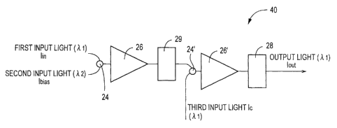
Fig. 9 shows an optical control device 40 wherein
the first optical coupler 24 is adapted to couple together a first
laser light L1 of the wavelength y (first input light: hn) and a
second laser light L~~ of the wavelength ~,~~ (second input light or
bias light Ibia~), which are input to the optical amplifying element
26, and a first optical filtering element 29 is adapted to extract
the wavelength ~,~ of the output of the optical amplifying element
26. Further, the second optical coupler 24' is arranged to couple
the output light of the first filtering element 29 and a third laser
CA 02436709 2003-07-29
light La of the wavelength ~.1 in the form of a non-modulated,
continuous wave signal (third input light or control light I~).
The output of the second optical coupler 24' is input to the second
optical amplifying element 26', and a second optical filtering
element 28 is adapted to extract the wavelength y of the output
of the second optical amplifying element 26', for thereby
outputting an amplified output signal Io«c as indicated at (a) in
Fig. 10. Fig. 10 shows at (b) an optical output signal where the
third laser light L,3 is not coupled with the output of the
wavelength ~,~~ of the optical filtering element 29, when the output
of the optical filtering element 29 is input to the second optical
amplifying element26'. Fig. 10 shows at (c) a signal waveform of
the above-indicated first laser light Ll.
Fig. 11 indicates an input-output characteristic of
the optical control device 40 of Fig. 4, namely, a relationship
between the intensity hn of the first laser light L1 (first input
light) and the intensity Io~,t of the output light, for different
intensity values of the third laser light L3 (third input light or
control light I~). It will be understood from Fig. 11 that while
the intensity of the output light is almost zero when the intensity
of the control light I~ is zero, the intensity of the output light is
abruptly increased by injecting the control light I~ into the first
input light. Described in detail, the first laser light L1 of the
first wavelength ~,1 can be amplified into the output light of the
first wavelength y, or can be switched into the output light of
the first wavelength y by using the third input light. The
intensity of the output light can be controlled by the control light
CA 02436709 2003-07-29
-26-
I~ of the first wavelength y, as in a triode transistor.
In the present embodiment, the output light Iout has
not only a wavelength equal to the first wavelength y of the first
laser light L~ (first input light: Ii"), but also an intensity variation
which is identical in phase with the first laser light L1 of the first
wavelength y and amplified with respect to that of the first laser
light L~. Thus, the present arrangement is advantageous in that
the input and output lights have the same wavelength, in a
multistage optical circuit.
Although the optical amplifying element 26 used in
the embodiment of Fig. 1 is constituted by the glass fiber doped
with erbium, the glass fiber may be doped with praseodymium.
In this case, a first laser light having a wavelength y of 1322nm
and a second laser light having a wavelength ~,~~ of 1330nm are
preferably used. Further, the optical amplifying element 26
may be constituted by semiconductor optical amplifying element
such as an InGaAsP/InP semiconductor, as described below. In
this case wherein a first laser light having a wavelength y of
1550nm and a second laser light having a wavelength ~,~~ of
1530nm are preferably used, the optical control device can be
small-sized and the optical switching speed can be increased.
Fig. 12 shows a specific example of the optical
control device 40 of Fig. 9, wherein a semiconductor optical
amplifying element (SOA: semiconductor optical amplifier) of
traveling-wave type whose reflectance at its opposite ends is
reduced to 0.1-1% or lower is used for each of the optical
amplifying elements 26, 26'. In this example, each of the
CA 02436709 2003-07-29
semiconductor amplifying elements 26, 26' exhibited a gain of
about 20dB upon application of an electric current of 250mA to
the element. Where the third input light having a wavelength
different from the wavelength y is used, and the optical
filtering portion 28 is arranged to extract the wavelength ~,;3, the
present optical control device can be utilized as a wavelength
converting element operable to extract the wavelength ~.3, as well
as a signal switching and amplifying device. The semiconductor
optical amplifying element 26 of traveling-wave type is arranged
to receive an input light Ia in the form of a laser light having the
first wavelength (y) and an input light Ibia~ in the form of a bias
light having the wavelength (~,p), which have been coupled
together. The first wavelength (y) lies within the neighboring
wavelength band in which the optical amplifying element 26 has
an amplification gain (not lower than 1) determined by a band
gap of a material of an active layer of the element 26. As a
result, the optical filtering portion 29 generates an output light of
the wavelength ~,~~ whose waveform is reversed with respect to
that of the input light I;n of the first wavelength y.- Similarly,
the optical amplifying element 26' is arranged to receive the
output light of the element 26 having the wavelength ~,p within
the neighboring wavelength band of the element 26', and the
third input light of the third wavelength ~.s. As a result, the
optical control device generates an output light Iout of the
wavelength ~,:3 which is reversed and amplified with respect to
the output light of the element 26.
Fig. 13 shows an optical control device 50 provided
CA 02436709 2003-07-29
with a semiconductor optical amplify ing portion 46 and an optical
filtering portion 48. This optical control device 50 may include a
semiconductor laser of Fabry-Perot type, external-resonance type
or surface-emitting type, or a semiconductor optical amplifying
element of single longitudinal-mode type, for example. When an
active layer (light-emitting layer) of this semiconductor optical
amplifying element 46 is excited upon application of an electric
current thereto, a laser light (Ioat) is output from the active layer.
The element 46 has a function of feeding back a portion of the
output light, and is preferably constituted by a semiconductor
laser element of the external-resonance type, or a semiconductor
optical amplifying element of feedback type such as a
semiconductor laser element of distributed feedback type (DFB)
shown at (a) in Fig. 14, a semiconductor laser element of
distributed Bragg reflector type (DBR) shown at (b) in Fig. 14.
The semiconductor laser element of the distributed feedback type
(DFB) or the distributed Bragg reflector type (DBR) has a
diffraction grating or Bragg reflector provided by minute
alternate projections and recesses which are formed periodically
by a laser interference exposure method, on a bonding interface
between the active layer serving as a waveguide and a layer
adj acent to the active layer, namely, on a surface of the
waveguide. This semiconductor laser element has a function of
selecting the oscillation wavelength, based on an optical
reflecting function of the diffraction grating or Bragg reflector.
That is, the oscillation (amplification) in the active layer takes
place in a single longitudinal mode at a wavelength ~, at which
CA 02436709 2003-07-29
?9 -
the diffraction grating or Bragg reflector has a maximum value of
reflectance, namely, at a wavelength ~, (= 2ru~/l, where "n"
represents the refractive index of the mode, and " 1" is the order
of diffraction) which is determined by a period n of the minute
projections and recesses. Accordingly, the semiconductor optical
amplifying element which is the semiconductor laser element of
the distributed feedback type (DFB) or distributed Bragg
reflector type (DBR) is capable of generating a light having a
wavelength band in which the amplification gain determined by
the material of the active layer is larger than 1, so that the input
light is amplified within that wavelength band. Within this
wavelength band, the oscillation takes place at a single
wavelength 7~ determined by the above-indicated periodic minute
alternate projections and recesses. Thus, the active layer
having the minute projections and recesses at the interface with
the waveguide functions as the above-indicated semiconductor
optical amplifying portion 46 and the optical filtering portion 48.
The semiconductor laser element of the distributed feedback type
(DFB) and the semiconductor laser element of the distributed
Bragg reflector type (DBR) do not require reflecting mirror at
their end faces, those types of semiconductor laser elements are
suitable for monolithic integration of the optical control device.
When a first laser light L1 of a wavelength ~, of
1550nm, for example, which is generated by the laser light source
12 and modulated by the modulator 14 is input to the optical
control device 50 of Fig. 13 (upon the DFB or DBR semiconductor
laser element), this modulated first laser light L1 effects
CA 02436709 2003-07-29
' 30
modulation of a light within the neighboring wavelength band
within the semiconductor optical amplifying portion 50, that is,
effects a variation in the intensity of that light which is reversed
in phase with respect to the input light. This phenomenon is
referred to as "cross-gain modulation". In the above-indicated
semiconductor laser amplifier used in the optical control device
50, the oscillation takes place in the single longitudinal mode, at
the wavelength determined by the period A of the minute
projections and recesses. This semiconductor laser amplifier
generates the output light Iotlt. having a second wavelength ~,~~
(1540nm) which is the neighboring wavelength near the
wavelength y (1550nm) of the above-indicated input light hn and
which is determined by the period n. This neighboring
wavelength is determined by the energy level of the material of
the active layer, and lies within a wavelength band in which the
semiconductor laser amplifier has an amplification gain (larger
than 1). The wavelength ~.l of the input light hn and the
wavelength ~.~~ of the output light Iout may also be selected as
needed, within the wavelength band in which the semiconductor
(DFB) laser element has an amplification gain.
Fig. 15 shows the waveform of the input light hn of
the wavelength modulated at IMHz and the waveform of the
output Iout, when an electric current of 30mA is applied to the
DFB laser element of the active layer having a multiplex
quantum well structure of InGaAsP, in the semiconductor laser
amplifier in the optical control device 50. The modulation factor
of the input light hn is almost 100%, and that of the output light
CA 02436709 2003-07-29
-31-
Io~,t is also almost 100%. It is generally confirmed the factor of
the cross-gain modulation of the output light is generally low in a
semiconductor optical amplifying element of traveling-wave type
wherein the end face reflectance is set as low as 0.1-1%. In the
present embodiment, however, the output light Io~,t. has a
sufficiently high modulation factor. In this respect, the DFB
laser element used in the optical control device 50 can be said to
have not only an optical filtering function of extracting the
second wavelength ~,~~ of the output light within the neighboring
wavelength band of the input light hn, but also an optical
amplifying function of increasing the modulation factor of the
output light by feeding back the light, while serving as a
resonator.
While the embodiments of Figs. 1 and 9 use as the
input lights the two laser lights (one of which is the bias light)
having the respective wavelengths, the optical control device 50
using the DFB semiconductor laser element according to the
present embodiment is advantageous in that the optical control
device 50 requires only one input light Iin, and eliminates the
external bias light, since the light generated within the
semiconductor optical amplifying portion 46 is output as the
output light (bias light) Iour.
Further, an optical circulator may be provided such
that the optical circulator receives the input light hn from the
output side of the above-indicated DFB semiconductor laser
element, so that the output light Iout is obtained through the
optical circulator. This arrangement permits the optical control
CA 02436709 2003-07-29
~3?-
device 50 to be constituted by an ordinary semiconductor laser
element which is optically simple and provided with only an
optical output portion and which is commercially available.
In the DFB semiconductor laser element or DBR
semiconductor laser element of the optical control device 50, the
active layer has a quantum slit or a quantum chamber (quantum
dot) as well as a single or multiplex quantum well. Further, the
DFB or DBR semiconductor laser element may be provided with
a strained superlattice which is strained by a lattice constant
difference, so that the output light does not have polarization
dependency.
Referring to Fig. 16, there is shown a fiirther
embodiment of this invention, in the form of an optical control
device 60 which has three terminals and which includes a first
semiconductor amplifying element 62 constituted by a DFB
semiconductor laser element, and a second semiconductor
amplifying element 64 constituted by a DBR semiconductor laser
element. This three-terminal optical control device 60 is
preferably used as a part of an optical IC of monolithic structure
wherein a multiplicity of optical control elements or optical
control devices are integrated. In the optical control device 60,
the intensity-modulated input light fin of the wavelength ~,1 is
input to the first semiconductor amplifying element 62 which is
arranged to effect oscillation at the wavelength ~,z, for example,
and a directional coupling waveguide 66 is provided to couple
together the laser light of the wavelength ~.z output from the first
semiconductor amplifying element 62 and an
CA 02436709 2003-07-29
-33-
intensitymodulated control light I~ of the wavelength y, so that
the thus coupled laser light of the wavelength ~,~ and the control
light I~ are input to the second semiconductor amplifying element
64. Since the second semiconductor amplifying element 64 is
arranged to effect oscillation at the wavelength ~,1, the output
light Iout of the wavelength y is obtained from the element 64.
The above-indicated wavelength y and wavelength ~,z lies within
the neighboring wavelength bands of the first and second
semiconductor amplifying elements 62, 64. In the present
embodiment, the optical switching is suitably performed by the
first semiconductor amplifying element 62 in the form of the DBR
semiconductor laser element, while the signal amplification is
suitably effected by the second semiconductor amplifying element
64 in the form of the DBR semiconductor laser element. Fig. 17
shows the waveform of the input light hn, control light I~ and
output light IOUs in the present three-terminal optical control
device 60. As is apparent from Fig. 17, the waveform of the
output light IoUt is considerably amplified with respect to the
input light hn, and is controlled by the intensity-modulated
control light I~ of the wavelength ~,1.
A three-terminal optical control device 66 shown in
Fig. 18 includes a first semiconductor optical amplifying element
68 in the form of a DFB semiconductor laser element or a DBR
semiconductor laser element, which has a light selecting function
in a single-wavelength oscillation mode at the wavelength ~,z, for
example an optical circulator 70 for applying an input light hn to
an optical output portion of the first semiconductor optical
CA 02436709 2003-07-29
amplifying element 68, for modulating the output of the element
68; a second semiconductor optical amplifying element 74 in the
form of a semiconductor optical amplifying element (SOA) of
traveling-wave type whose reflectance at its opposite end faces is
reduced to 0.1-1% or lower and which is capable of optical
amplification at a plurality of wavelengths a directional optical
coupler 'l~ for coupling together the above-indicated input light
Iill and the control light I~, so that the thus coupled input light Iin
and control light I~ are input to the second semiconductor optical
amplifying element 'l4~ and an optical filter 76 for extracting one
wavelength, for instance, the wavelength ~;3 from the output
wavelength of the element 74. In the present embodiment, the
intensity-modulated input light Iill of the wavelength is input to
the first semiconductor optical amplifying element 68 which is
arranged to effect oscillation at the wavelength ~,z, for example.
The laser light of the wavelength ~,p output from the first
semiconductor optical amplifying element 68 and the
intensity-modulated control light I~ of the wavelength ~ are
coupled together by the directional optical coupler 72, and the
thus coupled laser light and control light I~ are input to the
second semiconductor element 74. The optical filter 76 extracts
the output light Iout. of the third wavelength ~ from the output
wavelength of the second semiconductor element 74. In the
present embodiment, the input light Iin for modulating the
output of the first semiconductor amplifying element 68 is
applied from the optical circulator '70 to the optical output
portion of the element 68, so that a semiconductor laser element
CA 02436709 2003-07-29
35 -
commercially available can be used as the element 68. In
addition, the control light I~ has the third wavelength a:3, and the
optical filter 76 is arranged to extract the third wavelength ~, so
that the present optical control device can be utilized as a
wavelength converting element operable to generate the output
light Io«t having the wavelength 7~;3. In the present embodiment
wherein the second semiconductor amplifying element 74 is
constituted by the semiconductor amplifying element (SOA) of
traveling-wave type arranged to effect signal amplification
within the wavelength band of the surrounding light, the
wavelength of the output light Ioat. can be selected as desired
within the wavelength band of the surrounding light, by suitably
determining the wavelength ~ of the control light I~ and the
wavelength of the output light extracted by the optical filter 76.
Accordingly, the wavelength 7~;3 of the control light I~ and the
wavelength extracted by the optical filter 76 can be set to be ~,1.
Fig. 19 shows the waveforms of the input light Ii",
control light I~ and output light Iout. in the three-terminal optical
control device 66 described above. The input light Iin, which has
the strained waveform, is modulated by the control light I~, and
the modulated input light Iill is reshaped into a rectangular form
and amplified into the output light Ioat. Namely, the optical
control device 66 has important 3R functions, that is, a waveform
reshaping function, a retiming function to accurately determine
signal timing, and a regenerating function to generate an output
light having a high intensity (a highly amplified intensity), as
discussed below.
CA 02436709 2003-07-29
-36-
In a regenerative repeater for optical signals in the
conventional optical communication, the optical signals are
generally detected and converted into electric signals, which are
subjected to a waveform reshaping operation so that clock signals
are extracted from the reshaped electric signals, and a retiming
operation to determine the on-off timing is performed according
to the clock signals. The light source is then modulated
according to on-off timing signals representative of the
determined on-off timing, for performing a regenerating
operation to regenerate an optical output signal having a high
intensity. Those reshaping, retiming and regenerating
operations are referred to as the above-indicated 3R functions.
However, the electrical processing in the conventional
regenerative repeater for the optical signals is limited in the
processing speed. Since the maximum electrical processing
speed is 10-40GHz, the conventional regenerative repeater for
the optical signals is not capable of achieving optical
communication at a speed higher than a time-multiplexing bit
rate. Further, the conversion from the optical signals into the
electric signals, and the regeneration of the optical signals from
the electric signals require a relatively large number of required
components of the regenerative repeater, resulting in an
increased cost of manufacture of the regenerative repeater. On
the other hand, the use of an optical amplifying element
constituted by an optical fiber doped with erbium permits
amplification of optical signals per se and compensation for a loss
due to attenuation during the transmission of the optical signals.
CA 02436709 2003-07-29
-:37-
However, the use of the optical amplifying element described
above still suffer from problems such as analog waveform
straining and pulse fitter, which are caused due to the retiming
operation according to the clock signals and incapability to
perform the waveform reshaping operation.
While the several embodiments of this invention
have been described above by reference to the drawings, it is to
be understood that the present invention is otherwise embodied.
In the illustrated embodiments, one optical
amplifying element 26 and one optical filtering element 28, for
example, cooperate to constitute one optical function element.
Described more specifically, each of the embodiments of Fig. 1
and Fig. 13 uses only one optical function element, while each of
the embodiments of Fig. 9, Fig. 16 and Fig. 18 use two optical
function elements connected in series with each other. However,
three or more optical function elements may be connected in
series or parallel with each other.
Where the oscillation wavelength (amplifying
wavelength) is 1500nm, a semiconductor optical amplifying
element of InGaAsP/InP is preferably used for the optical
amplifying elements 26, 26', 46, 62, 64, 68, 74 in the illustrated
embodiments. However, the material of the active layer of those
optical amplifying elements may be selected from any other
semiconductors of multiple-elements mixed crystals of Groups
III-V, in particular, such as InGaP, InGaAs, AIGaAs, InGaAIN,
InGaNAs, InAsP, AlGaInAs, InGaN, InGaAsSb, In.AsPSb,
AlGaAsSb, PbSnTe, PbTeS, PbTeSe, PbSSe, and ZnO. By
CA 02436709 2003-07-29
-38-
suitably determining the proportion (mixing ratios) of the
elements of the selected semiconductor, the wavelength of the
light to be amplified can be changed as desired.
It is to be understood that the embodiments of the
present invention have been described above for illustrative
purpose only, and that various changes may be made in the
present invention, without departing from the principle of the
invention.