Note: Descriptions are shown in the official language in which they were submitted.
CA 02436759 2013-03-06
1
METHOD FOR MODIFYING THE IMPEDANCE OF
SEMICONDUCTOR DEVICES USING A FOCUSED HEATING SOURCE
The present invention relates to the field of semiconductor components or
devices, and is directed to a method and apparatus for tuning (i.e. modifying,
changing)
the impedance of semiconductor components or devices using a focused heating
source.
The method may be exploited for finely tuning the impedance of semiconductor
components or devices, by modifying the dopant prole of a region of low dopant
concentration (i.e. increasing the dopant concentration) by diffusion of
dopants from
adjacent regions of higher dopant concentration through the melting action of
a focused
heating source: the heating source may take any form whatsoever keeping in
mind its
purpose as described herein; it may for example be able to provide an energy
beam
such as. for example, a laser. The present invention is in particular directed
to the use
of lasers in relation to circuits for the creation of conductive links and
pathways where
none existed before. The present invention more particularly relates to a
means wherein
impedance modification (i.e. trimming or tuning) may advantageously be carried
out as
a function of the location of one or more conductive bridge(s) along the
length of a gap
region.
Modifying the impedance of a (integrated) semiconductor device or component
through the use of lasers is known in the art. Such methods, sometimes known
as laser
trimming of (integrated) semiconductor devices is most often performed on a
semiconductor device or component having a resistive thin film structure,
manufactured
with materials such as silicon chromide, cesium silicides, tantalum nitride or
nichrome.
The trimming of the (integrated) semiconductor device or component, in order
to achieve
a required or desired impedance value may be obtained by laser ablation, (i.e.
by
evaporation, or burning oft), of apart of the resistive thin film in other
word, the laser is
used to evaporate a portion of a resistive thin film structure, which due to
the change in
CA 02436759 2013-03-06
2
the amount of resistive thin rem that remains, causes a change in the
impedance value
of the (integrated) semiconductor device.
It is also known to iteratively selectively tune the impedance of (integrated)
semiconductor devices or components, by modifying the dopant profile of a
region; see
for example US Patent no. 6,329,272.
It would be advantageous to have relatively simple means for lowering the
resistance (i.e impedance) of Integrated resistors, i.e. to be able to use
lasers or other
focused heat sources to modify the impedance (i.e. decrease the impedance) of
an
integrated semiconductor device lt would also be advantageous to have an
alternative
method for iteratively, selectively tuning the impedance of integrated
semiconductor
devices through the use of a focused heating source, for example an energy
beam such
as a focused laser beam. It would also in particular be advantageous to be
able to lower
the impedance of an integrated semicoreluctor device by creating one or more
secondary conductive paths, (i.e. electrically conductive path(s)) rather than
(solely) by
attempting to accurately control the diffusion of dopant from one region to
another.
It would be advantageous to have a semiconductor device or component wherein
in accordance with the present invention the base (or main) conductive path
(as laid
down) of the device has an initial (i.e. non-infinite) impedance (e.g. non-
infinite
resistance) and has a configuration whereby the main conductive path is
capable of
being trimmed or tuned by decreasing Such impedance.
Therefore, the present invention, in accordance with a general aspect provides
for a method for modifying the impedance of a semiconductor component, said
semiconductor component comprising
a first conductive region defining a laid down base conductive path (le
initial path) , said first conductive region comprising a first link member
(or
CA 02436759 2013-03-06
3
portion) and a second link member (or portion), said first region being
a doped region having a heat modifiable dopant profile
and
a second region ooritiguous with the first region, said second region being
a doped region having a dopant profile rendering said second region non-
conductive relative to said first region,
said first and second fink members being disposed in juxtaposition such that
said
first and second link members are separated by .a gap region defined by said
second
region, said second region having a heat modifiable dopant profile, at least
with respect
to said gap region,
said method comprising applying a bridging elf& to one or more (Le. at least
one)
preselected bridging areas,
.
each said bridging area comprising a gap region component comprising at least
a portion of the gap region, a first link component comprising at least a
portion of
. said first link member, and a second link component comprising at
least a portion
of said second fink member,
= so as to form a discrete conductive bridge across said gap region
connecting said first
link member and said second link member,
said bridging cycle comprising applying one or more heating/cooling treatments
to one
or more preselected target areas of a bridging area, each heating/cooling
treatment
comprising
directing a focused heating source to melt a preselected target area of a
bridging area so as to thereby alter the docent profile of the melted
preselected target
area
and
allowing said melted preselected target akia to solidify with an altered
dopant profile,
CA 02436759 2013-03-06
4
The present invention in aeoordence with another aspect provides a method for
modifying the impedance of a semiconductor device or component as defined
herein
wherein the first conductive region comprises a conductive crimp element, (Le.
at least
a part of the first conductive region being disposed in the form of a
conductive crimp or
fold element), the conductive crimp element defining the base (Le. inttlat)
conductive
path, and said crimp element comprising the first link member and the second
link
member.
The present invention in accordance with a further aspect provides for a
method
for modifying the impedance of a semiconductor component, said semiconductor
component comprising
a first laid down conductive region comprising a first conductive rink
member (or portion) and a second link member (or portion), said first
region being a doped region having a heat modifiable dopant profile, said
first conductive fink member defining a laid down base conductive path (i.e.
initial path)
and
a second region contiguous with the first region, said second region being
a doped region having a dopant profile rendering said second region non-
relative to said first region,
said first and second link members being disposed in juxtaposition such that
said
first and second link members are separated by a gap region defined by said
second
region, said second region having a heat modifiable dopant profile, at least
with respect
to said gap region,
said method comprising applying a bridging cycle to one or more (Le. at least
one)
preselected bridging areas,
each said bridging area comprising a gap region component comprising at least
a portion of the gap region, a first link component comprising at least a
portion of
said first link member, and a second link component comprising at least a
portion
of said second link member,
CA 02436759 2013-03-06
so as to form a discrete conductive bridge across said gap region connecting
said first
link member and said second link member,
said bridging cycle comprising applying one or more heating/cooling treatments
to one
5 or more preselected target areas of a bridging area, each heating/cooling
treatment
comprising
directing a focused heating source to melt a preselected target area of a
bridging area so as to thereby alter the dopant profile of the melted
preselected target
area
and
allowing said melted preselected target area to solidify with an altered
&vent profile.
In accordance with a method of the present invention a bridging cycle,
when a preselected target area comprises a bridging area (i.e. the gap
region component and both of said first and second link components of
the bridging area),
comprises applying a heating/cooling treatment to the bridging area so as to
form
thereby saki discrete conductive bridge.
Also in accordance with a method of the present invention a bridging cycle,
when a preselected target area comprises the gap region component and
one of said first and second link components of a bridging area,
comprises applying a heating/cooling treatment to such preselected target area
and
applying one or more other heating/coding treatments to one or more
preselected target,.
areas of the bridging area so as to form thereby said discrete conductive
bridge.
The present invention also relates to a semiconductor device or component
which
may be subjected to the herein described bridging cycle(s). Thus in accordance
with
another aspect the present invention provides an impedance tunable
semiconductor
component, said semiconductor component comprising
CA 02436759 2013-03-06
6
a first conductive region defining a laid down base conductive path, said
first conductive region comprising a first link member (or portion) and a
second fink member (or portion), said first region being a doped region
having a heat modifiable dopant profile
and
a second region contiguous with the first region, said second region being
a doped region having a dopant profile rendering said second region non-
conductive relative to said first region,
said first and second link members being disposed in juxtaposition such that
said
first and second link portions are separated by a gap region defined by said
second
region, said second region having a heat modifiable dopant profile, at least
with respect
to said gap region.
=
As mentioned herein the first conductive region may for example comprise a
conductive crimp element defining the laid down base conductive path, said
crimp
element comprising said first link member and said second link Member.
The present invention in another aspect also provides an impedance tunable
semiconductor component, said semiconductor component comprising
a first laid down conductive region comprising a first conductive link
member (or portion) and a second link member (or portion), said first
region being a doped region having a heat modifiable dopant profile, said
first conductive link portion defining a base conductive path
and
a second region contiguous with the firat region, said second region being
a doped region having a dopant profile rendering said second region non-
conductive relative to said first region,
said first and second link members being disposed In juxtaposition such that
said
first and second link members or portions are separated by a gap region
defined by said
CA 02436759 2013-03-06
7
second region, said second region having a heat =liftable dopant profile, at
least with
respect to said gap region.
Turning back to the method aspect of the present invention, a conductive
bridge
may be obtained by application of a bridging cycle comprising a single laser
or heat
pulse over a (complete) bridge area Thus a bridging cycle may comprise
applying a
heating/cooling treatment to a bridge area (le. complete bridge area), the
heating/cooling
treatment comprising
directing a focused heating source to melt the bridging area so as to
thereby alter the dopant profile of the melted bridging area
and
allowing said melted bridging area to solidify with an altered dopant profile
so as to form thereby said discrete conductive bridge. If desired or needed,
however,
a bridging cycle may. comprise applying, after an initial heating/cooling
treatment, one
or more additional heating/cooling treatments to the same bridging area SD as
to form
thereby said discrete conductive bridge, i.e. a bridging cycle may comprise
applying two
or more of the heating/cooling treatments to the same bridging area.
Alternatively, a conductive bridge may by obtained by the application of a
bridging
cycle comprising a series of sequential or simultaneous laser or heat pulses
which target
a plurality of dopant modifiable regions or areas of a bridge area, Le. laser
pulses may
be applied over adjacent regions of heat alterable dopant profiles. These
regions or
areas may extend from one link member across the gap region to the other link
member
= (i.e. of the preselected bridge area). Additionally, if desired or
needed, a bridging cycle
may further comprise applying two or more of the heating/cooling treatments to
the
same preselected target area of a bridging area so as to form thereby said
discrete
conductive bridge. A bridging cycle may for example use heating stages such as
for
example as described in above mentioned US Patent no. 6,329,272 Thus for
example
= a bridging cycle may comprise applying two or more of the heating/cooling
treatments
to respective preselected target areas of a bridging area so as to form
thereby said
discrete conductive bridge, and wherein one of said preselected target areas
is a first
CA 02436759 2013-03-06
8
area which comprises the gap region component and one of said first and second
link
component*, and another of said preselected target areas Is a second area
which
comprises the gap region component and the other of said first and second link
components. said first and second areas overlapping one another.
In accordance with the present invention, as desired or necessary, a bridging
area
may be subjected to a combination of the above described total area and/or
partial area ,
heating/cooling treatments.
It is to be understood herein that the word "impedance" relates to both
resistance
and capacitance, and that modifying the impedance of an integrated
semiconductor
device is understood to comprise modifying the resistance and/or the
capacitance of a
semiconductor device or component, as the case May be.
In accordance with the present invention it is to be understood herein that
the
reference to a "laid down base conductive path" (Le. Initial conductive path)
of a device
or component is a reference to a conductive path having an initial (i.e. non-
infinite)
impedance (e.g. non-infinite resistance) prior to any type of tuning or
trimming as
discussed herein.
In accordance with the present invention It is further to be understood herein
that
the reference to a "focused heating source"or the like, Is a reference to any
type of
heating source of any kind whatsoever whereby one is able to direct,
concentrate or
apply energy to a predetermined target area (I.e. a target area as described
herein) so
as to heat the target area for the purpose of altering the dopant profile
thereof.
In accordance with the present invention, a method as described herein may
further include the steps of
a) determining the impedance of said semiconductor device component
subsequent to a bridging cycle and
CA 02436759 2013-03-06
9
b) comparing the impedance obtained from step a) with a predetermined
impedance
and
C) if necessary, repeating, said bridging cycle, until said predetermined
impedance is achieved.
As may be appreciated from the above, in accordance with the present invention
if more than one bridging cycle is needed or deemed necessary, any such
additional
bridging cycle may be applied, as needed or desired to a previously treated
pre-
selected area and/or to one or more different pre-selected areas. A bridging
cycle may
thus be re-applied to an already treated area or to a fresh (i.e, untreated)
area(s). For
example, bridging cycles may be applied to a number of different pre-selected
areas
(e.g. two or more such areas) so as to form respective discrete conductive
bridges.
More particularly, for example, if necessary or desired, a bridging cycle may
be
repeated, at one or more additional pre-selected areas, until the
predetermined
impedance is achieved, each bridging cycle being applied to a different pre-
selected
area to form a respective discrete conductive bridge.
In accordance with the present invention if more than one conductive bridge is
needed or deemed necessary, any such additional conductive bridge(s) may be
disposed on either side of the initial conductive bridge.
As may be appreciated, in accordance with the present invention, impedance
modification (Le trimming or tuning) may advantageously be carried out as a
function
of the location of a conductive bridge along the continuous length of the gap
region.
In accordance with the present invention, a crimp element may take on any
suitable, desired, appropriate or necessary configuration keeping in mind that
the first
and second link members or portions thereof are to be disposed in
juxtaposition such
that the first and second link members or portions are separated by a gap
region defined
by the second region and that the crimp or fold element is to define a (main)
conductive
CA 02436759 2013-03-06
path. The gap region may for example have a constant width or a width which
increases or decreases in size. Thus for example, a conductive crimp element
may have
a U-like shape wherein the lateral arms or legs of the U-shaped crimp element
are
interconnected by a spacer member or portion. The first and second link
members or
5 portions may each have a respective first contact or connection end
for electrically
connecting the crimp element other elements of a semiconductor device. The
spacer
member or portion is connected to each of the first and second link portions
at a
position away from the respective first ends of the first and second link
portions.
10
Alternatively the crimp or fold element may have a I-I-like shape, a saw-tooth
like
shape etc..
As a further alternative the first conductive region may define two or more (
e.g,
adjacent or spaced) crimp or fold elements . The first conductive region may
for
example define two or more adjacent crimp or fold elements such that the first
conductive region may have, a V-like shape, a W-like shape, a zig-zag-like
shape or
the like.
As may be understood a discrete conductive bridge as formed herein defines a
secondary conductive path which electrically connects the first link portion
and the
second link portion across the gap region.
In accordance with the present invention the semi-conductor component or
device, before any trimming or tuning as described herein, is already an
electrical
conductor having an initial (non-infinite) impedance which may already be near
the
sought after value, i.e. the initial value is higher than the desired end
value. In other
words, it is further to be understood herein that a tunable semiconductor
component or.
device and the like in accordance with the present invention is a
semiconductor
component, device etc already having a gross impedance obtained as a result of
the
initial manufacturing process of laying down appropriate layers, substrates
etc.. This
means that the semiconductor construct, device or component has a measurable
CA 02436759 2013-03-06
11
impedance which may be tested even before being subjected to any type of
trimming or
tuning as described herein i.e. the semiconductor device or component has, as
mentioned above, a "base conductive path" even before the application of any
laser
tuning process, i.e. it has a base conductive path which is a laid down base
conductive
path'.
More particularly, in accordance with the present invention the impedance of a
construct or device may for example be altered, inter alia, as a function of
the position
and number of discrete conductive bridges in relation to a conductive crimp
element or
the like.
In other words, for example, if a semiconductor device or component
a) is provided with one or more a conductive crimp or fold elements, and
b) each crimp or fold element has an appropriate configuration
i) so as to define an initial or conductive path (i.e. of non=infinite
impedance,)
and
ii) so as to have at least one gap region (Le. a gap spannable by a heat
produced discrete conductive bridge) spacing apart opposed portions of
the initial or base conductive path,
the physical location and the number of discrete conductive bridges spanning a
given
gap region, may advantageously be used as parameters or adjustment ortuning
factors
for adjusting the impedance (e.g. resistance) of the base conductive path of
the device
or component
It is to be understood herein that the expression 'heat modifiable dopant
profile"
characterizes a region or area (as the case may be) as being one which may, on
the
application of a suitable heat source, be maned such that dopant may migrate
or diffuse
there through so as to alter the dopant profile thereof which may be
maintained on
solidification of the melted area.
CA 02436759 2013-03-06
12
Another advantage of the present inVention relates to the temperature
coefficient
for the device or semi-conductor component; the variation of the temperature
coefficient
of the heat produced (e.g. laser) nk(s) (i.e. laser produced bridges) may only
hardly
or weakly affect the overall temperature coefficient of the device since the
heat
produced (e.g. laser) link(s) may be so configured as to contribute In only a
small part
to the total overall resistance (i.e. impedance) of the device.
A further advantage of the present invention relates to the long term
stability of
the device or semi-conductor component; the variation of the long term
stability of the
heat produced (e.g, laser) link(s) may only hardly or weakly affect the
overall tong term
stability of the device since the heat produced (e.g. laser) link(s) may be so
configured
as to contribute in only a small part to the total overall long term stability
of the device
In accordance with the present invention, a heat produced (e.g. laser) link
(i.e.
bridge) between opposed portions of the main conductive path may account for
only a
part of the total desired resistance (i.e. impedance) of the device, Therefore
to obtain
a tolerance of 0.1% with respect to the total resistance (i.e. impedance) of
the device,
the required tolerance with respect to the resistance (i.e. impedance) of the
laser
induced links may perhaps each only need be on the order of 1.0%. The ability
to relax
the level of precision for the production of the heat produced (e.g. laser)
links means
less control needs to be applied to the tuning process and can lead to a
faster laser
tuning process. Depending on the dimension and/or geometry of a semiconductor
device or component it may be possible to achieve resistance tolerance as low
as
0.001%,
In accordance with an embodiment of the present invention, there is provided
for
a method of tuning (i.e. modifying or decreasing) the impedance of an
(integrated)
semiconductor device or component through the exploitation of one or more
bridging
cycles each of which induces the diffusion of docents from side or lateral
areas having
CA 02436759 2013-03-06
13
a high dopant concentration (i.e. a higher concentration) to an intermediate
(i.e. gap)
area of lower dopant concentration.
As mentioned above, In accordance with the present invention a conductive
bridge or link may be obtained by application of a single heat (e.g. laser)
pulse:
alternatively a conductive link may by obtained by the application of a series
of pulses
such as for example as described in above mentioned US Patent no. 6,329,272
In accordance with the present invention a conductive bridge may, if so
desired
or appropriate be formed by a controlled diffusion, i.e. it may be formed by a
careful,
calculated and measured application of focused energy being applied to the
integrated
semiconductor device, which may result in a controlled and/or determinable
quantity of
dopants being diffused from one area to an adjacent area having a lower dopant
concentration
Alternatively, in accordance with the present invention, a conductive bridge
may,
for example, advantageously, be formed from the application of an
indiscriminate pulse
from a high powered laser (i.e. a blast of energy); the pulse spanning across
the gap
region over a part of each of the link portions and being applied so as to a
provide (under
pregiven conditions) a degree of diffusion which may vary from the minimum
amount of
diffusion (necessary to provide a conductive bridge) to a maximum amount of
diffusion
which likewise results in a desired conductive bridge.
In accordance with the present invention, semiconductor components or devices
may be tuned, which expression (tuned or tuning) is understood to mean that
the
impedance of the integrated semiconductor device may be modified, adjusted,
changed,
(i.e. decreased) It is further understood that fine tuning of an integrated
semiconductor
device is understood to mean that the impedance, once it has been grossly
obtained (i.e.
by the initial manufacturing process of laying down appropriate layers ,
substrates etc.),
may be finely tuned (i.e. finely adjusted, or with high precision). Fine
tuning may
Involve a single step or a distinct series of steps.
CA 02436759 2013-03-06
14
In accordance with an embodiment of the present invention, the tuning of an
integrated semiconductor device may be accomplished iteratively, i.e. through
the use
of an iteration technique or method. Thus, Iteratively or iteration technique
is to be
understood to mean a process, action or procedure in which repetition of a
sequence of
operations yields results which are successively closer to a desired result.
Therefore, the
objectives of a particular embodiment of the present invention may be
accomplished
through the use of an iteration technique, by which the successive application
of heat
(i.e. one or more pulses) from a focused heating source to different areas,
may
progressively yield an impedance profile which is progressively closer to the
required or
desired profile across a given integrated semiconductor device.
For example, a first laser application (Le. first bridge cycle) to a first
location may
result in 80% of the required impedance change, a second laser application
(i.e. second
bridge cycle) to a second location may result in 91% of the required impedance
change,
a third laser application (i.e. third bridge cycle)to a third location may
result in 98% of
the required impedance change, and a fourth laser application (i.e. fourth
bridge cycle)
to a fourth location may result in 100% of the required impedance change. It
is
understood however that a greater or lesser number of laser applications may
be
required to achieve the required or desired impedance change, and it is
further
understood that the required impedance change may be achieved with as little
as one
or two laser applications.
In accordance with a general embodiment of the present invention, an
integrated
semiconductor device may comprise a number of components. Included among these
may be areas which may be doped with dopants, such as for example, n type or p
type
dopants. The dopant concentration of various areas of a device may vary
according to
their use and application, and there may be, for example, areas of a given
dopant
concentration, and adjacent thereto there may be areas of higher or lower
dopant
concentration. In accordance with an embodiment, there may therefore be a pair
of first
areas of a predetermined or selected dopant concentration, and an adjacent
intermediate second area of a (relative) lower dopant concentration. As may be
CA 02436759 2013-03-06
understood, the difference in the dopant concentration between areas may be
sufficient
such that the physical and electrical properties of each of the areas may be
different, i.e.
for example, one may conduct electrical current, while the other may not, or
their relative
capability to conduct electrical current may be different. The present
invention therefore
5 addresses a
method for modifying the relative current carrying capacities of adjacent
areas or an integrated semiconductor device by modifying the relative dopant
concentration difference of said areas.
By way of example, in accordance with the present invention, in order to
modify
10 the relative
dopant concentration difference between first doped areas and an
intermediate second doped area having a tower dopant concentration, the
following
iterative steps may be effected. Namely, a focused heating source may be
targeted at
a selected area, which selected area may comprise therein a portion of the
first doped
areas, and a portion, or the intermediate second doped area, i.e. the selected
area may
15 straddle the
boundary between the first and the second doped areas. As may be
understood, the selected area may be generally round, arid may or may not
evenly
straddle the boundaries between the first and the second doped region.
The target area or location for a first conductive bridge may be determined by
first testing the actual impedance (e.g resistance) of the base or main
conductive path;
determining the resistance/unit length for the base path; determining the
amount by
which the resistance must be lowered (i.e. AR resistance) to reach a desired
predetermined overall resistance; aetermining the path length equivalent to
the AR
resistance; and then calculating the position of a desired conductive bridge
across the
gap region which will provide an at least initial desired overall lowering of
the resistance
As may be appreciated such calculations may be based on known equations for
the calculation for series, parallel, series-parallel, etc. circuits This may
of course be
done by an appropriately configured computer means.
Once the selected location or area has been targeted, there may be applied to
the selected area a (heating) pulse from a focused heating source, which
heating pulse
CA 02436759 2013-03-06
16
causes the selected area to melt, i.e. to change from the solid stated to the
liquid state.
As may be understood, portions of the first doped areas and portions of the
second
doped area which are outside of the selected area will not be caused to be
melted by
the application of the heating pulse.
The period during which the selected area may be melted may be long or short,
(e.g.. of the order of 10 femtosecond to 10 microseconds long). In any event
the period
of time during which the selected area may be melted is of course to be
sufficient to
allow the diffusion (Le. migration) of dopants from the first areas to the
second area of
lower dopant concentration. The diffusion of dopants from an area of higher
dopant
concentration to an area of lower dopant concentration occurs in accordance
with well
known principles, The (controlled) diffusion may therefore take place very
rapidly, such
that even during a short time during which the selected area may be melted,
sufficient
dopants may diffuse which may cause an appreciable change in the dopant
concentration of the area of lower dopant concentration.
As mentioned, the melted area may only remain in a liquid state for a short
period
of time, i.e. for a period of time substantially the same as the length of
application of the
heating pulse. Once the selected melted area has solidified, the dopant
profile of the
selected area may therefore have been modified, and may therefore be of a
concentration which is intermediate the dopant concentration of the first
areas and the
second area of lower dopant concentration,
Once the preceding step has been accomplished, further steps in an iterative
process may be undertaken. For example, the next step may comprise the
determination, i.e. the testing of the new Impedance of the integrated
semiconductor
device achieved as a result of the application of the first heating pulse.
This testing may
be conducted in accordance with any known or desired method, and the results
may be
compared with the required or desired end result.
CA 02436759 2013-03-06
17
Depending on the impedance value of the integrated semiconductor device
achieved as a result of the prior iterative steps and depending on the final
impedance
which is required or desired, it may be necessary to perform a further
Iterative step of the
method_ For example, if the impedance has not been sufficiently decreased, a
further
application of a focused heating source may be made to a different pre-
selected area
(i.e, different location) in order to further decrease the impedance. Namely,
the
application of a further (i.e. second) focused heating source may further melt
(all, or part
of) the other pre-selected area of the integrated semiconductor device, thus
forming an
additional conductive bridge, as described above.
Once the additional melted area has solidified, a further step in the
iterative
process may involve the re-testing of the resulting impedance and the
comparison of this
resulting impedance with the required desired result. if the resulting
impedance is still
not what is required or desired, a further iterative step may be performed
similar to the
process as described above.
As may be understood, In accordance with an example embodiment of the
present invention, the iterative process involves in its most general form the
application
of a heating pulse which may cause a modification in the relative dopant
concentration
of adjacent and abutting areas of an integrated semiconductor device, the
testing of the
impedance resulting from the application of said heating pulse, and if
required or
desired, the repetition of the bridge cycle. As may be further understood,
subsequent
to the determination of the resulting impedance following the application of a
heating
pulse, some or all of the characteristics of the subsequent heating pulse or
pulses may
be modified, i.e. adjusted. The characteristics of the heating pulses which
may be
modified are varied, and may depend on how much of a further modification of
the
impedance the next application of the heating pulse is required to achieve.
Thus, for
example, if after the application of one heating pulse, it is determined that
the impedance
has reached a substantial percentage of the required result, the
characteristics of the
next focused heating pulse may be modified, as an example, the power of the
focused
heating source may be decreased. As a further example, the length of the
application
CA 02436759 2013-03-06
18
of the heating pulse may be decreased, all in order to bring the impedance as
close as
possible to a required result. Further, the angle of application of the
heating source may
be varied, i.e varied from a 90 angle application. In addition, a different
heating source
may also be employed. Subsequent to the application of a modified heating
pulse, if the
integrated semiconductor device is further tested and it is determined that,
for example,
substantially all of the required or desired impedance change has been
achieved, the
characteristics of the heating pulse may be further modified, i.e. the power
of the heating
pulse may again be further reduced, the length of application of the heating
pulse may
also be further reduces etc.., it is however possible that the characteristics
of any of the
subsequent heating pulses may be increased bra subsequent application, i.e.
some or
all of the power of the heating pulse, the length of appacation, etc... may be
increased.
In other words, not all of the applied heating pulses may be identical,
however it Is
foreseen that as the impedance is Iteratively brought closer to the desired
end-value, the
characteristics of the focused heating source may be decreased, or lowered.
. More
particularly, in accordance with of the present invention, there may be
provided loran integrated semiconductor device which may be configured and
disposed
such that it comprises, two conductively interconnected areas or regions of
relatively high
dopant concentration which are spaced apart by a gap area or region of a
relatively
lower dopant concentration. Thus the area of lower dopant concentration may
act as an
insulator, between the two areas of higher dopant concentration. The dopant
type
and/or concentration thereof of the area of lower dopant concentration may be
of a type
and/or of a tow enough concentration such that no or at least essentially no
electrical
current may flow there through.
It is understood that for some electrical current to pass through a bridge
area of
lower dopant concentration disposed between two areas of higherdopant
concentration,
it is necessary to arrange that the type of dopant in the areas be identical,
i.e. either all
of n type, or all of p type. In accordance with this embodiment, the method of
the present
invention may be used to modify the dopant concentration of a part of the gap
region
thereof, therefore decreasing the preexisting Impedance of any part of an
integrated
CA 02436759 2013-03-06
19
semiconductor device. In other words the use of the method of the present
embodiment
may allow for the impedance of an integrated semiconductor device to be
modified such
that some electrical current (i.e. as opposed to no electrical current) may be
able to flow
across a conductive bridge spanning a gap region.
The type of docent (or docents) used in the lightly (i.e lower) dope region
may,
however, not be the same as the type of docent use in the heavily (i.e.
higher) doped
regions. For example, if the heavily doped region uses a p type docent, the
lightly doped
region can be either p type or n, and vice versa. It is understood that in
this case, the
amount of docent to be diffused from the area (or areas) of higher docent
concentration
into the area of lower docent concentration may need to be high enough to
counter the
presence of the different type of docent present in the lightly doped area,
such that
current may flow through said lightly doped area.
The level of concentration of the dopants in the areas of high and low
concentration may vary significantly, For example, the docent concentration
may vary
between 10'2 to le atoms per cm3 The range of docent concentration for a
lightly
doped area may, for example, be between 10'7 to 106 atoms per ce while the
dopant
concentration for an area of high docent concentration may, for example, be
between
10'6 to 10 atoms per cm'. In any event, the docent concentration(s) may be
those
(normally) encountered in industry, i.e. they may be higher or lower than
mentioned
herein above.
It is understood that the terms lightly doped region and heavily doped region
are
not meant to exclude a first doped region which docent concentration is only
slightly
higher than a second doped region (depending on dpant type). The docents which
may
be used in accordance with the present invention may be selected from the
group
comprising boron, phosphorus, aluminum, antimony, arsenic, gallium, indium,
lithium,
thallium and bismuth. The docents may be doped in a substrate comprising a
material
selected from the group comprising silicon, gallium arsenide, silicon-
germanium,
CA 02436759 2013-03-06
compounds selected from coiumns III-V and II-VI of the periodic table, and
compounds
having a IV-IV alloy.
Although the present invention is discussed herein by way of example in
relation
5 to laser heat sources, the "focused heating source" which may be used in
accordance
with the present invention may, as mentioned above, be any (e.g. known) source
suitable for the purposes herein, it may for example be a suitable configured
device
using an electron beam (e.g. the heat source may be selected from a group
comprising
a laser and an electron beam). Further, the energy of the heating pulses of
said focused
10 heating source may be low enough to avoid damaging the integrated
semiconductor
device
15 Example embodiments of the present invention are illustrated in the
drawings wherein;
FIG. 1 illustrates schematically an example of a tunable semiconductor
component or
device in accordance with the present invention, wherein the first conductive
region is
disposed in the form of a conductive crimp element having a Ullke shape
configuration
20 or pattern;
FIG, 2 illustrates schematically another example of a tunable semiconductor
component or device in accordance with the present invention, wherein the
first
conductive region is disposed in the form of a conductive crimp element having
a H-like
shape configuration or pattern;
FIG. 3 illustrates schematically another example of a tunable semiconductor
component or device In accordance with the present invention, wherein the
first
conductive region is disposed in the form of a conductive crimp element having
a V-like
shape configuration or pattern;
CA 02436759 2013-03-06
21
FIG. 4 illustrates schematically another example of a tunable semiconductor
component or device in accordance with the present invention, wherein the
first
conductive region is disposed in the form of a conductive crimp element having
a W-like
shape configuration or pattern;
FIG. 5 illustrates schematically another example of a tunable semiconductor
device in
accordance with the present invention, wherein the first conductive region is
disposed
in the form of a plurality (i.e. 3) of conductive crimp elements each having a
U-like shape
configuration or pattern;
FIG. 6 illustrates an electric schematic of a tuned semiconductor component or
device
having the aspect of the device of Fig. 5 but with only two conductive
bridges;
FIG. 7 illustrates a cross-sectional view of through a bridge of the tunable
integrated
semiconductor device as shown in Figure 5;
FIG, 8 illustrates a schematic view of the laser system used for the tuning
process;
FIG. 9 illustrates a more complete view of the schematic view of the laser
system shown
in Figure 8,
Figures 9a, 9b and 9e illustrate in schematic fashion various examples of
diferent types
of preselected target areas of a preselected bridge area;
FIG. 10 illustrates an example electric schematic of a series resistor ladder
which may
be used in an analogue to digital converter,
FIG. 11 illustrates how a plurality of the integrated semiconductor device as
shown in
Figure 5 may be disposed so as to define the series resistor ladder of figure
10:
CA 02436759 2013-03-06
22
Fla 12 illustrates an example electric schematic of an R-2R resistor ladder
which may
be used in a digital to analogue converter;
FIG. 13 illustrates how a plurality of the integrated semiconductor device as
shown in
Figure 5 may be disposed so as to define the R-2R resistor ladder of figure
12;
FIG. 14 schematically illustrates an example of another tunable integrated
semiconductor component or device of the present invention wherein one of the
fink
members or portions of the crimp or fold element is not (initially) in the
main conductive
path:
FIG. 15 schematically illustrates an example combination of an
integrated
semiconductor device as shown in Figure 5 with an integrated semiconductor
device as
shown in Figure 14 to provide a device of higher precision than would be
obtainable by
the device of FIG. 5 alone;
FIG, 16 illustrates schematically a further example of a tunable semiconductor
component or device in addition to those as set forth in Figures 1 to 5 in
accordance with
the present invention, wherein the conductive region is disposed in the form
of a
conductive crimp element as set out in Fig. 1 wherein the top portion is bent
over
downwardly, the device being provided with three (3) conductive bridges; and
FIG, 17 illustrates an electric schematic of a tuned semiconductor component
or device
having the aspect of the device of Fig. 16.
Figures 1 to 5 illustrate example embodiments of a tunable semiconductor
component or device in accordance with the present invention; the same
reference
numerals will be used for each of these figures to denote common or analogous
elements. For each of Figures 1 to 5 the tunable semiconductor component or
device
is generally designated by the reference numeral 1. The device 1 in each case
may
CA 02436759 2013-03-06
23
comprise various layers or regions, for example, a non-conductive substrate or
region
2, and a conductive layer or region 2a which is contiguous with the underlying
substrate
or region 2.
The regions 2 and 2a may each comprise semiconductor materials such as
silicon, germanium, gallium arsenide, sillcoregerrrranium or other suitable
semiconductor
materials selected from a group comprising elements from columns III - V, or
columns
II- VI of the periodic table, or compounds having a IV-IV alloy.
The region 23 is a heavily doped region, l.e, art electrically conductive
region
having a heat modifiable dopant profile. As mentioned above. the expression
"heat
modifiable dopant proMe" characterizes a region or area (as the case may be)
as being
one which may, on the application of a suitable heat source, be melted such
that dopant
may migrate or diffuse theta through so as to alter the dopant profile thereof
which may
be maintained on solidification of the melted area.
The region 2a as illustrated in Figures 1 to 5 has a first link member or
portion 3
and juxtaposed therewith a second link member or portion 4. Referring pin
particular to
Figures 1 and 5, the devices illustrated also have a spacing link member or
portion 4a
which links the first and second portions together. The first and second fink
portions 3
and 4 are spaced apart by gap region 5 which Is defined by the general region
2. The
gap region 5 may, as shall be discussed In more detail with respect to Fig. 5,
be spanned
by one or more conductive bridges. The device also has contact or connecter
members
8 and 9 for electrically connecting the region 2a to other devices, current is
at least
initially able to pass through the entire region 2a between these contact
members.
As may be understood, a heavily doped region may be heavily doped with either
n or p type dopants in sufficient concentrations, and of a required or desired
profile such
that the heavily doped region is electrically conductive. For example, the
dapants may
be phosphorous, and may be of a concentration of the order of between 1016 to
1O2 ,
atoms per cen3. The thickness of the heavily doped regions may for example be
of 0.25
CA 02436759 2013-03-06
24
=
micrometers, but may be greater or lesser In accordance with the requirements
of a
given manufacturing process. Further, the configuration and disposition of
such a heavily
doped region may also be in accordance with the requirements of a given
manufacturing
process.
The region 2 as mentioned above comprises the gap region 5 which Is disposed
intermediate the first and second link portions Sand 4 of the region 2a. The
gap region
5 may have width dimension which, in light of the initial fabrication process,
may for
example, vary from the minimum size possible up to about 20 microns or more;
the gap
width may for example vary in accordance with the type of heat pulse treatment
to be
used: e.g. If a single pulse is to be used then as small a width as possible
may be In
order, if a series of heat pulses is to be used then a large width may be
contemplated.
The region 2 has a dopant profile such that It Is electricatty non-conductive
relative
to the region 2a. Thus, the region 2 may be a lightly doped region, in any
event, the
region 2a as In the case of the region 2, at least in the gap region has a
heat modifiable
dopant profile. The gap region 5 may have a dopant profile which is the same
as that
of the rest of region 2 alternatively, the gap region 5 may have a dopant
profile which
is different from that of the rest of the region 2 provided that the dopant
profile of the gap
region is nevertheless such that the gap region Is electrically non-conductive
relative to
the region 2a and in particular relative to the first and second link portions
3 and 4
thereof.
If a region is lightly doped it may be doped with the same dopant as the
heavily
doped region, or alternatively, may comprise a different dopant than that
present In the
adjacent heavily doped region. A lightly doped gap region 5 may be disposed to
be
adjacent to and abutting heavily doped first and second link portions 3 and 4.
The type
and concentration level of dopants in a lightly doped gap region 5 may be such
that, prior
to the application of the method steps in acconiance with an embodiment of the
present
invention, e0 electrical current may flow across the gap region 5 between
heavily doped
Portions 3 and 4, i.e. wherein the resistance of lightly doped region 5 is
high enough to
CA 02436759 2013-03-06
=
prevent (most if not all) electrical current to flow between heavily doped
portions 3 and
4. As may be understood, if the type of &pant of the lightly doped region is
different
from the type of dopant of the heavily doped region, the device will be
equivalent to two
diodes in opposite polarity which will not allow any electrical current to
pass there
5 throqh.
Although not shown in Figures 1 to 5 the semiconductor component or device
may comprise an overlaying passivation layer, such as silicon nitride $13t,14.
Further, the
device may also comprise an oxide layer underlying the passivation layer, such
as silicon
10 dioxide S102.
Figure 5 shows a component or device with three crimp elements wherein the
link
portions of one crimp element may serve as a common link elements for an
adjacent or
neighboring link element; the crimp elements thus have a serpentine like
aspect For
15 = illustration purposes only the link portions of the central aimp
element are designated
with the reference numerals 3 and 4. The three crimp elements may have a width
of
about 9 microns an a height of about 11 microns, the The central crimp element
Is
shown with two discrete solidified conductive bridges or links 10 and 10a
spanning
across gap region 5, each of bridges 10 and 10a respectively conductively
connecting
20 the first link portion 3 and the second link portion 4,1.e.
bridges 10 and 10a respectively
forming secondary conductive links. The bridge or links 10 and 10a may, for
example,
independently = vary from low resistance links such as a few ohms (e.g. 500
ohms) to
links with a resistance for example of up to 100K ohms. Although the structure
as
shown for Figure 5 is, by way of example, shown as having two conductive
bridges 10
25 and 10a, the structure may as desired or necessary .have one or
more additional
conductive bridges disposed up or down the gap region 5. Thus any such
additional
conductive bridge(s) may be disposed on either side of conductive bridges 10
and 10a,
e.g. between the bridges 10 and 10a; between bridge 10 and spacing link
portion 4a, etc.
CA 02436759 2013-03-06
26
Figure 6 illustrates a schematic electrical of the device shown in Figure 5
but
tuned only with the above mentioned bridges 10 and 10a. The reference numeral
12
designates the base or main initial impedance (i.e. resistance) represented by
region 2a
as a whole. The reference numerals 14 and 16 represent respective secondary
resistances defined by bridges 10 and 10a.
Although figure 6 shows bridges which are of more or less similar length
dimensions, bridges spanning the gap regions 5 for structures such as shown in
figures
3 and 4 may not only have different lengths but also different resistances
based on such
different lengths.
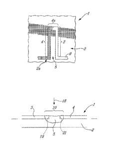
Turning to Figure 7, arrow 18 depicts the direction of application of a
focused
heating source pulse onto the semiconductor device 1, As may be understood, a
focused heating source may be disposed (not shown) above the integrated
semiconductor device 1, and which may apply a pulse 18 to the device 1 As may
be
understood, the dimensions of the pulse 18 and of the device 1 may not be to
scale.
Figure 7, also shows, in enlarged fashion, a cross sectional view of the
tunable
integrated semiconductor device 1 through the solidified bridge 10 as shown in
Figure
5. The solidified bridge 10 was obtained by the application of a focused
heating pulse
18 to a pre-selected or pre-determined area comprising a portion of lightly
doped gap
region 5, as well as adjacent portions 19 and 21 of heavily doped link
portions 3 and 4
respectively (shown in dotted lines), so as to melt the affected areas and
obtain a
melted pool (eventually solidifying into bridge 10. As may be appreciated, a
portion of
heavily doped link portions 3 and 4 is included in the melted pool. The extent
of heavily
doped regions 3 and 4 which will melt subsequent to the application of the
heating pulse
18 may depend on the characteristics of the heating pulse, namely the power of
the
pulse, the duraticn of the application of the pulse, the diameter of the
pulse, etc...: the
diameter of the heating pulse may for example be such as to span a portion of
the gap
region and encompass a portion of both of heavily doped link portions 3 and 4.
The
longer melted pool is melted, the greater the diffusion of dopant from heavily
doped
CA 02436759 2013-03-06
27
regions 3 and 4 into lightly doped region 5. However, the amount of dopants
which wilt
diffuse from heavily doped portions 3 and 4 into lightly doped gap region 5
may also
depend on how much of heavily doped regions 3 and 4 may be caught by the
focused
heating beam 18, i.e. if a large part of heavily doped regions 3 and/or 4 are
caused to
be melted, more dopants may diffuse, and if a small part is caused to be
melted, fewer
dopants may diffuse. Depending on the length of time that the melted pool
remaines
melted, the dop ant profile across the melted pool from heavily doped region 3
to heavily
doped region 4 may not be uniform. Although it is advantageous to form a
conductive
bridge between link portions 3 and 4 by use of a single heating pulse spanning
the gap
region 5, it may if so desired be possible to use a plurality of smaller
diameter heating
pulses. If a plurality of heating pulses are applied they may be applied in
stepwise
fashion starting for example from an initial step comprising melting a portion
of one link
portion and an adjacent portion of the gap region 5 and then proceeding in
stepwise
fashion across the gap region 5 to finally melt a portion of the other link
portion and an
adjacent portion of the gap region 5.
Turning to Figures 9a, 9b arid 9c, these figures Illustrate a number of
enlarged
example (laser) pulse target areas which are derived from a preselected bridge
area for
the device as shown in figures Ito 5; for illustration purposes the bridge
area boundary
and the target area boundaries for figures 9b and 9c are shown as not being
contiguous;
for actual applications, after a bridge cycle the boundaries of the bridge
area and related
target area(s) will be contiguous. The bridge area in each case has a border
which is
designated by the reference numeral 20. The bridge area as may be seen has a
gap
component 22 , a first link component 24 and a second link component 26; each
of these
component respectively comprises a portion of gap region 5, first link member
3 and
second link member 4. Figure 9a illustrates a single target area wherein the
boundary
of the target area is the same as that of the bridge area itself. Figure 9b
illustrates a
pair of target areas which, for illustration purposes only, are within the
bridge area
boundary and have boundaries 30 and 32 which overlap in the gap component.
Figure
9c shows three target areas which, for illustration purposes only, are also
within the
bridge area boundary and have boundaries 34, 36 and 38 which overlap in the
gap
CA 02436759 2013-03-06
28
component. The target area 36 is subject to the heat/cooling treatment after
at least one
of the other target areas has been so subjected so as to draw dopant from the
treated
area(s).
Turning back to Figures 8 and 9 there is illustrated a representation of a
general
embodiment of an apparatus 100 for modifying the impedance of an Integrated
semiconductor device using a focused heating source, such as a laser. An
integrated
circuit 110 Is placed on a positioning table 10, and may be subjected to en
application
of a heating source 105 which is produced by a focused heating source 103.
Heating
source 105 may be focused on integrated circuit 110 by using optic or magnetic
lenses
107, and a system of cameras and mirrors allows for the observation of the
integrated
circuit 110 in order to ensure accurate alignment of the heating source 105.
Figure 12
shows apparatus 100 in greater detail. Laser 103 is connected to shutter 118,
each of
which is controlled by the control system shown as a computer 408. Also
connected to
computer 108 is the control mechanism 109 of the positioners 101. The
apparatus 100
further comprises a camera 112, and a light source 114. A further component of
the
apparatus 100 is a beam splitter 113. and a selective mirror 120.
Turning to Figures 10 to 13, these figures illustrate examples of possible
applications of the present invention
FIG. 10 illustrates an example electric schematic of an example series
resistor
ladder for an analogue to digital converter which provided with a number of
resistance
members each generally designated as R. FIG 11 illustrates how the series
resistor
ladder of Fig 10 may be formed using a plurality of integrated semiconductor
devices
as shown in Figure 5; i.e. each device of rig. 5 may be disposed so as to each
define
a respective resistance or impedance member of the analogue to digital
converter of
example 10, one of the devices, as shown in Figure 6, and which defines a
resistance
R is shown as being designated by the reference numeral 130 in Figure 11. Once
the
general structure of Fig 11 is formed by conventional techniques (i.e. laying
down of
CA 02436759 2013-03-06
29
appropriately doped layers, substrates and regions, etc.) fine tuning of each
of the
members 130 may be carried out as described herein.
PG. 12 illustrates an example electric schematic of an R-2R resistor ladder
for
a digital to analogue converter provided with a number of resistance members
each
generally designated either as R or 2R; FIG. 13 illustrates how a plurality of
integrated
semiconductor devices as shown in Figure 5 may be disposed so as to define the
analogue to digital converter of example 12. Reference numerals 140 and 150
generally designate devices of figure 5 which define respectively a resistance
R or 2R.
Once the general structure of Fig 13 is formed by conventional techniques
(i.e. laying
down of appropriately doped layers, substrates and regions, etc.) fine tuning
of each of
the members 140 and 150 may be carried out as described herein.
FIG. 14 illustrates an example of another tunable integrated semiconductor
device
of the present Invention wherein one of the link portions of the crimp or fold
element is
not (initially) In the main conductive path. The device 154 comprises various
layers or
regions, for example, a non-conductive substrate 156, and a conductive layer
or region
158 which is contiguous with the underlying substrate 156. In this case, the
conductive
layer or region 158 comprises a gross, major or large link member or portion
160 and
a minor link member or portion 161. The large link portion 160 corresponds to
the first
conductive link portion which defines the base conductive path of the device:
thus the
major or large link portion 160, itself alone initially forms the main
conductive path
between contact members 162 and 164, i.e. current is at least initially able
to pass
through the entire region 158 between these contact members 162 and 164. The
minor
link portion 161 which is electrically connected at one end thereof to the
major link
portion by connector member 168, is spaced apart from the link portion 160 by
a gap
region 170 which is part of the substrate 156. The impedance (Le resistance)
of the
device of Fig. 14 is modified (i.e lowered) by providing conductive bridges
across the
gap region 170 as described above with respect to the device of Fig. 5. The
creation
of the conductive bridges across the gap region 170 will modify the effective
(electrical)
dimension of the device so as to slightly change the overall resistance of the
device 154.
CA 02436759 2013-03-06
This gap/fink configuration may be used to provide a more precise tuning of
the
resistance of a device than by the devices shown in Fig.1 to 5.
FIG. 15 illustrates an example combination of an integrated semiconductor
5 device as shown in Figure 5 with an integrated semiconductor device as
shown in Figure
14 to provide a device which may be tuned with higher precision than would be
obtainable by the device of FIG. 5 alone. For this overall device initial
tuning of the
structure of Fig 5 may give a precision of for example 0.01% whereas tuning of
the
structure of Fig 14 may give an overall precision for the device of 0.001%.
The device or component of Figure 15 also has contact or connecter members
8 and 174 for electrically connecting the conduction region(s) to other
devices, current
is at least initially able to pass through the entire region(s) a between
these contact
members.
Referring to figures 16, the same reference numerals as used in figures Ito 5
to
denote common or analogous elements will be used with respect to this figure
as well.
The device 1 of FIG. 16 as in the case of the devices of figures 1 to 5 has a
non-
conductive substrate 2, and a sinuous conductive layer or region 2a which is
contiguous
with the underlying substrate 2. The conductive region 2a is disposed in the
form of a
conductive crimp element similar to that as set out in Fig 1 but wherein the
top half
portion is bent over downwardly. As may be seen, the top portion is bent over
downwardly so as to provide the device 1 with an outer U shaped member and an
inner
U shaped member. The inner U shape member is nested in the outer U shaped
member so as to provide the device 1 with a first gap region 5 and a second
inner gap
region 5a, The first gap region 5 spaces apart the two U shaped members such
that the
outer U shaped member may be considered to be a first link member as described
herein and the inner U shaped member to be a second link member also as
described
herein. On the other hand, the second inner gap region 5a, also spaces apart
portions
of the inner U shaped member in a manner reminiscent of the first and second
link
members as shown in figure 1. As a result, the device of figure 16 may not
only provide
CA 02436759 2013-03-06
31
for one or more outer conductive bridges such as for example conductive
bridges 200
and 202 but also one or more inner conductive bridges such as for example
inner
conductive bridge 204.
Turning to figure 17, this Figure illustrates a electrical schematic of the
device
shown in Figure 16 tuned only with the above mentioned bridges 200, 202 and
204.
The reference numeral 210 designates the base or main initial impedance (i.e.
resistance) represented by region 2a as a whole The reference numerals 212.214
and
216 represent respective secondary resistances defined by bridges 200. 202 and
204
respectively