Note: Descriptions are shown in the official language in which they were submitted.
CA 02436898 2003-08-08
TITLE OF THE INVENTION
CARTRIDGE AND RECORDING APPARATUS
BACKGROUND OF THE INVENTION
Field of the Invention
[0001]
The present invention relates to a cartridge that has a chamber
for holding a recording material used for recording therein. More
specifically the invention pertains to a cartridge with a built-in
non-volatile memory and a technique of transmitting information
to and from such a cartridge.
Description of the Related Art
[0002]
Recording apparatus that ej ect inks on printing paper to record
images, such as ink jet printers, and recording apparatus that
utilize toners for recording have widely been used. A cartridge
attached to such a recording apparatus has a chamber for holding
a recording material like ink or toner therein. Management of the
residual quantity of the recording material is an important
technique in the recording apparatus. The recording apparatus
counts the consumption of the recording material according to the
software program. Data on the residual quantity of the recording
material computed from the observed count are stored in a memory
of the recording apparatus for the management purpose . The same
data may also be stored in a built-in memory of the cartridge.
[0003]
1
CA 02436898 2003-08-08
A non-volatile memory is applicable for the built-in memory
of the cartridge . The non-volatile memory enables data, such as
the residual quantity of ink, to be kept even after detachment
of the cartridge from the recording apparatus . Application of such
a memory ensures consistent management of the residual quantity
of ink and other data even when the replaced cartridge is attached
again to the recording apparatus.
[0004]
An important issue of such cartridges with the built-in memory
is to ensure a sufficiently high reliability in the storage content
of the memory. There are two primary causes of lowering the
reliability in the storage content of the memory. One cause is
an accidental cutoff of the power supply to the recording apparatus
in the course of updating data into the cartridge or a careless
detachment of the cartridge in the course of updating data. In
such cases, it is practically impossible to verify the updated
storage content in the memory of the cartridge . The other cause
is a failed electrical connection. The cartridge is basically
des igned to be freely attachable to and detachable from the recording
apparatuso that no fixed signal line is usable for connection with
the memory in the cartridge. This may cause a loose contact or
another failure in electrical connection.
[0005]
One possible measure carries out the memory updating operation
a plurality of times. Another possible measure providesduplicate
memories and writes identical data into the duplicate memories.
In the case of a loose connection of a signal line, however, these
CA 02436898 2003-08-08
measures do not heighten the reliability. When an electrically
erasable semiconductor memory (EEPROM) is applied for the built-in
memory of the cartridge, the data rewriting procedure first erases
the existing data in the memory and then new data into the memory.
This requires two normal accesses for easing and writing data and
thus demands a high reliability.
SUi~ARY OF THE INVENTION
(ooo6J
The object of the present invention is thus to remove the
drawbacks of the prior art techniques and to ensure a sufficiently
high reliability in the operation of updating data in a cartridge
equipped with a memory.
[0007)
In order to attain at least part of the above and the other
related obj ects , the present invention is directed to a cartridge
that holds a recording material used for recording therein and
is mounted on a recording apparatus. The cartridge includes: a
memory that stores information regarding the cartridge in a
non-volatile manner; aninstruction reception modulethat receives
an external instruction including at least a specified address
of the memory with regard to a series of processing that involves
rewriting a storage content of the memory; a processing execution
module that executes the series of processing that involves
rewriting the storage content at the specified address of the memory;
and an output module that outputs specific data corresponding to
the specified address after execution of the series of processing.
3
CA 02436898 2003-08-08
[0008]
The cartridge has the memory that stores the cartridge-related
information in a non-volatile manner and receives an external
instruction including at least a specified address of the memory
with regard to a series of processing that involves rewriting the
storage content of the memory. The cartridge executes the series
of processing that involves rewriting the storage content at the
specified address of the memory in response to the given external
instruction, and outputs specific data corresponding to the
specified address. The specific data corresponding to the
specified address may be identical with the specified address or
data representing multiple upper bits or multiple lower bits of
the specified address. The specific data may otherwise be a
checksum of the specified address, a cyclic redundancy code (CRC) ,
or a hamming code. The recording apparatus, which has given the
external instruction with regard to the series of processing that
involves rewriting the storage content of the memory, reads the
output data and verifies whether the series of processing has been
executed successfully at the specified address.
[0009]
The series of processing that involves rewriting the storage
content of the memory may be an operation of writing data into
the memory or an operation of erasing data from the memory. In
some memories, the data erasing operation is required prior to
the data writing operation. In such cases, the series of processing
includes the data erasing operation and the subsequent data writing
operation.
CA 02436898 2003-08-08
[0010]
when the series of processing that involves rewriting the
storage content of the memory is the data erasing operation, it
is preferable that the externally specified address with regard
to the data erasing operation has a redundancy of at least 2. The
data erasing operation eliminates the storage content of the memory,
so that the high redundancy of the specified address, for example,
duplication of the address, is desirable. For example, the
redundancy of at least 2 possessed by the specified address is
attained by a signal corresponding to the specified address and
a signal generated by changing bits of the specified address
according to a preset rule . Here the preset rule may be at least
one of a reciprocal operation, a complementary operation, and a
bit rotation.
[0011]
The data output by the output module in response to the
externally specified address may be any data corresponding to the
specified address; for example, data identical with the specified
address, data representing a predetermined part of the specified
address, or a code induced from the specified address like a parity
code, a hamming code, or a CRC. These codes desirably reduce the
number of bits included in the output data, compared with the number
of bits constituting the specified address.
[0012]
The output module may output the specific data together with
a signal representing completion of the series of processing, after
conclusion of the series of processing that involves rewriting
5
CA 02436898 2003-08-08
the storage content of the memory. The specific data may otherwise
be output separately from the signal representing completion of
the series of processing. The simultaneous output desirably
shortens the total processing time, whereas the separate output
desirably enhances the degree of freedom in data structure.
[0013]
The data rewritten in the memory may be data regarding a residual
quantity or a consumption of the recording material held in the
cartridge, data relating to a state of the processing, data regarding
occurrence of any abnormality, data regarding the frequency of
detachment of the cartridge or accumulation of the use time of
the cartridge, or data regarding the working environment, for
example, the temperature and the humidity.
[0014)
The recording material held in the cartridge may be a preset
color ink used for a printer or another recording apparatus or
a toner for a photocopier, a facsimile, or a laser printer. The
recording material may be any material that allows for recording
in any manner, for example, a material for a semiconductor or a
solution of a catalyst.
[0015)
The memory may be a general parallel access-type memory, but
a serial access-type memory is also applicable to reduce the number
of signal lines required for signal transmission. The memory
desirably has non-volatility or is backed up by a battery.
Preferable examples are an electrically erasable programmable
memory (EEPROM) and a dielectric memory.
6
CA 02436898 2003-08-08
[0016]
Data may be transmitted to and from the cartridge by wire
communication or by wireless communication. The technique of
partial wire communication and partial wireless communication is
also applicable. In the case of wireless communication, the
cartridge further includes a wireless communication module that
transmits data to and from an outside by wireless communication.
At least one of the instruction with regard to the series of
processing that involves rewriting the storage content of the memory,
the specified address, and the specific data corresponding to the
specified address is transmitted via the wireless communication
module. The wirelesscommunication doesnotrequire any additional
electrical connection means like a connector or a terminal and
thus facilitates attachment and detachment of the cartridge.
[0017]
In one preferable embodiment, the wireless communication
module has a loop antenna that is used to establish the communication,
and a power supply module that utilizes an electromotive force
induced in the antenna to supply electric power to the cartridge .
This structure does not require any additional power source, for
example, a battery, in the cartridge for wireless communication.
The cartridge mayotherwise include aprimarybattery, ora secondary
battery or a capacitor in addition to or in place of the primary
battery.
[0018]
The present invention is also directed to a recording apparatus,
on which a cartridge having a chamber f or holding a recording material
CA 02436898 2003-08-08
used for recording therein is mounted. The cartridge includes:
a memory that stores information regarding the cartridge in a
non-volatile manner;aninstruction reception modulethat receives
an external instruction including at least a specified address
of the memory with regard to a series of processing that involves
rewriting a storage content of the memory; a processing execution
module that executes the series of processing that involves
rewriting the storage content at the specified address of the memory;
and an output module that outputs specific data corresponding to
the specified address after execution of the series of processing.
The recording apparatus includes: an address specification
module that specifies the address at which the storage content
of the memory is to be rewritten; an input module that inputs the
specific data corresponding to the specified address output from
the output module of the cartridge; and a verification module that
compares the input specific data with the address specified by
the address specification module and, when the input specific data
is identical with the specified address, verifies that the series
of processing that involves rewriting the storage content of the
memory has been implemented normally.
[0019]
The recording apparatus of the invention gives an instruction
including a specified address with regard to a series of processing
that involves rewriting the storage content of the memory included
in the cartridge . The cartridge executes the series of processing
that involves rewriting the storage content at the specified address
of the memory in response to the given instruction, and outputs
8
CA 02436898 2003-08-08
at least the specific data corresponding to the specified address
to the recording apparatus. The recording apparatus reads the
output specific data and compares the specific data with the
specified address. When the specific data is identical with the
specified address, the recording apparatus verifies that the series
of processing that involves rewriting the storage content at the
specified address of the memory has been implemented normally.
This arrangement verifies whether data has been rewritten
successfully at a right address and thus enhances the reliability
in the storage content of the memory in the cartridge.
foo2o]
In one preferable arrangement of the invention, the recording
apparatus compares the specific data with the address specified
by the address specification module and, when the specific data
is different from the specified address, causes the processing
executionmodule of the cartridge to execute the series of processing
that involves rewriting the storage content of the memory all over
again and thereby correct a mistake. This further enhances the
reliability in the storage content of the memory. Another
preferable arrangement gives a notification representing the
discrepancy, when the specific data is different from the specified
address . This arrangement informs the user of the occurrence of
some error and thereby enhances the reliability of the recording
apparatus and the cartridge. In one preferable embodiment, the
address specification module of the recording apparatuspecifies
the address by a signal representing the address at which the storage
content of the memory is to be rewritten and a signal generated
9
CA 02436898 2003-08-08
by changing bits of the address according to a preset rule . Here
the preset rule may be at least one of a reciprocal operation,
a complementary operation, and a bit rotation.
[0021]
The technique of the present invention is not restricted to
the cartridge or the recording apparatus of various arrangements
discussed above, but is also applicable to an information
transmitting method.
[0022]
The present invention is thus directed to a method of
transmitting information to and froma cartridge, which has a chamber
for holding a recording material used for recording therein. The
information transmitting method includes the steps of : giving an
external instruction including at least a specified address with
regard to a series of processing that involves rewriting a storage
content of a memory from an outside of the cartridge, the memory
being provided in the cartridge to store information regarding
the cartridge in a non-volatile manner; ~~~J- causing the cartridge
to execute the series of processing that involves rewriting the
storage content at the specified address of the memory and outputting
specific data corresponding to the specified address to the outside
of the cartridge; and comparing the output specific data with the
specified address and verifying whether the series of processing
that involves rewriting the storage content of the memory has been
implemented normally.
[0023]
These and other objects, features, aspects, and advantages
CA 02436898 2003-08-08
of the present invent ion will become more apparent from the following
detailed description of the preferred embodiment with the
accompanying drawings.
[0024]
BRIEF DESCRIPTION OF THE DRAWINGS
Fig. 1 schematically illustrates the structure of an ink
cartridge and a printer, to which the ink cartridge is attached,
in one mode of the invention;
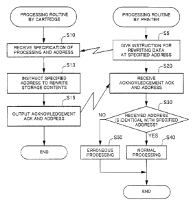
Fig. 2 is a flowchart showing a series of processing executed
by a memory controller of the ink cartridge, in combination with
a series of processing executed by a control unit of the printer;
Fig. 3 schematically illustrates the structure of an ink jet
printer in one embodiment of the invention;
Fig. 4 shows the electric construction of a control circuit
included in the printer of the embodiment;
Figs. 5A and 5B show the appearance of a detection memory
module in the embodiment;
Fig. 6 is an end view showing attachment of the detection
memory module to an ink cartridge in the embodiment;
Fig. 7 is a block diagram showing the internal structure of
the detection memory module;
Figs . 8A and 8B show the positional relation between a receiver
transmitter unit and ink cartridges mounted on a carriage of the
printer;
Figs. 9A and 9B show information stored in an EEPROM as an
internal memory of the detection memory module;
11
CA 02436898 2003-08-08
Fig. 10 is a flowchart showing a series of processing executed
by the control circuit of the printer in cooperation with the
detection memory module attached to each ink cartridge;
Fig. 11 is a timing chart in a data rewriting operation in
the EEPROM; and
Fig. 12 is a flowchart showing a verification routine executed
by the control circuit of the printer in the data rewriting operation
in the EEPROM.
DESCRIPTION OF THE PREFERRED EMBODIMENTS
[0025]
Fig. 1 schematically illustrates the structure of an ink
cartridge 10 and a printer 20 as a recording apparatus, to which
the ink cartridge 10 is attached, in one mode of the invention.
The printer 20 makes ink ejected from a print head 25 and thereby
prints an image on printing paper T, which is transported by means
of a platen 24 . The printer 20 includes a control unit 22, although
the internal structure of the printer 20 is not described nor
illustrated specifically. The control unit 22 computes an ink
consumption used for printing and other required data and transmits
the computed data to the ink cartridge 10 via a receiver transmitter
unit 30. Data are transmitted between the printer 20 and the ink
cartridge l0 bywireless, although wire communicationmaybe adopted
alternatively. The electromagnetic induction technique is
applied for wireless communication in this mode of the invention,
though another technique is also applicable.
[0026]
12
CA 02436898 2003-08-08
The ink cartridge 10 includes a communication controller 12
that controls communication, a memory controller 15 that controls
reading and writing data from and into a memory 14, a sensor 17
of a piezoelectric element , and a sensor controller 19 that actuates
and controls the sensor 17 to detect a residual level of ink. The
memory controller 15 transmits data to and from the memory 14,
in response to instructions output from the printer 20 and received
by the communication controllerl2. The datatransmissionincludes
three primary processes, that is, a process of reading data from
a specified address in the memory 14, a process of erasing data
f rom the specified address in the memory 14 , and a process of writing
data at the specified address in the memory 14. The sensor
controller 19 actuates the sensor 17 and detects the residual level
of ink by taking advantage of a variation in resonance frequency
of a resonance chamber 18 provided in an ink chamber 16.
[0027]
Fig . 2 is a flowchart showing a series of processing executed
by the memory controller 15, in combination with a series of
processing executed by the control unit 22 of the printer 20. The
memory controller 15 is actualized, for example, by a circuit
structure including a gate array. For convenience of the
explanation, however, the respective operations performed in the
memory controller 15 are described according to the flowchart.
The control unit 22 of the printer 20 gives an instruction for
rewriting the storage contents at a specific address in the memory
14 (step S5) . More specifically, the control unit 22 gives either
an instruction for erasing data from the specified address in the
13
CA 02436898 2003-08-08
memory 14 or an instruction for rewriting data at the specified
address in the memory 14. The memory controller 15 of the ink
cartridge 10 receives the given instruction including the
specification of the required processing and the specified address
as the object to be processed (step S10).
[0028]
The memory controller 15 then instructs the specified address
in the memory 14 to rewrite its storage contents (step S13) . The
concrete procedure of this step outputs a 1-byte operand and a
1-byte address to the memory 14. The 1-byte operand represents
the specification of the required processing, for example, an
erasing operation, a reading operation, or a writing operation.
The address is specified by the 1-byte data in this description,
but the data size may be varied according to the length of the
address in the case of the memory 14 having a sufficiently large
storage capacity. For the enhanced reliability, even if the
capacity of 1 byte is enough for the data size of the address,
the capacity of 2 bytes may be assigned to the address specif ication.
For example, an identical address is output consecutively as the
2-byte data after the 1-byte operand representing either a rewriting
or erasing operation. In another example, 1-byte complement
address data may follow the 1-byte address specification data.
The order of the latter 2-byte data may be inverted. Namely the
instruction may include the 1-byte operand representing either
a rewriting operation or an erasing operation, the 1-byte complement
address data, and the 1-byte address data in this order. The 1-byte
data added to the address may be obtained by a preset arithmetic
14
CA 02436898 2003-08-08
operation, for example, a reciprocal operation, a complementary
operation, or a bit rotation, of the bit sequence representing
the address . The additional 1-byte data is not restricted to the
arithmetic operation of the address, but may be a checksum of the
address, a hamming code, an error correcting code, or any other
suitable data.
[0029]
The memory 14 receives the operand and the address output
from the memory controller 14, rewrites or erases data at the
specified address in response to the given instruction, and sends
back a signal representing a concluded access to the memory
controller 15 within a preset time . The memory controller 15 is
accordingly informed of the result of the data rewriting or erasing
operation at the specified address in the memory 14. The memory
controller 15 then outputs an acknowledgement ACK and the 1-byte
address as the object of the data rewriting operation via the
communication controller 12 (step S15).
(0030]
The control unit 22 of the printer 20 receives the
acknowledgement ACK and the address as the object of the data
rewriting operation (step S20) and compares the received address
with the address specified previously by the control unit 22 (step
S30). When the address received from the ink cartridge 10 is
identical with the address specified previously by the control
unit 22 , the control unit 22 determines that data has been rewritten
normally ( step S40 ) . When the received address is not identical
with the specified address, on the other hand, the control unit
CA 02436898 2003-08-08
22 determines that there has been some error in the process of
rewriting data at the specified address in the memory 14 of the
ink cartridge 10 (step S50).
[0031]
As described above, the technique of the invention applied
to the ink cartridge 10 enables the storage contents to be rewritten
at an externally specified address in the memory 14 and allows
the specified address as the object of rewriting to be checked
after the data rewriting operation. Even if the specified address
in the memory 14 is changed by noise or another reason, this
arrangement effectively informs the control unit 22 of the printer
of an erroneous data rewriting operation at a wrong address.
[0032]
This technique of the invention is applicable to various
15 printers. The following describes application of the invention
to an ink jet printer 200 as one embodiment. Fig. 3 schematically
illustrates the structure, especially the operation-related
structure, of the ink jet printer 200. Fig. 4 shows the electric
construction of a control circuit 222 of the printer 200 . As shown
20 in Fig. 3, the printer 200 makes ink droplets ejected from print
heads 211 through 216 onto printing paper T, which is fed from
a paper feed unit 203 and is transported by means of a platen 225,
so as to form an image on the printing paper T. The platen 225
is actuated and rotated by the driving force transmitted from a
paper feed motor 240 via a gear train 241. The rotational angle
of the platen 225 is measured by an encoder 242. The print heads
211 through 216 are mounted on a carriage 210, which moves back
16
CA 02436898 2003-08-08
and forth along the width of the printing paper T. The carriage
210 is linked with a conveyor belt 221, which is actuated by a
stepping motor 223. The conveyor belt 221 is an endless belt and
is spanned between the stepping motor 223 and a pulley 229 arranged
on the opposite side . With rotations of the stepping motor 223 ,
the conveyor belt 221 moves to reciprocate the carriage 210 along
a conveyor guide 224.
(0033]
Ink cartridges 111 through 116 of six different color inks
are attached to the carriage 210. The six color ink cartridges
111 through 116 basically have an identical structure and
respectively store inks of different compositions, that is, inks
of different colors, in their internal ink chambers. More
specifically, the ink cartridges 111 through 116 respectively store
black ink (K) , cyan ink (C) , magenta ink (M) , yellow ink (Y) , light
cyan ink ( LC ) , and 1 fight magenta ink ( LM ) . The 1 fight cyan ink ( LC )
and the light magenta ink (LM) are regulated to have 1/4 of the
dye densities of the cyan ink (C) and the magenta ink (M) . Detection
memory modules 121 through 126 (discussed later) are attached to
these ink cartridges 111 through 116, respectively. The detection
memory modules 121 through 126 transmit data to and from the control
circuit 222 of the printer 200 by wireless communication. In the
structure of this embodiment, the detection memory modules 121
through 126 are attached to the respective side planes of the ink
cartridges 111 through 116.
(0034]
The printer 200 has a receiver transmitter unit 230 to establish
1i
CA 02436898 2003-08-08
wireless communication with and data transmission to and from these
detection memory modules121through126. The receivertransmitter
unit 230, as well as the paper feed motor 240, the stepping motor
223, the encoder 242, and the other electronic parts, are connected
to the control circuit 222. Diverse switches 247 and LEDs 248 on
an operation panel 245 located on the front face of the printer
200 are also connected with the control circuit 222.
[0035]
As shown in Fig. 4, the control circuit 222 includes a CPU
251 that controls the constituents of the whole printer 200, a
ROM 252 that stores control programs therein, a RAM 253 that is
used to temporarily register data, a PIO 254 that functions as
an interface with external devices, a timer 255 that manages the
time, and a drive buffer 256 that stores data for driving the print
heads 211 through 216. These circuit elements are mutually
connected via a bus 257. The control circuit 222 also includes
an oscillator 258 and an output divider 259, in addition to these
circuit elements . The output divider 259 distributes a pulse signal
output from the oscillator 258 into common terminals of the six
print heads 211 through 216. Each of the print heads 211 through
216 receives dot on-off data (ink ejection non-ejection data) from
the drive buffer 256 and makes the ink ejected from corresponding
nozzles according to the dot on-off data received from the drive
buffer 256 in response to driving pulses output from the output
divider 259.
[0036]
A computer PC that outputs object image data to be printed
18
CA 02436898 2003-08-08
to the printer 200, as well as the stepping motor 223, the paper
feed motor 240, the encoder 242, the receiver transmitter unit
230, and the operation panel 245 are connected to the PIO 254 of
the control circuit 222 . The computer PC specifies an obj ect image
to be printed, makes the specified obj ect image subj ected to required
series of processing, such as rasterizing, color conversion, and
halftoning, and outputs resulting processed data to the printer
200. The printer 200 detects the moving position of the carriage
210 according to the driving quantity of the stepping motor 223 ,
while checking the paper feed position based on the data from the
encoder 242. The printer 200 expands the processed data output
from the computer PC into dot on-off data representing ink ejection
or non-ejection from nozzles of the print heads 211 through 216
and actuates the drive buffer 256 and the output divider 259.
[0037]
The control circuit 222 transmits data by wireless to and
from the detection memory modules 121 through 126 attached to the
ink cartridges 111 through 116 via the receiver transmitter unit
230 connecting with the PIO 254. The receiver transmitter unit
230 accordingly has an RF conversion element 231 that converts
signals from the PIO 254 into alternating current (AC) signals
of a fixed frequency, and a loop antenna 233 that receives the
AC signals from the RF conversion element 231 . When the loop antenna
233 receives the AC signal, the electromagnetic induction excites
an electric signal in another antenna located close to the loop
antenna233. The distance of wireless communicationis restricted
in the printer 200, so that electromagnetic induction-based
19
CA 02436898 2003-08-08
wireless communication technique is adopted in the structure of
this embodiment.
[0038]
The following describes the structure of the detection memory
module 121 attached to the ink cartridge 111. Figs . 5A and 5B are
a front view and a side view showing the detection memory module
121. The detection memory modules 121 through 126 mounted on the
respective ink cartridges 111 through 116 have an identical
structure, except ID numbers stored therein. The discussion
accordingly regards the detection memory module 121 as an example .
As illustrated, the detection memory module 121 has an antenna
133 formed as a metal thin film pattern on a thin film substrate
131, an exclusive IC chip 135 having diverse functions built therein
as discussed later, a sensor module 137 that detects the presence
or the absence of ink, and a wiring pattern 13 9 that mutually connects
these constituents.
[0039]
Fig. 6 is an end view showing attachment of the detection
memory module 121 to the ink cartridge 111. The detection memory
module 121 is fixed to the side face of the ink cartridge 111 by
means of an adhesive layer 141 of, for example, an adhesive or
a double-faced tape. The sensor module 137 disposed on the rear
face of the substrate 131 is f it in an opening formed in the side
plane of the ink cartridge 111. A resonance chamber 151 is formed
inside the sensor module 137, and a piezoelectric element 153
functioning as a sensor is bonded to the side wall of the resonance
chamber 151.
CA 02436898 2003-08-08
[0040]
Fig . 7 is a block diagram showing the internal structure of
the detection memory module 121. The detection memory module 121
has an RF circuit 161, a power supply unit 162, a data analyzer
163 , an EEPROM controller 165 , an EEPROM 166, a detection controller
168 that transmits data to and from the sensor module 137 equipped
with the piezoelectric element 153 to detect the residual quantity
of ink, and an output unit 178, which are all built in the exclusive
IC chip 135.
[0041]
The RF circuit 161 demodulates an AC signal generated in the
antenna 133 by the electromagnetic induction, extracts an electric
power component and a signal component from the demodulated AC
signal, and outputs the electric power component to the power supply
unit 162 while outputting the signal component to the data analyzer
163. The RF circuit 161 also functions to receive a signal from
the output unit 178 (described later) , modulates the received signal
to an AC signal, and transmits the modulated AC signal to the receiver
transmitter unit 230 of the printer 200 via the antenna 133. The
power supply unit 162 receives the electric power component from
the RF circuit 161, stabilizes the received electric power component,
and outputs the stabilized electric power component as power sources
of the exclusive IC chip 135 and the sensor module 137. No
independent power source, such as dry cells, is thus required for
each of the ink cartridges 111 through 116 . When the signal-induced
power supply time from the receiver transmitter unit 230 is
restricted, the detection memory module 121 may additionally have
21
CA 02436898 2003-08-08
a charge accumulator element, such as a capacitor, that effectively
accumulates the stabilized power source generated by the power
supply unit 162. The charge accumulator element may be disposed
before the power supply unit 162.
[0042]
The data analyzer 163 analyzes the signal component received
from the RF circuit 161 and extracts a command and data from the
analyzed signal component . The data analyzer 163 specifies either
data transmission to and from the EEPROM 166 or data transmission
to and from the sensor module 137, based on the result of the data
analysis. The data analyzer 163 also carries out identification
of the object ink cartridge of the data transmission to and from
either the EEPROM 166 or the sensor module 137. The details of
the identification process will be discussed later, but basically
the identification process identifies the ink cartridge, based
on information representing the location of each ink cartridge
mounted on the carriage 210 relative to the receiver transmitter
unit 230 as shown in Figs. 8A and 8B and the ID stored in each
ink cartridge . Fig. 8A is a perspective view showing the positional
relation between the ink cartridges 111 through 116 with the
detection memory modules 121 through 126 attached thereto and the
receiver transmitter unit 230. Fig. 8B shows the relative widths
of the ink cartridges 111 through 116 and the receiver transmitter
unit 230.
(0043]
For identification of the object ink cartridge, the control
circuit 222 shifts the carriage 210 to approach to the receiver
CA 02436898 2003-08-08
transmitter unit 230. The location of the carriage 210 facing the
receiver transmitter unit 230 is outside a printable range. As
shown in Figs . 8A and 8B, the detection memory modules 121 through
126 are attached to the side faces of the respective ink cartridges
111 through 116 . The shift of the carriage 210 causes two detection
memory modules at the maximum to enter a transmittable range of
the receiver transmitter unit 230 . In this state, the data analyzer
163 receives a request from the control circuit 222 via the receiver
transmitter unit 230 and performs identification of the object
ink cartridge and subsequent data transmission to and from the
EEPROM 166 or the sensor module 137. The details of the processing
will be discussed later with reference to the flowchart.
[0044]
When data transmission to and from the EEPROM 166 is performed
after identification of the object ink cartridge, the data analyzer
163 transfers a specified address for a reading, writing, or erasing
operation and specification of the processing, that is, selection
of the reading operation, the writing operation, or the erasing
operation, as well as data in the case of the data writing operation,
to the EEPROM controller 165. The EEPROM controller 165 receives
the specified address, the specification of the processing, and
the data to be written and outputs the specified address and the
specification of the processing to the EEPROM 166, so as to read
the existing data from the specified address of the EEPROM 166,
write the received data at the specified address of the EEPROM
166, or erase the existing data from the specified address of the
EEPROM 166.
23
CA 02436898 2003-08-08
[0045]
The internal data structure of the EEPROM 166 is shown in
Figs. 9A and 9B. The memory space of the EEPROM 166 is roughly
divided into two sections as shown in Fig. 9A. The former section
of the memory space is a readable and writable area RAA including
a classification code area and a user memory area, which data like
the residual quantity of ink are read from and written in. The
latter section of the memory space is a read only area ROA which
ID information for identifying the ink cartridge is written in.
[0046]
The ID information is written into the read only area ROA
prior attachment of each of the detection memory modules 121 through
126 including the EEPROM 166 to the corresponding ink cartridge
111 through 116, for example, in the manufacturing process of the
detection memory module or in the manufacturing process of the
ink cartridge . The printer 200 is allowed to write data into the
readable writable area RAA and read and erase the existing data
stored in the readable writable area RAA. The printer 200 is,
however, not allowed to write data into the read only area ROA,
while being allowed to read data from the read only area ROA.
[004]
The user memory area of the readable writable area RAA is
used to write information regarding the residual quantity of ink
in the corresponding ink cartridge 111 through 116. The printer
200 reads the information on the residual quantity of ink and may
give an alarm to the user when the residual quantity of ink is
below a preset level. The classification code area stores various
24
CA 02436898 2003-08-08
codes for distinction of the corresponding ink cartridge . The user
may use these codes according to the requirements.
[0048]
The ID information stored in the read only area ROA includes
productioninformation onthe correspondingink cartridge,to which
the detection memory module is attached. A typical example of the
ID information regards the year, the month, the date, the hour,
the minute, the second, and the place of production of the
corresponding ink cartridge 111 through 116 as shown in Fig . 9B .
Each piece of the ID information requires a memory area of 4 to
8 bits, so that the ID information totally occupies a memory area
of 40 to 70 bits. On each power supply of the printer 200, the
control circuit 222 of the printer 200 may read the ID information
including the production information of the ink cartridges 111
through 116 from the detection memory modules 121 through 126 and
give an alarm to the user when any of the ink cartridges has been
expired or will be expired soon.
[0049]
Adequate pieces of information other than the information
discussed above may also be stored in the EEPROM 166 of the detection
memory module 121. The whole area of the EEPROM 166 may be
constructed as a readable and writable area. In this case, an
electrically readable and writable memory, such as a NAND flash
ROM, may be applied for the EEPROM 166 to store the ID information
like the production information of the ink cartridge. In the
structure of this embodiment, a serial-type memory is applied for
the EEPROM 166.
CA 02436898 2003-08-08
[0050]
when data transmission to and from the sensor module 137 is
performed after identification of the object ink cartridge, on
the other hand, the data analyzer 163 receives a detection condition
from the control circuit 222 and transfers the received detection
condition to the detection controller 168. The detection
controller 18 receives the transferred detection condition,
actuates the sensor module 137 according to the detection condition,
and determines whether the level of the ink reaches the position
of the sensor module 137, based on the variation in resonance
frequency of the piezoelectric element 153. The result of the
detection is sent back from the sensor module 137 to the detection
controller 168 . The output unit 178 receives the detection result
from the detection controller 168 and outputs the detection result
to the control circuit 222 of the printer 200 via the RF circuit
161.
[0051]
The following describes the identification of the object ink
cartridge and the subsequent access, which are executed by the
control circuit 222 of the printer 200 in cooperation with the
data analyzer 163 of the corresponding detection memory module.
Fig. 10 is a flowchart showing a series of processing executed
by the control circuit 222 of the printer 200 in cooperation with
the detection memory module attached to each ink cartridge through
communication via the receiver transmitter unit 230. The control
circuit 222 of the printer 200 and the data analyzer 163 of each
detection memory module establish communication via the receiver
26
CA 02436898 2003-08-08
transmitter unit 230 and carry out an ZD information reading process
(first process) , a memory access process to read information other
than the ID information and write information on the residual
quantity of ink (second process) , and a sensor access process to
transmit data to and from the sensor module 137 (third process) .
foo52J
On each power supply to the printer 200, at the time of
replacement of any of the ink cartridges 111 through 116 in the
power ON condition, or after elapse of a preset time since previous
execution of communication, the printer 200 reads the production
information of the ink cartridge and writes and reads the residual
quantity of ink into and from a predetermined area in the EEPROM
166 . Unlike the general printing process , this series of processing
require communication with each of the detection memory modules
1~ 121 through 126 via the receiver transmitter unit 230.
(0053]
In order to establish communication with the detection memory
modules 121 through 126 , the carriage 210 with the ink cartridges
111 through 116 mounted thereon is apart from its standard printable
area or a right-side non-printable area and is shifted to a left-side
non-printable area where the receiver transmitter unit 230 is
present . As the carriage 210 moves to the left-side non-printable
area, the detection memory module approaching the receiver
transmitter unit 230 receives an AC signal from the loop antenna
233 of the receiver transmitter unit 230 via the antenna 133. The
power supply unit 162 extracts an electric power component from
the received AC signal, stabilizes the electric power component,
27
CA 02436898 2003-08-08
and supplies the stabilized electric power to the respective
controllers and circuit elements to activate the controllers and
the circuit elements.
[0054]
when the processing routine starts with communication
established between the receiver transmitter unit 230 and each
of the detect ion memorymodules 121 through 126, the control circuit
222 of the printer 200 first determines whether there is a power
ON request (step 5100). This step determines whether the power
has just been supplied to the ink jet printer 200 to start its
operations. When there is a power ON request (in the case of an
affirmative answer at step 5100) , the first process starts to read
the ID information from the respective detection memory modules
121 through 126 (step 5104).
[0055]
When there is no power ON request (in the case of a negative
answer at step S100) , on the other hand, the control circuit 222
determines that the printer 200 is carrying out the general printing
process andsubsequently determines whetherthere is a replacement
request of the ink cartridges 112 through 116 (step 5102). The
replacement request of the ink cartridges 111 through 116 is output,
for example, when the user presses an ink cartridge replacement
button 247 on the operation panel 245 in the power ON state of
the printer 200. In response to a press of the ink cartridge
replacement button 247, the printer 200 stops the general printing
process to allow for replacement of any of the ink cartridges 111
through 116. The replacement request is output after actual
28
CA 02436898 2003-08-08
replacement of any of the ink cartridges 111 through 116.
[0056]
When there is a replacement request of the ink cartridges
111 through 116 (in the case of an affirmative answer at step 5102) ,
the first process starts to read the ID information from the detection
memory module attached to a replaced ink cartridge (step S104).
When there is no replacement request of the ink cartridges 111
through 116 (in the case of a negative answer at step 5102), on
the other hand, the control circuit 222 determines that the ID
information has already been read normally from the respective
detection memory modules 121 through 126, for example, at the time
of power supply and then specifies the object of access (step S150) .
There are two options, that is, the EEPROM 166 and the sensor module
137, as the object of access in each of the ink cartridges 111
through 116 of the embodiment. When the object of access is the
EEPROM 166 (in the case of selection of memory at step S150) , the
second process starts to gain access to one of the detection memory
modules 121 through 126 (step 5200). When the object of access
is the sensor module 137 (in the case of selection of sensor at
step 5150), on the other hand, the third process starts to read
the detection result from the sensor module 137.
[0057]
The details of the first through the third processes are
discussed. The first process is executed when the control circuit
222 detects the power ON request of the printer 200 or the replacement
request of the ink cartridges 111 through 116 as mentioned above .
The first process starts reading the ID information from the
29
CA 02436898 2003-08-08
respective detection memory modules 121 through 126 (step S104)
and carries out anti-collision processing (step 5106). The
anti-collision processing is required to prevent interferences
when the control circuit 222 reads the ID information from the
respective detection memory modules 121 through 126 for the first
time . In the case of any failure or trouble in the middle of the
anti-collision processing, the anti-collision processing is
carried out all over again. In the structure of the embodiment
utilizing wireless communication, the receiver transmitter unit
230 is always communicable with multiple detection memory modules
(for example, two detection memory modules). At the start of
communication, the control circuit 222 has not gained yet the ID
information of the respective detection memory modules 121 through
126 attached to the ink cartridges 111 through 116 mounted on the
carriage 210. The anti-collision processing is thus required to
prevent interferences at this moment. The anti-collision
processing is a known technique and is thus not described here
in detail. The receiver transmitter unit 230 outputs a specific
piece of ID information. Only a detection memory module having
ID information identical with the specific piece of ID information
responds to the receiver transmitter unit 230, while the other
detection memory modules fall into a sleep mode. The control
circuit 222 of the printer 200 establishes communication with the
detection memory module of the ink cartridge, which is located
in the communicable range and has the identical ID information.
foo581
On conclusion of the anti-collision processing, the control
CA 02436898 2003-08-08
circuit 222 causes the data analyzer 163 to read the ID information
from the respective detection memory modules 121 through 126 (step
5108) . After reading the ID information, the program may exit from
this communication processing routine or may subsequently read
all the data stored in the EEPROM 166 as described below.
[0059]
In order to ensure the reliability of data stored in the
detection memory modules 121 through 126 attached to the ink
cartridges 111 through 116 , the control circuit 222 reads all the
data stored in the EEPROMs 166 of the respective detection memory
modules 121 through 126 and stores the read-out data into the RAM
253. At the time of power supply to the printer 200, the control
circuit222establishescommunication withthe respective detection
memory modules 121 through 126 of the ink cartridges 111 through
116 attached to the printer 200, reads data from the EEPROMs 166
of the detection memory modules 121 through 126, and stores the
read-out data into a specific area of the RAM 253. The actual flow
of this procedure is similar to the second process discussed below
with only difference is that this procedure sequentially reads
data from all the addresses in the EEPROM 166 without anyverif ication,
which is executed in the second process. The read-out data are
continuously kept in the RAM 253 and are used to correct the data
registered in the ink cartridge 111 when the data in the ink cartridge
111 has poor reliability, for example, when some error arises in
the ink cartridge 111 in the course of communication. Whenever
rewriting the data stored in the EEPROM 166 of any of the detection
memory modules 121 through 126, the control circuit 222 of the
31
CA 02436898 2003-08-08
printer 200 updates data at a corresponding address in the RAM
253. This arrangement enables the data stored in the RAM 253 to
be updated at required timings and thereby have high reliability.
[0060)
According to the second process, the control circuit 222
initiates a memory access (step 5200) and outputs an active mode
command AMC to each of the detection memory modules 121 through
126 (step 5202). The active mode command AMC is output together
with the ID information regarding each of the detection memory
modules 121 through 126. The data analyzer 163 included in each
of the detect ion memory modules 121 through 126 compares the received
ID information with the ID information stored in the detection
memory module and transmits a response signal ACK showing ready
for an access to the control circuit 222 only when the received
ID information is identical with the stored ID information.
[0061]
The control circuit 222 gains an actual memory access to the
detection memory module, which has just transmitted the response
signal ACK responding to the output active mode command AMC (step
S204 ) . The memory access is implemented to write data at a specified
address in the EEPROM 166, to erase the existing data from the
specified address in the EEPROM 166, or to read the existing data
from the specified address in the EEPROM 166. In any case, the
EEPROM controller 165 receives the specified address and the
specification of the required processing, that is, the writing
operation, the erasing operation, or the reading operation from
the control circuit 222 and accesses the specified address in the
32
CA 02436898 2003-08-08
EEPROM 166 to carry out the required operation.
[0062]
The writing operation and the erasing operation are discussed
in detail . Fig . 11 is a timing chart showing the writing operation
and the erasing operation. The control circuit 222 outputs a 1-byte
operand code OP and 2-byte address codes AD1 and AD2 , which represent
the specified address as the object of the writing operation or
the erasing operation. The address codes AD1 and AD2 are
complementary to each other, so that the address is actually
specified by the 1-byte code AD1.
[0063]
The EEPROM controller 165 receives the address codes AD1 and
AD2 and verifies the received address codes AD1 and AD2. When the
address codes AD1 and AD2 are not complementary to each other,
the EEPROM controller 165 determines an erroneous specification
of the address, prohibits the memory access, and outputs an error
signal as shown in Fig. 11. When the address codes AD1 and AD2
are complementary to each other, on the other hand, the EEPROM
controller 165 allows the writing operation or the erasing operation
to be performed at the specified address AD1 in the EEPROM 166.
On completion of the access to the EEPROM 166, the EEPROM controller
165 transmits a response signal ACK representing completion of
the access and an address-mapping signal ADC mapped to the accessed
address to the control circuit 222 via the data analyzer 163 . The
address-mapping signal ADC mapped to the accessed address may be
identical with the specified address code AD1 or may be any of
its complement, 1-bit or several-bit shifting or rotating address
33
CA 02436898 2003-08-08
signals, and other processed address signals or any of error
detecting and correcting codes including a checksum, a CRC, and
a hamming code . The EEPROM controller 165 has access to the
specified address in the EEPROM 166 in this manner at step S204.
[0064]
When the EEPROM controller 165 completes the memory access
and transmits the response signal ACK representing completion of
the access and the address-mapping signal ADC, the control circuit
222executesverification according tothe received address-mapping
signal ADC (step S210). The details of the verification are
discussed with reference to the flowchart of Fig . 12 . The control
circuit 222 first reads the transmitted address-mapping signal
ADC (step S211) and determines whether the address-mapping signal
ADC is a correct signal mapped to the specified address AD1 for
access (step 5212). When the address-mapping signal ADC is
correctly mapped to the specified address AD1, the control circuit
222 determines that the data writing operation or the data erasing
operation at the specified address AD1 has been performed
successfully and carries onthe subsequent processing (step 5214).
[0065]
When the address-mapping signal ADC is not correctly mapped
to the specified address AD1, on the other hand, there is a
possibility that the data writing operation or the data erasing
operation has been performed mistakenly at a wrong address specified
by the address-mapping signal ADC. The control circuit 222 reads
address datacorresponding to the address-mapping signal ADC (step
5216) and verifies whether the read-out address data is identical
34
CA 02436898 2003-08-08
with the address data stored in the RAM 253 ( step 5218 ) . As described
previously, the control circuit 222 reads all the data from the
detection memory modules 121 through 126 of the ink cartridges
111 through 116 and stores the read-out data in the RAM 253 at
the time of power supply to the printer 200 and occasionally updates
the data stored in the RAM 253 . The verification process thus reads
the address data specified by the address-mapping signal ADC from
the detection memory module of the ink cartridge and compares the
read-out address data with the address data stored in the RAM 253
for the purpose of verification.
[0066]
When the read-out address data is not identical with the stored
address data, the control circuit 222 determines that the address
data specified by the address-mapping signal ADC has been rewritten
wrong, and writes the correct address data stored in the RAM 253
over the wrong address data specified by the address-mapping signal
ADC (step S220) . When the read-out address data is identical with
the stored address data, on the other hand, the control circuit
222_ determines that the address data specified by the
address-mapping signal ADC has been written correctly, and proceeds
to step 5222.
[0067]
After verification of the address data specified by the
address-mapping signal ADC, the control circuit 222 reads the
address data corresponding to the address AD1 from the detection
memory module ( step 5222 ) and verifies whether the read-out address
data is identical with the address data stored in the RAM 253 (step
CA 02436898 2003-08-08
S224). Namely the verification process reads the address data
specified in advance as the address AD1 from the detection memory
module of the ink cartridge and compares the read-out address data
with the address data stored in the RAM 253 for the purpose of
verification.
[oo6a]
When the read-out address data is not identical with the stored
address data, the control circuit 222 determines that the address
data specified in advance by the address AD1 has been rewritten
wrong, and writes the correct address data stored in the RAM 253
over the wrong address data specified by the address AD1 (step
S226 ) . when the read-out address data is identical with the stored
address data, on the other hand, the control circuit 222 determines
that the address data specified by the address AD1 has been written
correctly, and exits from this verification routine.
[0069]
The third process is described with referring back to the
flowchart of Fig. 10. The control circuit 222 initiates a sensor
access to the sensor module 137 (step 5300) , and outputs an active
mode command AMC ( step S3 02 ) in the same manner as the memory access .
Among the detection memory modules 121 through 126 of the ink
cartridges 111 through 116 that have received the active mode command
AMC, the detection memory module of the ink cartridge having the
ID information identical with the ID information received with
the active mode command AMC sends back a response signal ACK showing
ready for an access to accept the subsequent processing.
[0070]
36
CA 02436898 2003-08-08
when any of the detection memory modules 121 through 126 is
activated in response to the active mode command AMC, the control
circuit 222 transmits specification of detection conditions to
the activated detection memory module (step 5304). In this
embodiment, the detection measures the resonance frequency of the
piezoelectric element 153, and the detection conditions specify
a start pulse of the detection of the resonance frequency of the
piezoelectric element 153 (for example, the first pulse from the
start of the vibration) and the number of pulses corresponding
to a detection time (for example, 4 pulses) . When the activated
detection memory module receives the specification of detection
conditions and sends back a response signal ACK, the control circuit
222 subsequently outputsa detection instruction (stepS306). The
detection instruction may be included in the specification of
detection conditions.
(0071)
In response to the detection instruction, the data analyzer
163 of the detection memory module 121 analyzes the detection
instruction and instructs the detection controller 168 to carry
out the detection. The detection controller 168 charges and
dischargesthe piezoelectric element153according tothespecified
detection conditions to excite a forcible vibration of the
piezoelectric element 153. The interval of charging and
discharging the piezoelectric element 153 is set to make the
frequency of the forcible vibration excited in the piezoelectric
element 153 approach to the resonance frequency of the resonance
chamber 151 in the sensor module 137.
37
CA 02436898 2003-08-08
[0072]
The charge and discharge of the piezoelectric element 153
by the detection controller 168 causes the piezoelectric element
153 to vibrate at the resonance frequency of the resonance chamber
151 and generates a vibrations-induced voltage between electrodes
of the piezoelectric element 153 . The frequency of the vibration
is basically equal to the resonance frequency determined in
conformity with a property of the resonance chamber 151. The
property of the resonance chamber 151 here represents an ink level
in the resonance chamber 151. In the structure of this embodiment,
when the resonance chamber 151 is f filled with ink, the resonance
frequency is approximately 90 KHz. When the ink in the resonance
chamber 151 is consumed for printing to substantially empty, on
the other hand, the resonance frequency is approximately 110 KHz.
The resonance frequency naturally varies according to the size
of the resonance chamber 151 and the properties (for example, water
repellency) of the inner wall of the resonance chamber 151. The
resonance frequency is thus measured for each type of the ink
cartridge.
[0073]
The piezoelectric element 153 vibrates at the resonance
frequency of the resonance chamber 151, due to the forcible vibration
excited by the voltage application. The detection controller 168
activates a built-in circuit to detect the vibration and outputs
the detection result to the control circuit 222 of the printer
200 via the output unit 178. The control circuit 222 receives the
detection result and specifies the presence or the absence of ink
38
CA 02436898 2003-08-08
in each of the ink cartridges 111 through 116. The detection
controller 168 may output some of the detection conditions specified
by the control circuit 222, in addition to the frequency of the
vibration of the piezoelectric element 153. The output detection
condition may be identical with any of the specified detection
conditions or another condition induced from the specified
detection conditions. The output detection condition may be data
representing a termination pulse of the detection of the resonance
frequency (for example, the fifth pulse from the start of the
vibration).
foo~41
The control circuit 222 receives the resonance frequency as
the detection result (step 5308) and the output detection condition
and specifies the residual quantity of ink. The residual quantity
I5 of ink is specified, based on the determination of the presence
or the absence of ink in the resonance chamber 151. The control
circuit 222 of the printer 200 counts the number of ink droplets
ejected from each of the print heads 211 through 216 according
to the software program and manages the ink consumption. The
current quantity of ink in each of the ink cartridges 111 through
116 is accurately managed, based on the calculated ink consumption
and the information on the presence or the absence of ink in the
resonance chamber 151 received from each of the detection memory
modules 121 through 126 of the ink cartridges 111 through 1I6.
Loo~S~
The quantity of ink ejected at once from each of the print
heads 211 through 216 varies with a variation in nozzle diameter,
39
CA 02436898 2003-08-08
a variation in viscosity of ink, and a variation in ink temperature
in use . The calculated residual quantity of ink based on the count
of ink droplets is thus deviated from the actual residual quantity.
Each of the memory detection modules 121 through 126 is designed
to empty the ink in the resonance chamber 151, when approximately
half the ink is consumed in each of the ink cartridges 111 through
116. The procedure detects the time when the specified ink level
in each of the detection memory modules 121 through 126 has been
changed from the ink presence to the ink absence and corrects the
count of ink consumption at the detected time, so as to accurately
manage the ink consumption. The correction may simply reset the
ink consumption to 1/2, based on the detection result from each
of the detection memory modules 121 through 126. The correction
may otherwise adjust the count of ink droplets. Such correction
enables an ink end of each ink cartridge (that is, a timing when
ink in the ink cartridge is completely emptied out) to be accurately
estimated. Thisarrangement desirably preventsa certain quantity
of unused ink from still remaining in the ink cartridge, which
has been specified as the ink end and replaced with a new ink cartridge ,
thus saving the valuable resource. Thisarrangement also prevents
the ink in the ink cartridge from being emptied out prior to detection
of the ink end and thus protects the print heads 211 through 216
from damages due to inkless hitting.
foo~6]
As described above, the control circuit 222 readily verifies
whether the data rewriting operation (either the data erasing
operation or the data writing operation) has been implemented
CA 02436898 2003-08-08
correctly to rewrite data at the specified address in the EEPROM
166 in any of the detection memory modules 121 through 126 attached
to the ink cartridges 111 through 116. Even if data has been
rewritten mistakenly at a wrong address, the arrangement of the
embodiment allows the control circuit 222 to be readily informed
of the wrong address . The same data are stored in both the EEPROM
166 and the RAM 253 . In the case of any failure of the data rewriting
operation in any of the ink cartridges 111 through 116, correct
data are read from the RAM 253 and are written over the failed
data .
foo~~)
The control circuit 222 establishes communication with each
of the detection memory modules 121 through 126 attached to the
ink cartridges 111 through 116 via the receiver transmitter unit
230 in the first through the third processes and in the process
of rewriting data in the EEPROM 166. The control circuit 222
sequentially communicates with each ofthe detection memory modules
121 through 126 from the left-end detection memory module 121 to
the,right-end detection memory module 126. The carriage 210
successively moves by the width of one ink cartridge and establishes
communicationwith the detect ion memory module of each ink cartridge
at the stop position. In the structure of the embodiment, the
receiver transmitter unit 230 has a width substantially
corresponding to the width of two ink cartridges. The carriage
210 may thus move three times by the width of two ink cartridges
and establish communication with two detection memory modules of
two ink cartridges at each stop position. This arrangement
41
CA 02436898 2003-08-08
desirably reduces the number of the shifting and positioning actions
of the carriage 210. In this modified arrangement, the control
circuit 222 executes the anti-collision processing to effectively
prevent the communication with the two ink cartridges from being
interfered with each other.
[0078]
The embodiment discussed above is to be considered in all
aspects as illustrative and not restrictive. There may be many
modifications, changes, and alterations without departing from
the scope or spirit of the main characteristics of the present
invention. For example, the arrangement of the detection memory
module discussed in the above embodiment is applicable to a toner
cartridge, as well as to the ink cartridge of the ink jet printer.
The detection memory module may be located on the bottom face or
the top face of the ink cartridge, in place of the side face. The
location of the detection memory module on the top face of the
ink cartridge desirably heightens the degree of freedom in layout
of the receiver transmitter unit 230 and simplifies the whole
structure.
[0079]
In the structure of the embodiment, the EEPROM is used as
the internal memory of the ink cartridge . An SRAM or a DRAM backed
up by a battery may replace the EEPROM. The internal memory of
the ink cartridge may be any of other non-volatile memories,
dielectric memories, and magnetic memories.
The scope and spirit of the present invention are indicated
by the appended claims, rather than by the foregoing description.
42