Note: Descriptions are shown in the official language in which they were submitted.
CA 02437125 2003-07-31
WO 02/063381 PCT/GB02/00433
CALIBRATING VOLTAGE CONTROLLABLE OPTICAL COMPONENTS IN
COMMUNICATION SYSTEMS
This invention relates to a method of, and apparatus for, setting an operating
of a
voltage controllable optical components in communication systems. More
especially,
although not exclusively, the invention concerns optical modulators such as
Mach-
Zehnder interferometers and in particular such interferometers fabricated in
Lithium
Niobate.
A Lithium Niobate (LiNb03) Mach-Zehnder Interferometer, hereafter known as an
MZ
device, is a voltage controlled optical attenuator having a optical
attenuation/voltage
1o characteristic which is periodic. Its use is primarily directed towards
DWDM (dense
wavelength division multiplexing) applications where collections of precisely
controlled
optical wavelengths (often termed wavelength channels) are transmitted through
long-
haul optical fibres. Such arrangements permit a single optical fibre to carry
digital data
at extremely high bandwidths. The MZ device, when inserted into the optical
path at the
output from the transmit laser, can be used to provide two differing
functions:
i. To accurately control the optical power level of a particular wavelength.
ii. To modulate the optical signal with high-speed digital data.
2o From a control point of view, both functions are virtually identical. The
only notable
difference is that a MZ device used for modulation usually has two
differential input
signals. One carries the high-speed data while the other is used to set the
bias point of
CA 02437125 2003-07-31
WO 02/063381 PCT/GB02/00433
2
the device. The present invention is relevant to both functions i and ii
above. In the case
of ii, however, it is the biasing aspect that is of particular interest.
Figure 1 shows a block diagram illustrating the principle of operation of a MZ
device.
Light (optical radiation) enters the MZ device from an optical fibre cable and
is split
into two paths at S. Half the incident optical power passes through each path.
Light
passing along each path experiences a respective delay that is introduced by a
slab of
Lithium Niobate (LiNb03). By applying an electric field, the result of
external control
voltages V 1 and V2, to the LiNb03 the delay can be varied. Light which has
travelled
to along the two paths, each of which has experienced a potentially delay, is
combined at
C before being fed to the outgoing fibre cable.
It can be shown that ratio of output amplitude to input amplitude varies with
the
differential delay between the two paths. If this delay is i and the angular
frequency of
the particular optical wavelength is c° then:
Amplitude ratio = output amplitudelinput amplitude = 0.7071 (1 + cos
(wi))°~5
It follows that the corresponding power ratio (i.e. output powerlinput power)
is a raised
2o cosine response:
power ratio =1/a (1 + cos (e~i))
CA 02437125 2003-07-31
WO 02/063381 PCT/GB02/00433
3
If one control voltage is fixed and the other one varied V (ignoring
imperfections and
non-linearities) it can be shown that:
Power ratio ='/2 (1 + cos (~(V - Vo)/V~))
Where V~ and Vo are constants. Vac represents the voltage difference between
successive peaks and troughs of output power and Vo represents a control
voltage which
results in maximum output power. Although Vo is mufti-valued, the value
nearest to
zero volts is usually quoted.
Figure 2 shows a graph illustrating the variation of power ratio with applied
control
voltage V; the V-P characteristic, It should be noted that the calibration of
the Y-axis is
linear with respect to power. It will be further appreciated that the
variation of
normalised optical attenuation versus control voltage (voltage/optical
attenuation
characteristic) is the reciprocal of that in Figure 2 such that when the
control voltage =
Vo, the power ratio is at a maximum value whilst optical attenuation is
correspondingly
at a minimum value.
As shown above, constants Vo and V~ are the key to controlling an MZ device.
2o Unfortunately, these so-called constants are in practice variables which
depend upon:
i. Manufacturing tolerances (their post-manufacture values are difficult to
control).
ii. Ageing (their values drift with age).
iii. Environmental conditions (such as temperature).
CA 02437125 2003-07-31
WO 02/063381 PCT/GB02/00433
4
Any control circuit which is designed to maintain some specified output power
level
therefore needs to perform the following conceptual steps:
(a) Measure the power level at the output fibre (P).
(b) Compare (P) with the required value (which may be variable).
(c) Adjust the control voltage (V) so as to bring P towards the required
power.
Step (c) requires a knowledge of the sign of the "V-P characteristic" slope so
that the
to feedback loop can apply an error correction signal which counteracts the
unwanted
change in output. Should the control voltage stray beyond the bounds of the
chosen ~c
segment (i.e. V~) of the characteristic then the control mechanism is likely
to fail
because positive feedback will then exist, leading to an increase in the
error. Even a
transient variation in the control voltage, caused by for example a noise
transient, could
be sufficient to do this. The control loop will then run away until the next ~
segment is
reached, when negative feedback will again be restored. However, operation in
a ~c
segment remote from the ~ segment closest to V = 0 means that the device is
operated
using an unnecessarily high voltage, leading to greater electrical strain,
increased
instability and possibly a shorter operating life. The only option would then
be to set the
2o control voltage V to some initial condition and then re-enable the control
loop.
It is therefore necessary to calibrate the device to determine an acceptable
initial
condition for the control voltage V which would guarantee starting the control
loop
CA 02437125 2003-07-31
WO 02/063381 PCT/GB02/00433
within the chosen ~ segment of the characteristic and which is suitably clear
of the
turning points of the V-P (voltage/optical attenuation) characteristic.
According to a first aspect of the invention there is provided an apparatus
for setting an
5 operating voltage of a voltage controllable optical component having a
periodic
voltage/optical parameter characteristic the apparatus being characterised by:
means
operable to set the voltage applied to the component to a predetermined
initial value;
means for measuring the optical parameter; means for sequentially
progressively
increasing and decreasing the voltage with respect to the predetermined value
and
l0 means for determining respective voltage values which produce maximum and
minimum values of the optical parameter; means for determining the sense of
the slope
of that portion of the periodic characteristic lying between the said maximum
and
minimum values; and wherein the means operable to set the voltage sets the
voltage to a
value intermediate the maximum and minimum voltage values.
Advantageously when the optical component is used in a communications system
to
convey communications traffic the apparatus further comprises means to detect
for the
absence of communications traffic and in response to the detection of the
absence of
traffic, to cause the apparatus to set the operating voltage of the component.
The present invention finds particular application where the voltage
controllable optical
component is an optical modulator and the optical parameter is optical
attenuation/optical power. Most preferably the voltage controllable optical
component is
a Mach-Zehnder interferometer, preferably a lithium niobate interferometer.
CA 02437125 2003-07-31
WO 02/063381 PCT/GB02/00433
6
According to a second aspect of the invention there is provided a
communications
system incorporating apparatus as described above.
According to a further aspect of the invention there is provided a method of
setting an
operating voltage of a voltage controllable optical component having a
periodic
voltage/optical parameter characteristic, the method being characterised by:
setting a
voltage applied to the component to a predetermined initial value; measuring
the optical
parameter; sequentially progressively increasing and decreasing the voltage
with
respect to the predetermined value and determining respective voltage values
which
l0 produce maximum and minimum values of the optical parameter; determining
the sense
of the slope of that portion of the periodic characteristic lying between the
said
maximum and minimum values; and setting the voltage to a value intermediate
the
maximum and minimum voltage values.
Advantageously when the optical component is used in a communications system
to
convey communications traffic the method further comprises detecting for the
absence
of communications traffic and in response to the detection of the absence of
traffic
setting the operating voltage of the component. Preferably the voltage
controllable
optical component is an optical modulator and the optical parameter is optical
2o attenuation or optical power. Most preferably the voltage controllable
optical
component is a Mach-Zehnder interferometer, preferably a lithium niobate
interferometer.
CA 02437125 2003-07-31
WO 02/063381 PCT/GB02/00433
7
Embodiments of the invention will now be described, by way of non-limiting
example
only, with reference to the drawings in which
Figure 1 is a schematic representation of a known Mach-Zehnder intererometer;
Figure 2 is a schematic of the voltage/optical attenuation characteristic of
the
interferometer of Figure 1; and
Figure 3 is a block diagram of a circuit in accordance with the invention for
calibrating
a voltage controllable optical component such a Mach Zehnder optical
modulator.
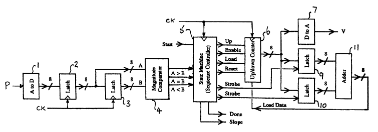
Referring to Figure 3 there is a circuit in accordance with the invention for
calibrating/operating a lithium niobate Mach-Zehnder optical modulator
(interferometer). The circuit provides a self calibrating mechanism which will
determine
values for Vo and V~ whenever the need arises. Such occasions where the
calibration of
the control voltage are required include:
~ on initial power-up of the circuitry;
~ whenever the power control loop fails fox any reason;
~ whenever the laser is turned on after a controlled shut-down;
~ on a periodic basis whenever the circuit is not carrying traffic; or
~ manually, for test purposes.
This self calibrating mechanism performed by the circuit comprises the
following steps:
CA 02437125 2003-07-31
WO 02/063381 PCT/GB02/00433
8
1. Set V = 0 and record the optical output power (PD).
2. Set V = V + ~V and record the new optical power (Pov).
3. If Pov < Po then go to step 8.
4. Keep increasing V by an amount ~V until a maximum optical power is reached.
Record Vo = the current value of V.
5. SetV=0.
6. Keep decreasing V by an amount 0V until a minimum optical power is reached.
Record V~ = the current value of V.
l0 7. Exit procedure.
8. Keep decreasing V by ~V until a maximum optical power is reached. Record Vo
=
the current value of V.
9. SetV=0.
10. Keep increasing V by an amount ~V until a minimum optical power is
reached.
Record V~ = the current value of V.
The value of Vo has already been determined from the above method. V~ is
determined
from the modulus of (VD - V~) and the polarity of the slope of the "P-V
characteristic"
is determined from the sign of Vo. It is found that a good initial condition
for the value
of V is given by the mid-point of the slope, namely:
V = (VD + V~)/2.
CA 02437125 2003-07-31
WO 02/063381 PCT/GB02/00433
9
Referring to Figure 3 the measured optical output power P is applied to an
analogue-to-
digital (A to D) converter 1 to provide a corresponding 8-bit digital value
representative
of the optical power. In Figure 3 all the connections denoted 8 indicate that
they
represent 8-bit digital connections. Typically the optical power will be
measured by
tapping a known proportion (a few %) of the total optical power output by the
modulator. This 8-bit digital representation is successively clocked into two
serially
connected latches 2, 3. As a result the value, A, held in latch 2 represents
the current
measured optical power whereas the value, B, held in latch 3 represents the
optical
power for the previous value of the control voltage V. These digital values A,
B are
to applied to magnitude comparing logic 4. The magnitude comparing logic 4 has
three
output lines respectively for the following conditions A>B, A=B, and A<B. The
respective output line is set to a high state (logic "1") in accordance with
the
comparison of the values of A and B. The output lines are used to "steer" a
controller
block 5 which in turn is used to control an up/down counter 6. The count of
the counter
6 is an 8-bit digital value representative of the current value of the control
voltage V.
This digital value is converted to an analogue voltage by a digital-to-
analogue converter
7 (D to A) whose output is analogue voltage V. This control voltage is used to
bias the
IvIZ device (not shown). The up/down counter 6 and its associated D to A
converter 7
need to operate on "signed" values since the control voltage V has to swing to
both
negative and positive values. Accordingly two's complement arithmetic is
required
here.
At the start of each "search" the up/down counter 6 is reset. During
calibration the
counter counts (up or down) until the maximum and minimum values of optical
power
CA 02437125 2003-07-31
WO 02/063381 PCT/GB02/00433
P are reached. The counts (which correspond to Vo + V~) corresponding to the
maximum and minimum values of optical power are stored in latches 9 and 10
respectively. After the counts corresponding to the maximum and minimum
optical
output have been determined the two values are added together by an adder
block 11 to
5 produce a 9-bit sum. The least significant bit of the sum discarded such
that the
resulting ~-bit value represents the mean of the two counts (i.e. corresponds
to (Vo +
V~)/2). This value is then loaded into the up/down counter 6 thereby setting
the control
voltage V to its mid-slope value, At this point the calibration process is
complete and
the controller 5 set a line denoted "done" to a high state indicating that the
calibration
to process and to initiate control of the optical modulator by a conventional
control loop.
The controller 5 also determines the polarity of the slope of the portion of
the
voltage/optical power characteristic at which the modulator has been set which
is used
by the conventional control loop during operation of the modulator. Once the
calibration circuit has determined the slope polarity and a suitable starting
point (control
voltage), its operation is disabled and the conventional control loop is
switched in.
When the calibration process is not active the conventional control loop is
used to
maintain the value of the control voltage V. Since such arrangement are known
and well
documented they are not further described here.
It will be appreciated that when it is intended to use the MZ device to
modulate optical
radiation from a laser with high-speed digital data, that the modulation drive
is disabled
during the calibration process.
CA 02437125 2003-07-31
WO 02/063381 PCT/GB02/00433
11
It will be further appreciated that modification can be made to the specific
embodiment
described which are still within the scope of the invention. For example
additional
sophistication can be added to the circuit to provide more accurate results to
take
account of noise and irregularities of the MZ device V-P characteristic. These
can
include for example:
~ measuring several samples of P (at the same value of V) and using their
average;
~ measuring several samples of P (at incrementally different values of V) and
using their average;
to ~ repeating the entire calibration process more than once and using an
average of
the findings (Vv and V~); or
~ performing a combination of the above.
Further whilst in the foregoing the circuit has been described in relation to
a MZ
interferometer the circuit and method of the present invention can be applied
to other
types of voltage controllable optical components especially those having a
voltage/optical characteristic which is periodic in character.