Note: Descriptions are shown in the official language in which they were submitted.
CA 02437443 2003-08-08
DYNAMICALLY TUNED AIVIPLiFIER FOR FREQUENCY SHIFT KEYED
SIGNALS
CROSS-REFERENCE TO RELATED APPLICATIONS
[0001] This application is a continuation-in-part of U.S. patent application
serial No.
10/288,711 filed November 5, 2002.
FIELD OF INVENTION
[4002] The present invention relates to an amplifier circuit for driving a
continuously
tunable resonant load.
BACKGROUND OF TIIE INVENTION
[000] When a highly reactive tuned load is driven by a signal at a variable
frequency, especially a fre-quency shift keyed (FSK) signal, the output
current will be
limited if the resonant frequency of the tuned load does not match the
frequency of
the drive signal. Significant energy can also be wasted if the phase of the
energy in
the tuned load for a particular bit is not synchronous with the phase of the
input signal
for a subsequent bit, i. e. at the bit transitions.
[0004] There are many applications in which it may be desirable to drive a
narrow-
bandwidth tuned load with an amplified FSK signal, such as in the generation
and
modulation of AC magnetic fields by transmitter. Such fields are used in
magnetic
inductive systems, which are employed for purposes of navigation,
communication,
signaling, direction finding and other applications.
CA 02437443 2003-08-08
_
[0005) The quasi-static AC magnetic fields used in magneto-inductive systems
are
typically generated by driving a low-frequency AC current through a tuned
antenna
formed from electromagnetic loop coils or a solenoid. ~'omer losses ~rre
minimized by
ensuring that the antenna load is a high-Q load. This has the effect of making
the
antenna load a highly-tuned narrow-bandwidth load, thereby making it difficult
to
drive effectively unless the resonant frequency of the load is matched
precisely to the
frequency of the drive signal, and the phase of the load current is not
discontinuous
with respect to the phase ofthe drive signal. When the drive signal has a
variable
frequency, such as in the case of an FSK drive signal, difficulties arise in
ensuring
that the resonant frequency of the load precisely tracks the frequency changes
of the
drive signal at bit transitions. Additionally, changes in tuning components
versus
temperature, for example, can cause detuning of the load as the ambient
temperature
changes.
SUMMARY OF THE Iht'VEI~TTI0ll~
[0006) The present invention provides a switching amplifier that drives a
tuned load
with a driving signal at a variable drive level and a variable frequency and
dynamically tunes the load to ensure. the resonant frequency of the load
matches the
frequency of the drive signal in step with any frequency transitions, thereby
providing
for efficient power transfer to the load.
[0007) In one aspect, the present system provides a circuit that includes a
tunable
resonant load containing a load energy having a load phase, a driver coupled
across
CA 02437443 2003-08-08
-3-
the tunable resonant load to apply a drive signal having a drive phase to the
tunable
resonant load to supply the load energy, a controller coupled to the tunable
resonant
load and coupled to the driver, the controller including a first component for
controlling the drive phase of the drive signal and a second componexit for
tuning the
tunable resonant load, and a feedback loop coupled between the tunable
resonant load
and the controller, the feedback loop generating an error signal in response
to a phase
deviation between the drive phase and the load phase, wherein, in response to
the
error signal, the second component generates a tuning signal for tuning the
tunable
resonant load.
[0008] In another aspect, the present invention provides a method of driving a
tunable
resonant load with an amplifier using a drive signal having a driving phase,
the
tunable resonant load containing a load energy having a load phase. ~'he
method
includes the steps of applying the drive signal to the tunable resonant load,
measuring
a phase difference between the drive phase of the drive signal and the load
phase of
the load energy, generating an error signal based upon the phase difference,
and
tuning the tunable resonant load in response to the error signal.
[0009] Other aspects and features of the present invention will become
apparent to
those ordinarily skilled in the art upon review of the following description
of specific
embodiments of the invention in conjunction with the accompanying figures.
BRIEF DESCRIPTION OF THE FIGURES
[0010] Reference will now be made, by way of example, to the accompanying
drawings which show embodiments of the present invention, and in which:
CA 02437443 2003-08-08
_ q. _
[0011] Figure I shows a block diagram of a dynamically tuned amplifier
according to
the present invention;
[0012] Figure 2 shows a more detailed block diagram of the dynamically tuned
amplifier according to the present invention;
[0013] Figure 3 shows a circuit for a full-bridge embodiment of the
dynamically
tuned amplifier according to the present invention;
[0014] Figure 4 shows a timing diagram for signals at certain points in the
circuit
shown in Figure 3;
[0015] Figure 5 shows a circuit for a half bridge configuration of the.
dynamically
tuned amplifier according to the present invention;
[0016] Figure G shows, in block diagram form, an embodiment of a circuit for
continuous reactive impedance control, according to the present invention;
[0017] Figure 7 shows a tank circuit with a variable reactive impedance,
according to
the present invention;
[0018) Figure 8 shows current and voltage waveforms for an embodiment of a
circuit
for continuous reactive impedance control, according to the present invention;
[0019] Figure 9 shows further current and voltage waveforms for an embodiment
of a
circuit for continuous reactive impedance control, according to the present
invention;
and
[0020] Figure 10 shows, in block diagram form, an embodiment of a dynamically
tuned amplifier, according to the present invention.
CA 02437443 2003-08-08
[0021] Similar reference numerals are used in different figures to denote
similar
components.
DETAILED DESCTtIP'fI01~1 OF AN EMBODIMENT
(0022] Reference is first made to Figure 1, which shows a block diagram of an
amplifiex 10 according to the present invention. The amplifier 10 includes a
tuned
resonant load 12 driven by a driver 14. The tuned resonant load 12 includes a
resonant circuit 16 having a resonant frequency determined by the reactive
components contained in the resonant circuit 16, The tuned resonant load 12
also
includes a reactance 18 and a switch 20 coupled to the resonant circuit 16.
When.the
switch 20 is closed, the reactance 18 is coupled to the resonant circuit 1G
thereby
changing its reactance and, thus, its resonant frequency.
[0023) The tuned resonant load 12 is continuously tunable through a range of
frequencies between the resonant frequency of the resonant circuit 16 on its
o~m,
through to the resonant frequency of the resonant circuit 16 when it is
coupled to the
reactance 18. To obtain a tuned resonant load 12 having a continuously
variable
resonant frequency, the reactance 18 is coupled to the resonant circuit 16 for
a
symmetrical portion of a quarter-cycle at the beginning and preceding 'the end
of each
half cycle of the oscillating frequency. The portion may vary from zero to a
full
quarter-cycle. Such a method and apparatus for obtaining a tuned resonant load
12
with a continuously variable resonant frequency is detailed below with
reference to
Figures 6 through 10.
CA 02437443 2003-08-08
..
[0024] The driver 14 supplies power to the tuned resonant load 12 to drive its
load
current. For maximum efficiency, the resonant frequency of the tuned resonant
load
I2 should match the frequency of a drive signal supplied by the drive 14.
Drive
signals that are not at the resonant frequency of the tuned resonant load 12
will be
only partially effective in delivering current to the tuned resonant load 12.
Additionally, the phase of the load current and of the drive signal should be
the same
for achieving maximum load current in the tuned resonant load 12. Furthermore,
at
step changes in the frequency of an FSK drive signal, the tuned frequency of
the tuned
resonant load 12 and the phase of the load current should match the frequency
arid
phase of the FSK drive signal.
[0025] In one embodiment, the driver 14 supplies energy by way of a bipolar
pulsed
voltage signal 24. Because the tuned resonant load I2 is a highly tuned
circuit, i.e, a
high-Q circuit, the harmonics of load current are significantly attenuated
leaving a
substantially sinusoidal waveform for the Load current. Accordingly, the
harmonics of
the bipolar pulsed voltage signal 24 are filtered by the tuned resonant load
12
resulting in a predominantly sinusoidal load current at the fundamental
frequency.
[0026] The switch 20 and the driver l4 operate in response to a controller 22.
The
controller 22 coordinates the opening and closing of the switch 20 so as to
appropriately tune the tuned resonant load I2 to a particular resonant
frequency far
each half cycle. The controller 22 also controls the driver 14, including
setting the
frequency of the bipolar pulsed voltage signal 24 and controlling the pulse
width of
the bipolar pulsed voltage signal 24. By controlling the pulse width, the
controller 22
controls the quantity of energy supplied to the tuned resonant load 12. To
prevent
pulling or pushing tile oscillation frequency (i.e., retarding or advancing
the phase
CA 02437443 2003-08-08
7 ..
angle) of the tuned resonant load 12, the controller 22 includes a function or
routine in
its firmware that ensures that the driver 14 centers each positive and
negative voltage
pulse in the half cycle of the tuned resonant load 12 current. In order to
ensure this
centering occurs, the controller 22 includes a function or routine that tunes
the
resonant frequency of the tuned resonant load 12, so that its resonant
frequency
matches the frequency and phase of the bipolar pulsed voltage signal 24 with
which it
is being driven.
[0027] The controller 22 receives information through a feedback Loop 26 from
the
tuned resonant load 12, upon which it may make adjustments to its control of
the
switch 20, thereby fine-tuning the resonant frequency of the tuned resonant
load 12.
The feedback information 26 may include voltage or current zero crossings from
various points in the tuned resonant load 12 ar other indicators of phase or
frequency.
[0028] The controller 22 may be implemented using a microcontroller suitably
programmed to execute a program in firmware to perform the functions,
calculations
and routines described herein. It may also be implemented using oscillators,
comparators and various other logic circuits and discrete components, or a
combination of such components and a microcontroller. Other methods of
implementing the various controller 22 functions will be apparent to one of
ordinary
skill in the art in light of the description herein.
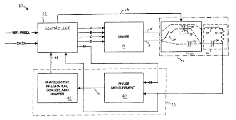
[0029] Reference is now made to Figure 2, which shows a more detailed block
diagram of an embodiment of the dynamically tuned amplifier 10 according to
the
present invention, and to Figure 4, which shows exemplary timing diagrams for
various signals in the amplifier 20.
CA 02437443 2003-08-08
(0030] The amplifier 10 includes the tuned resonant load 12 and the driver 14,
which,
in this embodiment, is a full-bridge configured driver. The driver 14 includes
a left-
side drivepoint H1 and a right-side drivepoint H2 that are coupled to the
tuned
resonant load 12. The driver l 4 operates in a push-pull mode as each of the
two sides
H1 and H2 are alternately driven with complementary pulse signals.
[003I] The tuned resonant load 12 includes the resonant circuit 16 which
includes an
inductive coil 28 in series with a base capacitance 30. The inductive coil 28
and other
elements of the tuned resonant load 12 will include a certain amount of
resistive
impedance, shown as resistor 32.
[0032] The tuned resonant load 12 further includes a tuning apparatus 34. The
tuning
apparatus 34 includes a second capacitor 36 in series with the base capacitor
30. The
tuning apparatus also includes the switch 20 and the reactance 18, which in
this
embodiment is a tuning capacitor 38. The combination of the switch 20 and the
tuning capacitor 38 are connected in parallel with the second capacitor 36.
The ratios
of the capacitors 38, 36, and 30 determine the tuning range.
(0033] In this configuration, if the switch 20 is open, the resonant frequency
of the
taxied resonant load 12 is an upper frequency, which is determined by the
inductive
coil 28, the base capacitor 30 and the second capacitor 36. If the switch 20
is closed,
then the resonant frequency of the tuned resonant load 12 is a lower
frequency, which
is determined by the foregoing elements plus the tuning capacitor 38. If the
switch 20
is only closed for a portion of a quarter-cycle at the beginning and end of
each half
cycle of the resonant voltage across the tuning capacitor 38, then the
resonant
frequency of the tuned resonant load 12 will be between the lower frequency
and the
upper frequency and will be adjustable through varying the duration of the
portion, as
CA 02437443 2003-08-08
detailed below with reference to Figures 6 through 10. Accordingly, the tuned
resonant load 12 has a continuously variable resonant frequency, the value of
which is
determined by the controller's 22 operation of the switch 20.
[0034) The driver 14 receives digital FSK signals A, B, C, and D from the
controller
22. The controller 22 generates the FSK signals A, B, C, and D at the
appropriate bit
rate and frequency for controlling each quarter of the full-bridge driver 14.
Exeuiplary waveforms for the FSK signals A, B, C, and D are shown in Figure 4
and
are described in greater detail below. The FSK signals A, B, C, and D
determine the
complementary pulse signals produced at the two side drivepoints Hl and H2 of
the
driver I4. The complementary pulse signals at the two drivepoints H1 and H2
result
in a bipolar pulsed drive voltage across the bridge.
[0035] The signal generating aspect of the controller 22 may be implemented by
an
oscillator and tuning and logic circuits. It may also be implemented through a
program or module for execution by a microprocessor or other means, as will be
understood by those of ordinary skill in the art.
[0036] The controller 22 receives a reference frequency signal from which the
frequency of the FSK signals A, B, C, and D may be derived and a data signal.
The
data signal contains the binary information with which the FSK signals A, B,
C, and
D are modulated. The binary FSK signals A, B, C, and l7 are generated at
either a
first frequency or at a second frequency, depending upon whether the data
signal
indicates a zero or a one.
[0037] Tn addition to generating the FSK signals A, B, C, and D for
controlling the
driver 14, the controller 22 generates a capacitor switch signal 23 for
controlling the
opening and closing of the switch 20 in the tuning apparatus 34. Through the
CA 02437443 2003-08-08
- l~ -
capacitor switch signal 23, the controller 22 controls the resonant frequency
of the
tuned resonant load 12. The controller 22 adjusts the resonant frequency of
the tuned
resonant load 12 to dynamically match the frequency of the FSK signals A, B, C
and
D, and, accordingly, the fundamental frequency of the bipolar pulsed drive
voltage for
driving the tuned resonant load 12. In this manner, the controller 22 ensures
that the
driver 14 drives the tuned resonant load 12 efficiently to achieve the desired
load
current by driving the load 12 with an input frequency to which the resonant
frequency of the tuned resonant load 12 is matched. Moreover, as the driving
frequency changes during bit transitions in the FSK signal, the controller 22
alters the
resonant frequency of the tuned resonant load 12 to dynamically track the
frequency
of the drive signal and to maintain the phase of the load current and the
phase of the
drive signal the same 'within a small error.
[0038] The controller 22 may be provided with a memory that stores preset
capacitor
switch signal 23 settings for particular driving frequencies., enabling the
controller 22
to rapidly adjust the resonant frequency of the tuned resonant Ioad 12 at bit
transitions
and then rely upon the feedback loop 26 to make any subsequent fine tuning
adjustments to compensate for component drift in the tuned resonant load 12.
The
settings stored in the memory may be updated periodically., such as at each
bit
transition, to reflect the most recent capacitor switch signal 23 setting for
a particular
driving frequency.
(0039] The controller 22 also generates a master signal M, which is a digital
FSK
square wave with a 50% duty cycle during each bit interval. An exemplary
waveform
for the master signal M is also depicted in Figure 4. The master signal M
contains the
desired FSK frequency shifts derived from the bit changes in the data signal.
'The
CA 02437443 2003-08-08
-11-
master signal M is related to the FSK signals A, B, C, and D in that thosE;
latter
signals determine the bipolar pulsed drive voltage across the bridge and the
master
signal M has zero crossings centered between each pair of bipolar pulses. The
master
signal M is 180 degrees out of phase with the drive voltage across the bridge.
The
controller 22 ensures that the current in the tuned resonant load 12 is in
phase with the
bipolar pulsed drive voltage. Accordingly, the master signal M will also be
180
degrees out of phase with the current in a load that is tuned to resonance. As
a proxy
for load current phase, the phase of the voltage across the tuning capacitor
38 will lag
the current by 90 degrees, meaning that it will lead the master signal M lby
90 degrees
when the frequency of the tuned resonant load I2 is tuned to match the
frequency of
the drive signal. The master signal M serves as a reference phase for
comparison v~~ith
the phase of the capacitor voltage in a phase comparator 40 whose mid-control
point
occurs at a 90 degree phase difference at its inputs.
[0040] The phase comparator 40 produces a signed phase error signal 41. The
phase
error signal 41 is centered upon a desired 90 degree phase difference. Each
half
cycle, the phase of the voltage across the capacitors 30, 36 or 38 is compared
with the
phase of the master signal M. If the phase differs by more than or less than
90
degrees, the signed phase error signal 41 indicates the level of phase advance
or
retard.
(0041] The phase error signal 41 is input into a feedback generator 42, which
includes
an integrator and a gain block. The integrator and gain block implement a
scaling and
damping function for smoothing out the phase error signal 41 and generating a
delay
control signal 43. The delay control signal 43 is input into the controller
22, which
CA 02437443 2003-08-08
- 12-
uses the delay control signal 43 to determine in appropriate capacitor switch
signal 23
in order to tune the tuned resonant load 12, so as to minimize the phase
error.
[0042] The phase comparator 40 and feedback generator 42 may be implemented
using discrete components, discrete logic devices, a suitably programmed
microprocessor, or through other means. They may also be implemented as a part
of
the controller 22 using a microcontroller or microprocessor. The parameters of
the
functions may be determined in conjunction with the natural time constant of
the
tuned resonant Ioad 12 to ensure rapid settling of the load current when the
driver 14
is activated.
(0043] Reference is next made to Figures 3 and 4. Figure 3 show Ts a circuit
for a full-
bridge embodiment of the dynamically tuned amplifier 10. Figure 4 shows an
exemplary timing diagram 100 for certain signals in the amplifier 10 shown in
figure
3.
[0044] As can be seen from Figure 3, the driver 14 includes a left upper
switch, a left
lower switch, a right upper switch, and a right lower switch. In this
embodiment, the
four switches are most readily implemented using a left upper MOSFET .50, a
left
lower MOSFET 52, a right upper MOSFET 54, and a right lower MOSFET 56,
respectively, all of them being N-channel devices. In other embodiments, the
switches rnay be implemented using integrated gate bipolar junction
transistors, P and
N-channel MOSFETs with appropriate drivers, relays or other switching
mechanisms
selected to be appropriate for the current and voltage to be delivered to the
tuned
resonant load 12.
[0045] Each MOSFET 50, 52, 54 and 56, is coupled to a respective FET driver
70,
72, 74 and 76. The source of the left upper MOSFET 50 is connected to the
drain of
CA 02437443 2003-08-08
-13-
the left lower MOSFET 52 to form the left side of the driver 14. Similarly,
the source
of the right upper MOSFET 54 is connected to the drain of the right lower
MOSFET
56 to the form the right side of the driver 14. Accordingly, the left
drivepoint Hl of
the driver 14 is between the two left NIOSFETs 50, 52 and the right drivepoint
H2 of
the driver 14 is between the two right MOSFETs 54, 56. Connected between the
two
drivepoints Hl; H2 is the tuned resonant load 12 to be driven by the driver
14. In this
embodiment, the tuned resonant load 12 includes the resonant circuit 16
together with
the tuning apparatus 34.
[0046] The drain of the left upper MOSFET 50 and the drain of the right upper
MOSFET are both connected to a positive rail 44 of the DC power source for the
amplifier 10. The sources of the two lower MOSFETs 54, S6 are connected to a
negative rail 46 of the pov,-er source.
[0047] In full power operation, each side of the driver 14 is driven in a push-
pull
mode with complementary square-wave signals. The FET drivers 70, 72, 74, and
76
receive input signals A, B, C, and D, respectively. Input signals A and I3 are
complimentary such that only one of the left side MOSFE'rs 50, 52 is on at a
time.
Similarly, input signals C and D are complimentary such that only one of the
right
side MOSFETs 54, 56 is on at a time. For operation, input signals A and D are
in
phase, such that when the left upper MOSFET 50 is on or off, so is the right
lower
MOSFET 56, and input signals B and C are in phase, meaning that left lower
MOSFET 52 and the right upper MOSFET 54 turn on and off at the same time.
Accordingly, when input signals A and D turn on the left upper and right lower
MOSFETs 50, 56, the left drivepoint H1 is coupled to the positive voltage rail
44 and
the right drivepoint H2 is coupled to the negative voltage rail 46. When input
signals
CA 02437443 2003-08-08
-I4-
B and C turn on the left lower and right upper A~IOSFETs 52, 54, the left
drivepoint
Hl is coupled to the negative voltage rail 46 and the right drivepoint H2 is
coupled to
the positive voltage rail 44. This allows the driver 14 to create a bipolar
square wave
102 across the drivepoints HI, H2.
[0048] By making small delays in the rising edges of input signals A, B, C,
and D,
provision is made to ensure that MOSFETs 50 and 52, and MOSFETs 54 and 56, are
not turned on together during the onloff transition.
[0049] The load will be driven efficiently if the input signals A, B, C and D
have the
same frequency as the frequency of the tuned load. With a highly tuned load,
the
harmonics of the bipolar pulsed voltage signal are filtered by tile tuned load
resulting
in a sinusoidal load current at the fundamental frequency.
[0050] In order to limit switching transients that could damage the MOSFETs
50, 52,
54, and 56, low-inductance connections are used bet~~een the components of the
driver I4, and low-impedance decoupling is used for the DC: power supply
voltage
across the drivepoints Hl, I-I2 during switching. Accordin,giy, to provide
decoupling,
the amplifier I O features a set of low-frequency and high-frequency
decoupling
capacitors 48 coupled between the positive rail 44 and the negative rail 46 of
the
power supply. In addition, the MOSFETs 50, 52, j4, and 56 each have a
respective
low-inductance commutation diode 60, 62, 64, and 66 connected from source to
drain
to provide a path for transient pulses in load current. The commutation diodes
60, 62,
64, and 66 are also for carrying decaying load current during a normal shut-
down, and
in the event of drive failure.
[0051] The driver 14 shown in Figure 3 provides variable output power to the
tuned
resonant load 12 tluough varying the pulse width of the bipolar square wave
102
CA 02437443 2003-08-08
-15-
across the drivepoints H1, H2. This is accomplished by varying the extent to
which
input signals A and B are in phase with input signals D and C, respectively.
As
outlined above, to operate at full power, the driver 14 requires input signals
A and D
to be in phase and input signal B and C to be in phase. Ho'~,~ever, in this
embodiment,
input signals C and D have an initial state of being 180 degrees out of phase
with
input signals B and A, respecti~,rely. Under these circumstances input signal
C is
completely out of phase with input signal B, and input signal A is completely
out of
phase with input signal D, meaning that the appropriate MOSFET 50, 52, 54, and
56
pairs are being driven completely out of sync and supply no current to the
tuned
resonant load 12.
(0052] Under the command of the controller 22, the input signals C and D may
be
delayed by up to one-half cycle. A full delay of one-half cycle would bring
input
signals C and D into phase with input signals B and A, respectively, resulting
in
maximum load current. The delay is adjustable between zero and one-half cycle
and
the extent of the delay determines the pulse width of the bipolar square wave
102
across the tuned load 12.
[0053] As may be seen in Figure 4, by initially having the drive signals to
each side
of the driver 14 bridge out of phase and then applying a variable delay, the
extent to
which the two sides of the bridge correspond is variable, resulting in a
i>ipolar square
wave 102 with a variable pulse width. The pulse width of the bipolar square
wave
102 corresponds to the amount of the delay. The pulse width of a positive
pulse 104
of the bipolar square wave 102 is determined by the overlap of input signals A
and D,
since this will correspond to the time during which both the left upper MOSFET
50
and the right lower MOSFET 56 are both on. Similarly, the pulse width of a
negative
CA 02437443 2003-08-08
- 16-
pulse 106 of the bipolar square wave 102 is determined by the overlap of input
signals
C and B.
[0054] As also sho~~n in Figure 4. the coil current 108 is filtered by the
tuned load 12
to remove harmonics from the bipolar square wave 102 driving the tuned load
12;
leaving a substantially sinusoidal coil current 108 at the fundamental
frequency and
similarly a sinusoidal capacitor voltage 110.
[0055] Note that the pulses 104, 106 of the bipolar square wave I02 are
symmetrical
and are centered within the half cycles of the coil current 108 when the tuned
resonant
load 12 is correctly tuned. Vfhen the frequency of the input signals A, B, C,
and D
changes in response to a change in the FSK data signal, the resonant frequency
of the
tuned load 12 is adjusted so as to match the frequency of the input signals A,
B, C,
and D. In order to make this adjustment to the frequency of the tuned load 12,
the
edges of data bits are made coincident with zero-crossings of the capacii:or
voltage
110. In other words, bit transitions, i. e. changes in frequency, occur during
zero-
crossings of the capacitor voltage 110.
(0056) Referring still to Figure 3, the controller 22 (Fig. 2) receives
feedback
information from the tuned load l2 through a current sensor 80 that measures
the
current flow in the tuned load 12 and through a voltage sensor 82 that
measures the
capacitor voltage. Accordingly, the controller 22 is able to recognize zero-
crossings
of the current and voltage. The capacitor voltage measured by the voltage
sensor 82
in particular is input to the phase comparator 40 (Fig. 2) along with the
master signal
M to ensure that it leads the master signal M by 90 degrees. In other
ernbodirz~.ents,
the capacitor voltage may be sensed using other voltage sensors, such as, for
example,
a transformer coupled across the base capacitor 30.
CA 02437443 2003-08-08
- 1'7 -
[0057] Those skilled in the art will understand that, in this embodiment, the
capacitor
voltage is a proxy used to assess the extent to which the frequency and phase
of the
energy in the tuned load 12 correspond to the frequency and phase of the drive
signal.
Other mechanisms for measuring the current or voltage in the tuned load 12 in
order
to sense the frequency and phase of oscillation will be familiar to those of
ordinary
skill in the art.
[005] Reference is now made to Figure 5, uJhich shows a circuit for a half
bridge
configuration of the dynamically tuned amplifier 10. In this embodiment, the
driver
14 includes the left-side MOSFETs 50 and 52. Input signals A and B directly
control
the operation of the driver 14 azld the application of power to the tuned load
12.
[0059] In order to obtain control over the output load current in the circuit
of Figure
5, direct control over the pulse width of A and B is necessary. The controller
22
symmetrically reduces the width of the pulses of input signals A and B to
create the
desired bipolar drive voltage across the tuned load 12.
[0060] Reference is now made to Figure 6, which shows a block diagram of a
circuit
11 for continuous variable reactive impedance control, according to the
present
invention. The circuit 11 may be employed in a dynamically-tuned amplifier
according to the present invention to provide a tuned load with a continuously
variable resonant frequency. The circuit 11 includes the tuned load 12 and the
controller 22. As described above, the switch 20 controls whether the
reactance 18 is
coupled to the resonant circuit 1 ~. The operation of the switch 20 is
controlled by the
controller 22. The controller 22 is coupled to the resonant circuit 16 through
the
feedback loop 26 to obtain data that tnay influence the opening or closing of
the
switch 20.
CA 02437443 2003-08-08
-18-
[0061] The reactance 18 is a reactive impedance that is selectively 'coupled
to the
resonant circuit 16 through the closure of the switch 20 as will be described
in more
detail below. When the reactance 18 is coupled to the resonant circuit 16, the
impedance of the resonant circuit 16 is changed. Far a resonant circuit 16
having a
natural resonant frequency, such as an LC circuit, the addition of the
reactive
component 12 will change the natural resonant frequency.
(0062] Reference is now made to Figure 7, which shows an embodiment of the
circuit
11 with a variable reactive impedance, according to the present invention. In
the
embodiment shown in Figure 7, the resonant circuit 16 includes the inductive
coil 28
coupled in parallel with a base capacitance 30. T his configuration may be
referred to
as a "tank circuit". The inductive coil 28 and the base capacitance 30 set the
natural
resonant frequency of the resonant circuit I6.
[0063] The reactance 18 is a tuning capacitor 38. The tuning capacitor 38 is
coupled
in parallel with the base capacitance 30, through the switch 20. With the
switch 20
open, the tuning capacitor 38 is disengaged frown the circuit I I and does not
impact
the resonant circuit 16. u.Then the switch 20 is closed, the natural resonant
frequency
of the resonant circuit 16 is altered due to the additional capacitance.
Through the
operation of the switch 20, in accordance with the present invention, the
circuit 1 I
provides continuously variable impedance and a corresponding continuously
variable
natural resonant frequency o~~er a range of frequencies, as will be described
below.
[0064] As will be apparent to those of ordinary skill in the art, various
oi;her passive
components, including resistors, additional capacitors or additional
inductors, or
active components, including transistors, op-amps or other components may be
added
CA 02437443 2003-08-08
-19-
to the circuit 11 to customize it to a particular application requiring a
particular
impedance or other specific characteristics.
[0065] The continuously variable adjustment of the impedance and frequency of
a
circuit according to the present invention is now illustrated 'with reference
to Figure 8,
which shows current and voltage: waveforms for the circuit 11 of Figure 7. In
particular, Figure 8 shoes a graph 200 of voltage and current versus time:.
The graph
200 includes a first voltage waveform v~ for the base capacitance 30 (Fig. 7),
a second
voltage waveform vs~ for the tuning capacitor 38 (Fig. 7) and a current
waveform io
for the inductive coil 28 (Fig. 7). The waveforms v~, vs~, and io are each
approximately sinusoidal.
[0066] As the graph 200 shows, the tuning capacitor 38 is Engaged in the,
circuit 11
(Fig. 7) between time to and time tI, for a duration dt. In other words, the
switch 20
(Fig. 7) is closed between time try a.nd time t~. The switch 20 is then opened
at time t~,
disengaging the tuning capacitor 38 from ti;ne t~ to time t2. It remains
disengaged
until time t;, when it is re-engaged for the duration of the half cycle which
ends at
time t4. The duration dt of time tl - to is the same as the duration of time
t4 - t3. In
other words, the switch 20 is opened at time tl and closed at time t3,
removing the
tuning capacitor 38 from the circuit 11 for the duration t3 - tI, centered
within the half
cycle.
[0067] Beginning at time to, the current through the inductive coil 28 is at a
maximum
and the voltage of the capacitors 24 and 26 is at zero. The base capacitance
30 and
the tuning capacitor 38 begin to accumulate charge, as reflected in the
voltage
waveforms v~ and vS~, and the current in the inducti~~e coil 28 begins to
decrease, as
shown in the current waveform io. After duration dt, at time t;, the switch 20
is
CA 02437443 2003-08-08
-20-
opened, disengaging tuning capacitor 3 8 from the cixcuit 11. Accordingly, it
accumulates no further charge and maintains its voltage potential, as shown by
the
second voltage waveform vs~. The voltage of the base capacitance 30 continues
to
increase in substantially sinusoidal fashion, reaching a peak at time t2. This
corresponds with the zero-crossing of the current waveform i~, indicating zero
current
in the inductive coil 28,
[0068] After time t2, the voltage of the base capacitance 30 begins to
decrease as
shown in the first voltage wavefonn v~. At time t3, the voltage of the base
capacitance
30 matches the voltage of the tuning capacitor 38, at which point the tuning
capacitor
38 is re-engaged in the circuit 10. From time t3 to time t4, the two
capacitors 24 and
26 discharge together. At time t:~, both capacitors 24 and 26 have fully
discharged, as
shown by the zero-crossing of the two voltage waveforms v~ and vs;;. The
duration dt
is the same between times to and t~ and between times t3 and t4.
[0069] The time t_; may be calculated in order to determine when to switch the
tuning
capacitor 38 back into the resonant circuit 16, or the voltages on the base
capacitance
30 and the tuning capacitor 38 may be compared and the tuning capacitor 38 may
be
re-engaged when the voltages are identical, which will occur at time t3. If
the tuning
capacitor 38 is re-engaged on the basis of a voltage comparison, then in one
embodiment it may be done through sensing the voltage on each capacitor and
using a
comparator to trigger the switch 20 to close. Other possible methods will be
understood by those skilled in the art:
[0070] Following time t4, the switch 20 remains engaged and the process
repeats
itself, but with reversed polarity. The switch 20 is closed for a duration dt
at the
CA 02437443 2003-08-08
-21 -
beginning and at the end of the second half cycle, and open in between those
durations.
[007I] By varying the duration dt, and therefore the times tr and t3, the
resulting
oscillation frequency of the circuit may be altered. This is further
illustrated with
reference to Figure 9, which shows a graph 210 of current a.nd voltage
w~aveforms for
the circuit 11 (Fig. 7).
[0072] Figure 9 shows a waveforrn for the voltage v~ across the inductive coil
28.
The current through the inductor is depicted as the waveform io. Also shown
are two
sinusoids: a first voltage sinewave vl and a second voltage sinewave v2.
Sinewave vl
varies at the natural resonant frequency of the circuit 11 (Fig. '~) when the
tuning
capacitor 38 (Fig. 7) is engaged. Sinewave v2 varies at the natural reson<rnt
frequency
of the circuit 11 when the tuning capacitor 38 is not engaged. Note that
sinewave vz is
depicted with a phase shift cp, for reasons which will become apparent from
the
following description.
[0073] As described above, the circuit 11 begins each half;cycle of its
oscillation
frequency with the switch 20 (Fig. 7) closed and, thus, the tuning capacitor
38
engaged. Under these circumstances, the voltage vo across the inductive coil
28 (Fig.
7) changes in accordance with sinewave vr, which correspo~ads to the natural
resonant
frequency of the circuit 11 when the inductive coil 28 is in parallel with the
base
capacitance 30 (Fig. 7) and in parallel with the tuning capacitor 38.
[0074] At time tl, with the voltage vo at a magnitude of Vr, the tuning
capacitor 38 is
switched out of the circuit 1 l, thereby changing the natural resonant
frequency of the
circuit 11. The resonant frequency of the circuit 11 is now determined by the
inductive coil 28 in parallel with the base capacitance 30 alone. This
frequency is
CA 02437443 2003-08-08
-22-
reflected in sinewave v2. At time tl, the voltage vo across the inductive coil
28 stops
following sinewave v~ and starts changing in accordance with sinewave v2. As
can be
seen in Figure 9, sinewave v2 has a higher frequency than sineu~ave v~. The
phase
shift cp shown in sinewave v2 is necessary to ensure the condition that
sinewave v2 has
a magnitude of V l at time tl .
[0075] At time t3, the tuning capacitor 38 is switched back into the circuit I
l,
changing the natural resonant frequency of the circuit 11 back to the lower
frequency
of sinewave vl. Accordingly, from t3 to t.~ the voltage vo across the
inductive coil 28
changes at a rate described by sinewave v~. In Figure 9, the voltage vo can be
seen
deviating from sinewave v2 after time t3.
[0076) With time tl set between to and t2, the frequency of the voltage vo
will be
neither the frequency of sinewave v~ nor the frequency of sinewave v2, but
rather a
frequency in between. The frequency of the voltage vo may be varied by varying
the
duration dt during which the turning capacitor 38 is engaged in the circuit.
To reduce
the impact of the tuning capacitor 38 and thereby increase tile frequency of
the
voltage vo closer to the frequency of sinewave v2, the duration dt is
decreased.
Conversely, to lower the frequency of the voltage vo closer to the frequency
of
sinewave vl, the duration dt is increased. By providing for continuous
variability of
dt, the circuit 11 has a continuously variable frequency within the range:
between the
frequency of sinewave vi and the frequency of sineurave v2.
[0077] The foregoing embodiment may also be illustrated mathematically. For
example, the sinev<lave vl may be described by the equation:
vl(t) = A1 sin(co~t) (1)
CA 02437443 2003-08-08
- 23 -
(0078) In the above equation (1), At is the magnitude and ccy is the
frequency. The
magnitude A1 is the maximum voltage of the sinewave. This maximum is given by
umax = Imp Z, which in the present circuit 11 may be expressed as Iouy L. The
frequency uy is the natural resonant frequency of the circuit 11 with the
tuning
capacitor 38 included, which is described by:
1 (2)
L(Ca +C~)
[0079] The other sinewave v2 may be described by the equation:
v2 (t) = Az sin(co2t + ~p) (3)
[0080] The frequency c~2 is given by the natural resonant frequency of the
circuit 10
with the tuning capacitor 38 disengaged, which is described by the equation:
1
~z = L,C~ (4)
[0081] The maximum magnitude A2 of sinewave v2 can be determined from the
assumption of conservation of energy. The total energy in the circuit 10 at
time t~ is
due to the maximum current Io in the inductor L. When the tuning capacitor 38
is
s«.~itched out of the circuit 10 at time t~ it has a specific quantity of
energy stored in it.
At time t2, the total energy that had been in the inductor at time to is now
contained in
the two capacitors 24 and 26. The voltage on the base capacitance 30 at time
tz is the
maximum voltage, or the magnitude, A2. From this we can equate the total
energy at
time to to the total energy at time t2 in the expression:
'ZLIo ='zC~v~(t~)z -~/Cbvz(tz)z (5)
CA 02437443 2003-08-08
-24-
A 2 = vz (tz ) = LI o - Cay (ti )z (6)
b
[0082] At time tl it is ltnown that vt(t~) = v2(t~) = A2sin (~Z t~ + ~p).
Therefore, the
phase shift ~ may be expressed as:
tp = arcsin vAt' ) - coZt~ (7)
z
[0083] It is also known that at time t2, v2(t) is at a maximum. Therefore, the
sinusoidal component of v2(t) is equal to l, meaning that sin (cot t2 + rp) ==
sin (~/2) _
1. Therefore t2 may be expressed in terms of a~2 and gyp. Of course, the t me
t2 is
related to the oscillation frequency of the circuit f~.
[0084] Using the above expressions, the oscillation frequency f~ can be
related
entirely to L, C~,, Cb and tl. If the values of L, Cd, and C~, are known, then
the
oscillation frequency f~ produced by a particular ti may be calculated.
T~Ioreover, to
achieve a particular oscillation frequency f~, the appropriate time ta, and
thus the
duration dt, may be calculated.
[0085] Reference is now made to Figure 10 which shows, in block diagram form,
an
embodiment of the dynamically tuned amplifier 10, according to the present
invention. As opposed to the tank circuit 11 shown in Figure 7, which featured
the
inductive coil 28 and base capacitance 30 in parallel, the amplifier 10 shown
in Figure
features the inductive coil 28 and the base capacitance 30 coupled in series.
The
tuning capacitor 38 is coupled in parallel with the base capacitance 30
through the
switch 20. The second capacitor 26 is coupled in series between the base
capacitance
30 and the inductive coil 28. The values of the three capacitors 24, 25, 26
and of the
CA 02437443 2003-08-08
-25-
inductive coil 28, set the range of adjustability of the natural resonant
frequency of the
amplifier 10 and the acceptable voltage and current values for the circuit.
The
addition of, and size of, the second capacitor 26 may be necessitated by the
current or
voltage rating of the switch 20.
[0086] The switch 20 is controlled by the controller 22, which is coupled to
the
feedback loop 2b. The switch 20 comprises a pair of FETs Q 1 and Q2 having
their
sources connected together. The drain of the first FET Q 1 is connected to the
tuning
capacitor 38 and the drain of the second FET Q2 is connected to the base:
capacitance
30. The gates of the FETs Ql and Q2 are coupled to the controller 22. The
switch 20
further includes first and second diodes D 1 and D2. The first diode D 1 is
coupled
across the first FET Q 1 and the second diode is coupled across the second FET
Q2.
The anodes of the diodes D l and D2 are connected to the sources of the FETs Q
1 and
Q2. The cathode of first diode D 1 is connected to the drain of first FET Q 1
and the
cathode of second diode D2 is connected to the drain of second FET Q2.
[0087] At a voltage zero-crossing, the switch 20 is in a closed state, meaning
that both
FETs Q 1 and Q2 are switched on. This requires that the controller 22 provide
a signal
to the gates of the FETs Q 1 and Q2. After the duration dt, at time tz, one of
the FETs
Q 1 or Q2 is switched off by the controller 22. Which FET Q 1 or Q2 is
switched off
depends upon the polarity of the voltage waveform. Diodes D 1 and D2 may
conduct
when their respective FET Ql or Q2 has been switched off if the voltage across
the
FET Ql or Q2 from drain to source is back biased. In other words, once the
voltage
on the base capacitance 30 has discharged to a level equal to or just less
than the
voltage on the tuning capacitor 38, the diode Dl or D2, depending on the
polarity,
permits the tuning capacitor 38 to begin discharging together with the base
CA 02437443 2003-08-08
-26-
capacitance 30. Accordingly, in this embodiment, the switch 20 re-engages the
tuning
capacitor 38 at the appropriate time t3. The switch 20 remains closed for a
duration dt
at which point a voltage zero-crossing will occur, and the process will
repeat. The
effects of the diode voltage drop may be ignored in high current and high
voltage
applications. Although many FETs, and aVIOSFETs in particular, integrally
feature
diodes like diodes D 1 and D2 by virtue of the physical consl:ruction of the,
FET, the
additional diodes D 1 and D2 are added in the present embodiment because they
are of
better quality and reliability than the internal diodes of a FET. In lower
power
application, it may be possible to rely solely upon the internal diodes of the
FETs.
[0088] The controller 22 includes a microcontroller 90 and a set of FET
drivers 92.
The FET drivers 92 axe coupled to the gates of the FETs Q 1 and Q2 and provide
the
signals required to turn the FETs Q 1 and Q2 on or off, The FE'h drivers 92
are
controlled by the microcontroller 90.
[0089] The microcontroller 90 determines when to open and close the switch 20.
In
other words, the microcontroller 90 determines the duration dt du.ring which
the
switch 20 is to remain closed at the beginning and end of each half cycle of
the
oscillation frequency of the amplifier 10. As outlined above, in this
embodiment, the
microcontroller 90 causes the switch 20 to open after the expiry of the
duration dt
following a zero-crossing of the voltage and the switch 20 closes itself at a
time dt
before the end of the next zero-crossing,
[0090] Coupled to the microcontroller 90 through the feedback loop 26 is a
zero-
current detector 94 and a zero-voltage detector 96. 'The zero-voltage detector
96
provides the microcontroller 90 with a signal indicating the zero-crossing
points and
polarity of the voltage in the amplifier 10. From this information, the
microcontroller
CA 02437443 2003-08-08
_ 2~ -
90 can identify the time to and the time t4, and therefore the oscillation
frequency of
the amplifier 10. The microcontroller 90 may then calculate the time t~ and
the time t3
at which to open and close the switch 20; based upon the duration dt:
[0091] The zero-current detector 94 provides the microcontroller 90 with a
signal
indicating the zero-crossing points and polarity of the current in the
inductive coil 28.
From this data, the microcontroller 90 can assess the extent to which the
voltage and
current are 90° out of phase, which represents the desired phase shift
in a resonant
circuit.
[0092] The microcontroller 90 also controls the driver 14 that is coupled to
the
inductive coil 28 and the base capacitance 30. ~s described above with
reference to
Figures 1 through 5, the driver 14 may be an H-bridge configuration. The
driver 14
drives oscillation of the amplifier 10 by supplying a drive signal to the
inductive coil
28 and base capacitance 30. l,he drive signal may be an FSI~ square wave that
varies
in frequency in accordance with the inf ormation encoded therein. T he
microcontroller 90 adapts the resonant phase and frequency of the amplifier 10
to so
as to match the phase and frequency of the drive signal and thereby improve
the
efficiency of the amplifier 10.
[0093] The efficiency of the amplifier 10 will depend upon the match between
the
resonant frequency of the tuned load and the frequency of the driver signal
with which
it is being driven. The microcontoller 90 can determine the extent of such a
match
through a phase comparison between the voltage and the current of the
amplifier 10,
as provided by the feedback loop 26. It may then adjust the impedance, and
thus the
resonant frequency, of the amplifier 10 through adjusting the duration dt in
order to
more accurately match the resonant frequency to the drive frequency.
CA 02437443 2003-08-08
-28-
[0094] An amplifier that is set to be driven at a predetermined frequency and
is
optimized to operate at that frequency may experience ineffvciencies ifthere
is any
drift in the components, such as the inductance. tine-tuning of the amplifier
10
through alteration of the duration dt can re-establish the efficiency of the
amplifier 10.
This may find application in antennas, amplifiers or other oscillating
circuits. Such a
circuit or method may also be used with existing systems to re-tune and
optimize their
performance.
[0095] The microcontroller 90 is suitably programmed to execute a program in
firmware to perform the functions and calculatians described herein. The
programming will be within the understanding of those ordinarily skilled in
the art of
microcontroller programming.
[0096] The microcontroller 90 may include a memory having one or more preset
durations dt corresponding to present oscillation frequencies.
[0097] The present invention may be incorporated in a transmission system,
such as a
magnetic inductive transmitter, receiver or transceiver. Such a system may
include an
antenna and other elements of the transmitter, receiver or transceiver as a
part of the
oscillating circuit.
[0098] As will be understood by those of ordinary skill in the art, the
present
invention is not limited to the specific embodiments described herein. The
invention
may be implemented using discrete or integrated components and may include
software, hardware and/or firmware. The invention, or portions thereof, may be
implemented using analog or digital components, including the switch control.
CA 02437443 2003-08-08
-29-
[0099) The present invention may be embodied in other specific forms without
departing from the spirit or essential characteristics thereof. Certain
adaptations and
modifications of the invention will be obvious to those skilled in the art.
Therefore,
the above discussed embodiments are considered to be illustrative and not
restrictive,
the scope of the invention being indicated by the appended claims rather than
the
foregoing description, and all changes which come within the meaning and range
of
equivalency of the claims are therefore intended to be embraced therein.