Note: Descriptions are shown in the official language in which they were submitted.
CA 02437472 2003-08-O1
WO 02/065558 PCT/US02/02886
ORGANIC LIGHT EMITTING DIODES ON PLASTIC SUBSTRATES
This invention relates to plastic substrates with excellent barrier properties
for use in
organic optoelectronic devices, such as light emittilig diodes, thin film
transistors,
photodiodes, photovoltaic cells,° and photodetectors.
Optoelectronic devices, such as photocells (for example, photodetectors,
photodiodes, photovoltaics) and electroluminescent (EL) elements (for example,
light
emitting diodes - also referred to as LEDs) may be formed by sandwiching
optically and
electrically active materials between electrodes. When an EL device is
subjected to an
applied voltage, holes injected from the anode and electrons injected from the
cathode will
combine in the optoelectroactive material to form ringlet excitons, which can
undergo
radiative decay, thereby liberating light. Conversely, in photocells, light
that is incident
upon the optoelectroactive material is converted into electric current.
Organic materials are becoming very attractive as optically and electrically
active
materials. Specifically, small organic molecules that have been taught to have
electroluminescent properties include those taught by Tang and VanSlyke in US
Patent
4,885,221 and by Tang in Informatiof2 Display, pp. 16-19, Oct. 1996.
Polymeric, organic
electroluminescent materials (for example, polythiophenes, polyphenylene
vinylenes, and
polyfluorenes) are also usefiil. Polymers, which are solution processible, are
most desirable
for the ease of manufacture as these can easily be coated out of solution by
various known
coating methods. Fluorene based polymers are especially preferred (see, for
example, US
Patents 5,708,130 and 5,728,801; W097/33193, WO 00/06665 and WO 00/46321).
Light
emitting devices made with these organic electrohuninescent materials are
referred to as
organic light emitting devices or OLEDs. Devices made with~polymeric light
emitting
devices are referred to as polymeric light emitting devices (PLED).
Since transmission of light is fundamental to the performance of these
optoelectronic
devices, at least one of the electrodes much be stnactured to enable
transmission of the light
into or out of the device (to or from the optically and electrically active
material).
Typically, this is achieved by using a transparent conductive material - most
notably indium
tin oxide (ITO) on a transparent substrate. While glass is currently a common
substrate
used, there is a great deal of interest in using plastics, which may be less
expensive and may
be more resistant to breakage from rough handling that may occur in portable
devices, such
as cell phones. Use of plastics may also enable a wider variety of shaped and
flexible
-1-
CA 02437472 2003-08-O1
WO 02/065558 PCT/US02/02886
displays. However, since OLEDs, and especially PLEDs, axe frequently and
conveniently
fabricated by coating the organic or polymeric materials from a dispersion or
solution in an
organic solvent, it is necessary that the substrates be resistant to or able
to withstand
exposure to the solvents.
Moreover, protection of the active materials from environmental conditions has
been
found to be necessary to ensure good performance. In particular, materials
sometimes used
in the electrodes (for example, calcium, magnesium, etc.) are known to be
extremely
sensitive to oxygen and moisture in ambient air. The electroactive organic
films also need
to be protected from moisture as charge injection (which takes place via
radical species) can
easily be impeded by the presence of oxygen and/or water. Thus, various
protective
packaging schemes have been proposed (see, for example, WO 00/69002). WO
00/36665
also disclosed the concept of using barrier stacks comprising a polymer layer
and a barrier
layer on either side of an electroluminescent to protect OLEDs. The polymer
layer is taught
to be an acrylate-containing polymer, while the baxrier layer is stated to be
any barrier
material, such as metal oxides, metal nitrides, metal carbides, metal
oxynitrides and
combinations thereof. WO 00/36665 then further teaches that these structures
may be used
in combination with substrate, which may be glass, metal, paper, fabric, etc.,
but is
preferably a flexible polymeric material, such as polyethylene terephthalate
(PET), or
polyethylene naphthalate (PES) polyimides. Unfortunately, the approach
described by WO
00/36665 requires numerous deposition steps to form the various layers
required to be
present to provide the barrier protection.
Thus, an OLED on a flexible, barrier protected substrate, which is easy to
manufacture and requires few component layers, is still desired.
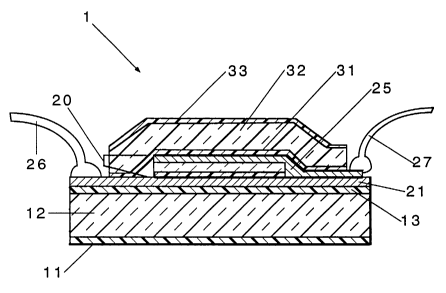
Fig. 1 is a cross-section of a representative embodiment of the device of the
present
invention.
Applicants' invention is an optoelectronic device comprising
(a) a transparent polymeric substrate bearing on at least one surface thereof
a
transparent polymerized organosilicon protective layer,
(b) a first electrode over the polymerized protective layer,
(c) an optoelectrically active film comprising an electroactive material, said
film
having a first side, which is in contact with the transparent electrode, and a
second side in
contact with a second electrode, wherein said first electrode is characterized
in that it allows
-2-
CA 02437472 2003-08-O1
WO 02/065558 PCT/US02/02886
light to pass to or from the optoelectrically active film. Preferably, the
device further
comprises additional protective packaging over the second electrode.
By "opto-electrically active filin" is meant a single layer or multi-layer
structure
which is capable of transporting charge and which emits light when charge is
transported
through the film andfor generates current when light is incident upon the
film. The film is
preferably made predominantly, or more preferably, entirely, from organic
materials.
"Electroactive material" and "optoelectronic material" are used synonymously
herein as describing the organic material possessing electronically
semiconductive
characteristics, which is capable of converting electrical charge to light, or
vice versa, or
being utilized as a semiconducting switch as in a field-effect transistor as
it is understood by
practitioners in the art.
The optoelectronic device includes photodiodes, thin film transistors,
photodetectors, and photovoltaics, but is preferably an electroluminescent
device.
The transparent polymeric substrate may be any optically clear polymeric
material.
Examples of suitable thermoplastic materials include polyethylene,
polypropylene,
polystyrene, polyvinylacetate, polyvinylalcohol, polyvinylacetal,
polymethacrylate ester,
polyacrylic acids, polyether, polyester, polycarbonate, cellulous resin,
polyacrylonitrile,
polyamide, polyimide, polyvinylchloride, fluorine containing resins, and
polysulfone.
Examples of thermosets are epoxy, diallyl carbonate, and urea melamine.
The thickness of the substrate is application dependent, but is preferably not
less
than about 0.1 mm, more preferably not less than about 0.3 mm, and most
preferably not
less than about 0.5 mm, and preferably not more than about 10 mm, more
preferably not
more than about 5 mm, and most preferably not more than about 2 mm.
Optionally, the
substrate may include an external protective coating to protect against
scratching of the
surface and similar properties on the opposite side of the substrate from the
surface bearing
the polymerized organosilicon protective layer. The abrasion resistant coating
may be any
such known coating. The external protective coating may be the same as the
polymerized
organosilicon protective layer.
The polymerized organosilicon protective layer is preferably formed by plasma
enhanced chemical vapor deposition, which initiates polymerization of an
organosilicon
compound in the presence of excess oxygen, as discussed in U.S. Patents
5,718,967 and
5,298,587. Starting materials may include silane, siloxane, or a silazane.
Examples of
silanes include dimethoxydimethylsilane, methyltrirnethoxysilane,
tetramethoxysilane,
_3_
CA 02437472 2003-08-O1
WO 02/065558 PCT/US02/02886
methyltriethoxysilane, diethoxydimethylsilane, methyltriethoxysilane,
triethoxyvinylsilane,
tetraethoxysilane, dimethoxymethylphenylsilane, phenyltrimethoxysilane, 3-
glycidyloxypropyltrimethoxysilane, 3-methacryloxypropyltrimethoxysilane,
diethoxymethylphenylsilane, tris(2-methoxyethoxy)vinylsilane,
phenyltriethoxysilane,
tetraethylorthosilane and dimethoxydiphenylsilane. Examples of siloxanes
include
tetramethyldisiloxane (TMDSO) and hexamethyldisiloxane. Examples of silazanes
include
hexamethylsilazane and tetramethylsilazane. The polymerized organosilicon
protective
layer preferably has the formula: S1O1.0-2.400.1-4.SH0.0-8.0~ more preferably
SiOl,o_2.4Co.2-z.4Ho.o-
a.o~ and most preferablySi01,8_2.4 Co.s-s.o ~d Ho.7a.o.
Preferably, the organosilicon protective layer includes an adhesion promoter
layer
adjacent to the substrate and between the substrate and the primary protective
layer. The
adhesion promoter layer may be any known suitable adhesion promoter but
preferably is a
first plasma polymerized organosilicon compound deposited on the surface of
the substrate
at a power level sufficient to create an interfacial chemical reaction for
adhesion and in the
25 substantial absence of oxygen. The protective coating layer is then a
second plasma
polymerized organosilicon compound (the primary protective layer) deposited on
the
surface of the adhesion layer at a power density from about 10~ J/kg to about
10$ J/kg, and
in the presence of a higher level of oxygen than in the step of applying the
adhesion
promoter.
Thus, according to a preferred embodiment, the surface of the substrate is
coated
first with an adhesion promoter layer, which is formed from the plasma
polymerization of
an organosilicon compound deposited on the surface of the substrate. The
plasma
polymerization of the organosilicon compound to produce the adhesion promoter
layer is
carried out at a sufficient power level to create an interfacial chemical
reaction for adhesion,
preferably, at a power level from about 5 x 10⁷ J/kg to about 5 x 10⁹ J/kg.
The adhesion
promoter layer is prepared in the absence or substantial absence of a carrier
gas, such as
oxygen. The term "substantial absence of oxygen" is used herein to mean that
the amount
of oxygen present in the plasma polymerization process is insufficient to
oxidize all the
silicon and carbon in the organosilicon compound. Similarly, the term
"stoichiometric
excess of oxygen" is used herein to mean that the total moles of oxygen
present is greater
than the total moles of the silicon and carbon in the organosilicon compound.
The thickness of the adhesion promoter layer is application dependent and is
preferably not less than about 50 A, snore preferably not less than about 500
t~, and most
-4-
CA 02437472 2003-08-O1
WO 02/065558 PCT/US02/02886
preferably not less than about 1000 ~, and preferably not more than about
10,0001, more
preferably not more than about 5000 ~, and most preferably not rnore than
about 2000 ~.
The adhesion promoter layer is then coated with a protective coating layer,
which is
a plasma polymerized organosilicon compound deposited on the surface of the
adhesion
promoter layer at a power density from about 106 J/kg to about 10$ J/kg, and
in the presence
of a higher level of oxygen than used to form the adhesion promoter layer.
Preferably, the
protective coating layer is formed in the presence of a stoichiometric excess
of oxygen.
The thickness of the protective coating for the substrate depends primarily on
the
properties of the 'coating, as well as the substrate, but in general, is
sufficiently thick to
impart solvent resistance to the substrate. Preferably, the coating thickness
is not less than
about 0.1 micron, more preferably not less than about 0.4 micron, and most
preferably not
less than about 0.8 micron, and not greater than about 10 microns, more
preferably not
greater than about 5 microns, and most preferably not greater than about 2
microns.
The protective layer structure, preferably, further comprises an SiOX layer,
which is
a plasma polymerized organosilicon compound, deposited on the surface of the
layer of the
protective coating layer, in the presence of a stoichiometric excess of
oxygen, and at a
power density of at least about twice, more preferably at least about 4 times,
and most
preferably at least about 6 times the power density used to form the
protective coating layer.
This layer is conveniently referred to as an SiOx layer. However, the SiOX
layer may also
contain hydrogen and carbon atoms. The thickness of the SiOx layer is
generally less than
the thickness of the protective coating layer, and is preferably not less than
about 0.01
micron, more preferably not less than about 0.02 micron, and most preferably
not less than
about 0.05 micron, and preferably not more than about 5 microns, more
preferably not more
than about 2 microns, and most preferably not more than about 1 micron.
It may be desirable to coat the adhesion promoter layer with alternating
layers of the
protective coating layer and the SiO~ layer. The ratio of the thicknesses of
the protective
I coating layers and the SiO;~ layers are preferably not less than about 1:1,
more preferably
not less than about 2:1, and preferably not greater than about 10:1, more
preferably not
greater than about 5:1.
The laminate is optically clear and comprises a substrate having a stress
optic
coefficient (SOC) in the range of from about -2000 to about +2500 Brewsters
and a Tg, as
determined by differential scanning calorimetry, preferably in the range of
from about
160°C to about 270°C. Preferably, the SOC of the substrate is
not less than about -1000,
-5-
CA 02437472 2003-08-O1
WO 02/065558 PCT/US02/02886
more preferably not less than about -500, and most preferably not less than
about -100, and
not greater than about 1000, more preferably not greater than about 500, and
most
preferably not greater than about 100 Brewsters. The Tg of the substrate is
preferably not
less than about 180°C, more preferably not less than about
190°C, and most preferably not
less than about 200°C, to not greater than about 250°C, more
preferably not greater than
about 240°C, and most preferably not greater than about 230°C.
The term "optically clear"
is used herein to mean that the substrate has a measured total light
transmission value
according to ASTM D-1003 of at least about 80 percent, preferably at least
about 85
percent.
The first electrode is preferably a transparent conductive material such as
ITO, but
may alternatively be a line, series of lines or grid of an opaque material, in
which case light
incident upon or emitted from the optoelectrically active layer is able to
pass around the
sides of the electrode, as discussed in U.S. Provisional Application Serial
No. 60/259,490,
filed January 3, 2001. When the electrode is made of ITO, the ITO can be vapor
deposited
onto the protective layer according to normal procedures for depositing ITO
onto substrates.
The optoelectrically active material is then applied over the electrode
according to
known procedures. These procedures include spin coating and other solvent
casting
methods. While the devices of this invention include those having
optoelectrically active
layers based on small organic molecules, see, for example, Tang and VanSlyke
in US Patent
4,885,221 and Tang in I~foYmatior~ Display, pp. 16-19, Oct. 1996, materials
such as
phenylenevinylene based polymers, thiophene based polymers, and fluorene based
polymers
are preferred. Most preferred are polymers, which comprise at least 5, more
preferably at
least 10, repeat units of the formula:
~ preferably having a polydispersity of less than 5, wherein Rl is
independently, in each
occurrence, Cl_2o hydrocarbyl or C1_20 hydrocarbyl containing one or more S,
N, O, P or Si
atoms, C4_16 hydrocaxbyl carbonyloxy, C4_ls aryl(trialkylsiloxy) or both R1
may form with
the 9-carbon on the fluorene ring a CS_zo ring stricture or a C4.~,o ring
structwe containing
one or more heteroatoms of S, N or O;
-6-
CA 02437472 2003-08-O1
WO 02/065558 PCT/US02/02886
R2 is independently, in each occurrence, Cl_2o hydrocarbyl, C1_20
hydrocarbyloxy,
Ci-ao thioether, Cl_zo hydrocarbylcarbonyloxy or cyano; and
a is independently, in each occurrence, 0 or 1. Preferably, substantially all
of these
repeat units are connected in the polymer chain via the 2 and 7 carbon atoms.
The polymers may be homopolymers, but more preferably, are copolymers of the
above repeat unit (or mer) with one or more additional conjugated mers.
Examples of these
other conjugated mers include mers derived from stilbenes or 1,4-dienes,
tertiary amines,
N,N,N',N'-tetraaryl-1,4-diaminobenzene, N,N,N',N'-tetraarylbenzidine, N-
substituted-
carbazoles, diarylsilanes, thiophenes, furans, pyrroles, polycyclic aromatics,
such as
acenaphthene, phenanthrene, anthracene, fluoranthene, pyrene, perylene,
nibrene, chrysene,
and corene; 5-membered heterocycles containing imine linkages, such as
oxazoles,
isoxazoles, N-substituted-imidazoles/pyrazoles, thiazoles/isothiazoles,
oxadiazoles, and N-
substituted-triazoles; six-membered heterocycles containing invne linkages,
such as
pyridines, pyridazines, pyrimidines, pyrazines, triazines, and tetrazenes;
benzo-fused
heterocycles containing imine linkages, such as benzoxazoles, benzothiazole,
benzimidazoles, quinolines, isoquinolines, cinnolines, quinazolines,
quinoxalines,
phthalazines, benzothiadiazoles, benzotriazines, phenazines, phenanthridines,
and,
acridines; and more complex mers, such as 1,4-tetrafluorophenylene, 1,4'-
octafluorobiphenylene, 1,4-cyanophenylene, 1,4-dicyanophenylene, and
CA 02437472 2003-08-O1
WO 02/065558 PCT/US02/02886
N~ o ~H o ~~ o ~~ o
o_o_
0
N~ N~SvN N// N
/ \\
N'X~N Nl X~N N/ X~N N/ ~N
U
X=O,S X=O,S X=O,S
N~N o Ph N~
N
~N
Ph
These polymeric materials may be used alone or in blends with other conjugated
polymers,
which, preferably, are also based on polyfluorene.
The optoelectricall,y active film may optionally comprise more than one layer.
For
instance, layers, which enhance charge injection andlor charge transport, may
be used with
one or both electrodes. Since holes are injected from the anode, the layer
next to the anode
needs to have the functionality of having holes injected into it and
transporting holes.
Similarly, the layer next to the cathode needs to have the functionality of
transporting
electrons. In many instances, the hole transporting layer or electron
transporting layer may
also act as the light emitting layer. In some instances, one layer can perform
the combined
functions of hole and electron transport, and light emission. The individual
layers of the
organic film may be all polymeric in naW re or combinations of films of
polymers and films
_g_
CA 02437472 2003-08-O1
WO 02/065558 PCT/US02/02886
of small molecules deposited by thermal evaporation. It is preferred that the
total thickness
of the organic film be less than 1000 nm. It is more preferred that the total
thickness be less
than 500 nm. It is most preferred that the total thickness be less than 300
nm.
The anode may be coated with a thin layer of a conducting substance to
facilitate
hole injection. Such substances include copper phthalocyanine, polyaniline and
poly(3,4-
ethylenedioxy-thiophene) (PEDOT); the last two in their conductive forms by
doping with a
strong organic acid, for example, poly(styrenesulfonic acid). It is preferred
that the
thickness of this layer be 200 nm or less; it is more preferred that the
thickness be 100 nm or
less. Alternatively, a more substantial separate hole-transporting layer is
used, the
polymeric arylamines described in U.S. Patent No. 5,929,194, may be used.
Other known
hole-conducting polymers, such as polyvinylcarbazole, may also be used. The
resistance of
this layer to erosion by the solution of the film, which is to be applied
next, is obviously
critical to the successful fabrication of multi-layer solution coated devices.
The thickness of
this layer may be 500 nm or less, preferably 300 nm or less, most preferably
150 nm or less.
Alternatively, the optional hole-transporting layer for these devices may be
selected from
among semi-conducting polymers, such as doped polyaniline, doped poly(3,4-
ethylene-
dioxythiophene), and doped polypyrrole. By "doping" is meant the blending of a
semiconducting polymer (such as emeraldiiie base of polyaniline and poly(3,4-
ethylene-
dioxythiophene) with an additive, which renders the resulting polymer
compositions more
conductive. Preferably, the conducting polymer is derived from blending
poly(3,4-
ethylene-dioxythiophene) with a polymeric acid. More preferably, the polymeric
acid
contains sulfonic acid groups, and is most preferably poly(styrenesulfonic
acid). Most
preferred are polymer compositions derived from blending poly(3,4-ethylene-
dioxythiophene) with at least two equvalents of poly(styrenesulfonic acid).
If an electron-transporting layer is used, it may be applied either by thermal
evaporation of love molecular weight materials or by solution coating of a
polymer with a
solvent that would not cause significant damage to the underlying film.
Examples of low
molecular weight materials include the metal complexes of 8-hydroxyquinoline
(as
described in Burrows, et al., Applied Physics Letters, Vol. 64, pp. 2718-2720
(1994));
metallic complexes of 10-hydroxybenzo(h)quinoliue (as described in Hamada, et
al.,
Chemistry Letters, pp. 906-906 (1993)); 1,3,4-oxadiazoles (as described in
Hamada, et al.,
OptoelectrorZics - Devices and Techsaologies, Vol. 7, pp. 83-93 (1992));
1,3,4-triazoles (as described in I~ido, et al., Clzer~aistry Letters, pp. 47-
48 (1996)); and
dicarboximides of perylene (as described in Yoshida, et al., Applied Physics
Letters,
-9-
CA 02437472 2003-08-O1
WO 02/065558 PCT/US02/02886
Vol. 69, pp. 734-736 (1996)). Polymeric electron transporting materials are
exemplified by
1,3,4-oxadiazole-containing polymers (as described in Li, et al., Jou~~,al of
Chemical
Society, pp. 2211-2212 (1995), and in Yang and Pei, Journal ofApplied Physics,
Vol. 77,
pp. 4807 to 4809 (1995)); 1,3,4-triazole-containing polymers (as described in
Strukelj, et
al., Science, Vol. 267, pp. 1969 to 1972 (1995)); quinoxaline-containing
polymers (as
described in Ya.mamoto, et al., Japan Journal. of Applied Physics, Vol. 33,
pp. L250 to L253
(1994), and in O'Brien, et al., Synthetic Metals, Vol. 76, pp. 105 to 108
(1996)); and cyano-
PPV (as described in Weaver, et al., Thin Solid Films, Vol. 273, pp. 39 to 47
(1996)). The
thickness of this layer may be 500 nm or less, preferably 300 nm or less, most
preferably
150 nm or less.
The metallic cathode may be deposited either by thermal evaporation or by
sputtering. The thickness of the cathode may be from 100 nm to 10,000 nm. The
preferred
metals are calcium, magnesium, indium, ytterbium, and aluminum. Alloys of
these metals
may also be used. Alloys of aluminum containing 1 to 5 percent of lithium and
alloys of
magnesium containing at least 80 percent of magnesium are preferred.
The EL devices of this invention emit light when subjected to an applied
voltage of
50 volt or less with luminance efficiency of at least 0.1 lumens/watt, but
which may be as
high as 2.5 lumens/watt.
The device may be further packaged and protected from the environment by
adhering a cover, such as is disclosed in WO 00/69002, to the substrate and
over the active
materials. An alternative protective package could include a flexible barrier
coated polymer
film. This barrier coated polymer film may be similar or the same as the
substrate bearing
the polymerized organosilicon protective barrier or may be any other siutable
material.
Referring now to Fig. 1, one sees a cross-section, not to scale, of a
representative
device 1 of this invention. This device comprises a substrate 12 having an
external
protective layer 11 on one side and the polymerized organosilicon protective
layer 13 on the
opposite side. On the polymerized organosalicon protective layer 13, the anode
21 is found.
The optoelectronic or optoelectrically active film 20 is located on the anode.
This film 20
comprises a hole transport layer 23 and a layer 24 of optoelectronic material.
Over film 20
is found the cathode 25. Connectors 26 and 27 connect the device to a power
source (for an
OLED device) or to a ciurent detector for a photodetector. This representative
device is
shown with complete packaging that, in this case, comprises an internal
barrier layer 31,
-10-
CA 02437472 2003-08-O1
WO 02/065558 PCT/US02/02886
which may be the same as or different from layer 13, a polymeric film 32, and
an optional
second external protective layer 33.
Ex_ arnnle
The PECVD coating chamber and all substrate handling is performed in a Class
10000
clean room. Prior to deposition, all interior components of the chamber are
cleaned to
minimize particle contamination of the deposited films. The base substrates
for the PLED
devices were 300 mm x 300 mm x 1.0 mm polycarbonate sheets purchased from the
Goodfellow Corporation. The sheets are fixtured in the plasma chamber by using
binder
clips and wire hangers. A single coating run is comprised of two sheets
suspended
vertically between the electrodes which are spaced at 25 cm. The substrates
are equidistant
from the electrode faces. The chamber is then evacuated to a base pressure of
approximately 1 mTorr before the start of the deposition sequence. An adhesion
layer is
deposited using a 16.5 standard cubic centimeters per minute (sccm) flow rate
of
tetramethyldisiloxane (TMDSO) which is controlled by an MKS Model 1152 vapor
flow
controller. A 40 kHz electric field is capacitively coupled to the electrodes
form an
Advanced Energy Model PE II power supply. The power loaded to the plasma
during the
deposition of the adhesion layer is 800 W. The chamber pressure is not
directly controlled
in this chamber, but is rather is determined by a balance of gas flow rate
into the chamber
and pumping speed of amused reactants and gaseous products generated as a
result of the
plasma process. The process pressure for the adhesion layer is around 4-6
mTorr. The
thickness of the deposited adhesion layer is approximately 100 ~, constituting
a deposition
time of 45 seconds. At this point, oxygen feed to the chamber is commenced at
40 sccm of
oxygen using an MKS Model 1160 mass flow controller. The flow of TMDSO is then
ramped from 16.5 sccm to 50 sccm over a 3 minute time span. At the completion
of this
2S ramp, the layer having the chemical composition in the range of
Si01,8_2.4Co.s-Z.oHo.7-a.o is
deposited fox 1 hour, which constitutes a thickness of approximately 2.5
microns. This
layer is also grown with an applied power of 800 W. The process pressure for
this layer is
approximately 9 mTorr. When the desired thickness is attained, the vapor feed
of TMDSO
is reduced to 16.5 sccm, and the flow of oxygen is increased to 195 sccm over
the time span
of approximately 10 seconds. The applied power is increased to 1500 W, and the
SiOx
layer is grown to a thickness of approximately 300 ~1 in a 3 minute deposition
time. When
this layer is complete, the applied power is turned off and all gas feeds are
ceased. The
chamber is then vented to atmospheric pressure and the substrates are removed.
After
cleaning the electrodes and inner chamber components, the system is ready for
another
-11-
CA 02437472 2003-08-O1
WO 02/065558 PCT/US02/02886
deposition. The anode made from indium tin oxide (ITO) is deposited over the
barrier layer
composition by standard plasma deposition process for ITO. Baytrori-PTM
polyethylene
dioxythiophene from Bayer Corp. is spin coated over the ITO and is allowed to
thoroughly
dry. A polyfluorene based light emitting polymer is spin coated over the
Baytron-P layer.
The coated substrate is inserted into the vacuum metallization system, which
operates at a
base pressure in the 10-7 Torr (mbar) range. In this chamber, the cathode is
deposited,
which consists of a thin layer of calcium followed by a thiclcer layer of
silver as a protective
overcoat. The device is now operational but is further encapsulated or
packaged to protect
the electroactive components from damage by environmental conditions and
handling. The
device so made was operational in air:
-12-