Note: Descriptions are shown in the official language in which they were submitted.
CA 02437793 2009-07-07
77496-156
AUTOMATIC WIRELESS SYNCHRONIZATION OF ELECTRONIC ARTICLE
SURVEILLANCE SYSTEMS
BACKGROUND OF THE INVENTION
Field of the Invention
This invention relates to the operation of multiple electronic article
surveillance (EAS) systems, and more particularly the wireless synchronization
of
EAS systems operating in the same vicinity of each other.
Description of the Related Art
EAS systems in close proximity often must be carefully synchronized
to avoid adverse interactions. There are several different levels of
synchronization
possible. The transmitter's carrier oscillator can be synchronized, or the
transmitter's modulating waveform can be synchronized. In more complex
systems, such as those sold by Sensormatic Electronics Corporation under the
trademark ULTRAMAX, the transmitter configuration sequence can be
synchronized between multiple systems.
U.S. Patent No. 6,201,469, issued March 13, 2001, by Sensormatic
Electronics Corporation, covers synchronization of the transmitter
configuration
sequence.
1
CA 02437793 2003-08-07
WO 02/063771 PCT/US02/02485
Synchronizing the transmitter sequence is important for EAS systems that are
in very close
proximity to each other such that their interrogation zones overlap. As
disclosed in that
application, the transmit burst timing is tied directly to the power line zero
crossing function,
for which the phase is manually adjusted.
There is a need for synchronizing the transmit carrier's modulating waveform
for
EAS systems in close proximity, even if their interrogation zones are not
overlapping. In
swept RF systems this means synchronizing the sweeping function between
multiple
transmitters. In pulsed systems, such as ULTRA*MAX, this means synchronizing
the
transmitter pulse function between multiple systems.
Pulsed EAS systems positioned within hundreds of feet of one another must have
their transmit burst timing precisely aligned or the transmitters will
interfere with one
another's receivers, decreasing sensitivity or causing false alarms. In prior
systems this has
been accomplished by using the three phases of the power line for
synchronization. Each
system is plugged into the 60 (or 50) hertz power system, which is divided
into three phases.
Each phase is a sinusoidal function nominally offset from one another by 1/180
of a second
(or 1/150 of a second for 50 hertz systems) apart. The zero crossing of the
power line is used
as a timing reference, assuming that this 1/180 second separation is correct.
However, due to
variations of loading conditions across the three phases of the power line,
often they are not
exactly spaced 1/180 seconds apart. This causes the systems to interfere with
each other,
which in turn causes a service call to local technicians. The technicians must
come and
manually adjust the timing of the systems. If loading conditions on the power
lines change,
the process repeats itself at great expense to the company.
Another problem with using the power line as a timing reference is that the
power line
is not necessarily sufficiently stable. In particular, the zero crossing has a
significant amount
of phase noise. This phase noise is translated directly to timing jitter on
the system
2
CA 02437793 2009-07-07
77496-156
transmitters. Since the phase noise on the three line phases may not be
correlated, the jitter experienced by multiple systems compounds the problem.
In swept RF systems whose interrogation zones overlap,
interference of the two transmit signals can cause decreased performance. In
the
worst case, one transmitter may be sweeping low while the other is high, and
visa
versa. The envelope of the two transmitters (i.e., the carrier's modulating
function)
must be synchronized for best performance.
Synchronization of adjacent EAS systems can be accomplished by
hardwiring the systems so that timing of each EAS system can be precisely
controlled. Hardwiring of adjacent EAS systems is not always feasible or cost
effective. Manual adjustment coupled to and power line zero crossings include
the limitations described hereinabove. A wireless, automatic method of
synchronizing the transmit carrier's modulating waveform for an EAS system is
needed.
BRIEF SUMMARY OF THE INVENTION
Some embodiments provide a distributed wireless phase locked loop
system for synchronizing the transmit carrier's modulating waveform, such as
the
transmitter pulse timing in a pulsed EAS system and the transmit sweeping
function for swept RF synchronization. To remove the effect of phase noise on
the power line signal, a phase locked loop is used to filter this signal. The
filtered
output is used as a reference to a second dependent phase locked loop tied to
a
numerically controlled oscillator and the received signal to provide a
distributed
phase looked loop algorithm that is wireless, and automatically synchronizes
adjacent EAS systems.
According to one aspect of the present invention, there is provided
apparatus for wireless synchronization of electronic article surveillance
systems,
reducing the need for manual adjustment of transmitter timing by continually
adapting and updating timing automatically to changing environmental
conditions,
comprising: a first phase locked loop including: means, responsive to a power
line
3
CA 02437793 2009-07-07
77496-156
zero crossing, for detecting a line phase error; a first numerically
controlled
oscillator responsive to said line phase error and to a crystal oscillator,
said first
numerically controlled oscillator and having a reference output, said
reference
output being an input to said line phase error means; and, a second phase
locked
loop including: means, responsive to a transmit signal from a first electronic
article
surveillance system, for detecting a transmit phase error; and, a second
numerically controlled oscillator responsive to said transmit phase error and
said
reference output; said second numerically controlled oscillator having a
synchronized transmit output, said synchronized transmit output being an input
to
said transmit phase error means; and, wherein said synchronized transmit
output
being usable as a trigger for synchronized transmission of a second electronic
article surveillance system.
According to another aspect of the present invention, there is
provided a method for wireless synchronization of electronic article
surveillance
systems, reducing the need for manual adjustment of transmitter timing by
continually adapting and updating timing automatically to changing
environmental
conditions, comprising: detecting a power line zero crossing and a reference
output from a first numerically controlled oscillator to provide a line phase
error
signal; said first numerically controlled oscillator receiving said line phase
error
signal and an oscillator signal and generating said reference output; and,
detecting a transmit signal from a first electronic article surveillance
system and a
synchronized transmit output from a second numerically controlled oscillator
to
provide a transmit phase error; said second numerically controlled oscillator
receiving said transmit phase error and said reference output and generating
said
synchronized transmit output, wherein said synchronized transmit output being
usable as a trigger for synchronized transmission of a second electronic
article
surveillance system.
According to still another aspect of the present invention, there is
provided an electronic article surveillance system incorporating wireless
synchronization of a plurality of electronic article surveillance systems,
reducing
the need for manual adjustment of transmitter timing by continually adapting
and
4
CA 02437793 2009-07-07
77496-156
updating timing automatically to changing environmental conditions,
comprising:
an electronic article surveillance transmitter and receiver and at least one
antenna
connected to the transmitter and receiver, said transmitter including: a first
phase
locked loop including: means, responsive to a power line zero crossing, for
detecting a line phase error; a first numerically controlled oscillator
responsive to
said line phase error and to a crystal oscillator, said first numerically
controlled
oscillator and having a reference output, said reference output being an input
to
said line phase error means; and, a second phase locked loop including: means,
responsive to a transmit signal from a first of a plurality of electronic
article
surveillance systems, for detecting a transmit phase error; and, a second
numerically controlled oscillator responsive to said transmit phase error;
said
second numerically controlled oscillator having a synchronized transmit
output,
said synchronized transmit output being an input to said transmit phase error
means; and, wherein said synchronized transmit output being usable as a
trigger
for synchronized transmission of a second of said plurality of electronic
article
surveillance systems.
4a
CA 02437793 2009-07-07
77496-156
Filtering of the line phase error where the first numerically controlled
oscillator is
responsive to a filtered line phase error and filtering the transmit phase
error where the
second numerically controlled oscillator is responsive to a filtered transmit
phase error can
also be implemented.
The first phase locked loop may further include a counter that is responsive
to the
crystal oscillator, and a readable capture register that is responsive to the
power line zero
crossing and to an output of the counter. The readable capture register output
is the line
phase error. A processor responsive to the power line zero crossing, to the
line phase error,
and to a power line phase locked loop interrupt can be used to select a value
for a
programmable period register. A comparator can be used for comparing the
output of the
counter and the value of the programmable period register. The comparator can
be used to
reset the counter and for sending the power line phase locked loop interrupt
to the processor.
The second phase locked loop can include a counter having an output and
comparators for comparing the counter output to each of four programmable
registers. The
comparators can generate four compare interrupts sent to the processor.
4b
CA 02437793 2003-08-07
WO 02/063771 PCT/US02/02485
Objectives, advantages, and applications of the present invention will be made
apparent by the following detailed description of embodiments of the
invention.
BRIEF DESCRIPTION OF THE SEVERAL VIEWS OF THE DRAWINGS
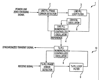
Figure 1 is a block diagram of one embodiment of the present invention.
Figure 2 is a block diagram of one embodiment of the numerically controlled
oscillator and phase error detector used for the power line phase locked loop.
Figure 3 is a plot of the output waveform of the numerically controlled
oscillator
shown in Fig 2.
Figure 4 is a block diagram of the numerically controlled oscillator for the
transmitter
phase locked loop.
Figure 5 is a timing diagram showing transmit pulses and the power line
voltage with
phases A, B, and C.
Figure 6 is a block diagram of one embodiment for the hardware of the receiver
section.
Figure 7 is a timing diagram showing transmit and receive windows.
Figure 8 is a flow chart showing the transmitter phase locked loop controller
while
unlocked.
Figure 9 is a flow chart showing the lock detection algorithm.
Figure 10 is a flow chart showing the transmitter phase locked loop antenna
combining algorithm.
DETAILED DESCRIPTION OF THE INVENTION
Referring to Fig. 1, one embodiment of the present invention is illustrated as
implemented in a pulsed EAS system and includes generally two phase locked
loops 1 and
5
CA 02437793 2003-08-07
WO 02/063771 PCT/US02/02485
10, which can be referred to as an outer or independent loop 1 and an inner or
dependent loop
10. In independent loop 1, the power line zero crossing signal from the power
line connected
to the EAS system is input to the line phase locked loop (PLL) error detector
2. The output
of line PLL error detector 2 is connected to line PLL filter 3, the output of
which is connected
to line numerically controlled oscillator (NCO) 4. Line NCO 4 is responsive to
the reference
frequency from crystal oscillator 6 and to the output of line PLL filter 3.
Crystal oscillator 6
includes any oscillator sufficiently stable to provide a suitable reference.
The output of line
NCO 4 is input to line PLL error detector 2, and is used as a reference for
transmit PLL NCO
8. In dependent loop 10, a received signal from the EAS system's receive
antenna, which is a
signal received from adjacent EAS systems, is input to a transmit PLL phase
error detector 7.
The output of transmit PLL error detector 7 is connected to transmit PLL
filter 9, the output
of which is connected to transmit PLL NCO 8. Transmit PLL NCO 8 is responsive
to the
reference from independent loop 1 and the output of transmit PLL filter 9. The
output of PLL
NCO 8 is input to transmit PLL error detector 7, and as the trigger for the
transmit burst. In
loops 1 and 10, in one embodiment for example, even numbered reference
numerals indicate
items that are preferably implemented in hardware and odd numbered reference
numerals
indicate items that are preferably implemented in software.
Referring to Fig. 2, one embodiment for the NCO and phase error detector for
the line
PLL is illustrated. The main components of this subsystem are the counter 12
and
comparator 14. Counter 12 increments up from zero by one on each clock input
from crystal
oscillator 6. The programmable period register 16 and the counter output are
inputs to the
comparator 14. When the two inputs are equal, the comparator 14 sends an
output to the
counter 12 to reset back to zero. The output waveform of the NCO is
illustrated in Fig 3 for
open loop operation (i.e., the period register 16 is not being updated by the
loop filter output).
The comparator 14 output is also sent as an interrupt to the microprocessor 19
to take its
6
CA 02437793 2003-08-07
WO 02/063771 PCT/US02/02485
action as loop filter. Finally, the capture register 18 serves as a phase
error detector. The
value of the counter 12 at the time the zero crossing event occurs is a
measure of phase error
between the NCO and the actual line voltage waveform.
Referring to Fig. 4, the NCO for the transmitter PLL is illustrated. The
"phase A",
"phase B", and "phase C" event times, as shown in Fig. 5 and fully described
below, are
determined by compare registers 20-23, comparators 24-27, and counter 28.
There are four
compare events for when the line period and transmit burst period are not
commensurate, and
when the transmit burst period is less than one-third the line period, as
fully explained below
in the transmitter PLL operation.
Referring back to Figs. 1 and 2, the following describes the power line phase
error
detector 2. As with any PLL, we assume that the actual power line frequency is
not too far
off from the nominal value (e.g., 60 Hz). This is in fact true, since the
power line frequency
is typically very accurate even thought it does exhibit considerable phase
noise. The power
line zero crossing signal triggers the capture register 18 to hold the current
contents of the
counter 12 and also generates an interrupt to the processor 19. The processor
19 responds
with its interrupt service routine. The interrupt service routine software
runs the control
update algorithm and the power line loop filter 3.
The current value of the programmable period register 18 is denoted p(n),
where (n) is
the line PLL sample index. The value of the capture register 18 at sample time
(n) is denoted
x(n). We assume that if x(n) > p(n)/2, then the zero crossing signal occurred
earlier than
expected, otherwise it occurred later than expected. In other words, the zero
crossing phase
error signal, denoted e(n), is expressed as
e(n) = x(n) - p(n),
if x(n) > p(n)/2, otherwise it is
e(n) = x(n).
7
CA 02437793 2003-08-07
WO 02/063771 PCT/US02/02485
The line PLL makes use of a combination proportional and integral controller,
where
the two controller outputs are summed together, this can be written as
c(n) = gp(n) + g;(n)
The proportional controller output is simply a gain (Al) times the phase
error, or gp = Al *
e(n). After experimenting with several integrator schemes, the integrator
chosen sums the
past controller output c(n-1) with a gain times the present phase error, or
g;(n) = c(n-1) + A2 * e(n).
This type of proportional controller yields good performance and is
computationally simple.
In order to prevent the magnitude of the proportional controller output from
getting too large
during a transient or unlocked period, a limiter is utilized on g;(n) .
The total controller output is therefore
c(n) = Al * e(n) + c(n-1) + A2 * e(n)
If the loop lock detector has determined the loop is locked, this total
controller output is
filtered with a short fir filter. (This filter is the only difference in the
PLL implementation in
the locked versus unlocked cases.) In either case, the nominal line period
length is added to
this value c(n), the value is limited to prevent the loop from locking to a
harmonic, and the
final value is written to the programmable period register 16.
The line PLL lock detector checks the magnitude of c(n) each line cycle. Each
time c(n)
is smaller than some threshold, a counter is incremented. If c(n) is larger
than the threshold,
the counter is decremented. If the counter gets above an experimentally
determined level, the
loop is considered locked. If it drops below another experimentally determined
level, it is
considered unlocked.
Referring again to Fig. 4, the transmitter PLL is considerably more complex
than the
line PLL. It is a distributed PLL, where multiple pulsed EAS systems, such as
ULTRA*MAX systems, in proximity to one another phase lock to each others'
transmit
8
CA 02437793 2003-08-07
WO 02/063771 PCT/US02/02485
signal. Each system has identical but separate control algorithms, i.e., there
is no master
system keeping time.
Referring to Fig. 5, all ULTRA*MAX systems adhere to a timing scheme which is
tied
to the power line frequency. For example, domestic systems using 60 Hz power
have a
transmitter burst repetition rate that is some submultiple of 180 Hz, e.g., 30
Hz, 45 Hz, 60 Hz,
or 90 Hz. This is based on the three phase implementation of the power line
distribution
system. Typical system timing is shown in Fig. 5 where the system is running
at 90 Hz
repetition rate. The basic time interval is the "line phase", which is the
power line period
divided by 3. The phases are called (arbitrarily) "A", "B", and "C". The
transmitter fires for
1.6 milliseconds at the beginning of one phase, then listens for a tag
response. During the
following phase the transmitter does not fire, but listens to the noise
environment. The
transmitter fires every other line phase. Other examples would be to fire
every third line
phase, every fourth line phase, or every sixth line phase. A line phase in
which the
transmitter fires is a "transmit phase", while a line phase in which the
transmitter does not
fire is a "noise average phase".
Referring to Fig. 6, each conventional ULTRA*MAX system implementing the
present
invention can use existing receiver hardware to look for adjacent system
transmitters. The
same receiver hardware is used to detect tags, so there is virtually no
additional hardware cost
incurred in an existing system to implement the present invention. There can
be four
transceiver (transmit and receive) antennas 31-34, and six passive antennas 35-
40, which are
combined 42, 43, into four analog front-end (AFE) channels 44-47. Note that
there can be
more receive antenna inputs than there are AFE channels. If this is the case,
the system
control software will interrogate the various receive antennas in a "round
robin" fashion. The
analog front-end channels 44-47 are multiplexed 48, sampled by an analog to
digital
converter (ADC) 49, and passed into the digital signal processing (DSP)
subsystem 50.
9
CA 02437793 2003-08-07
WO 02/063771 PCT/US02/02485
Referring also to Fig. 7, the software defines the combination of a transmit
phase and a
noise average phase, as defined above and shown in Fig. 5, as a "time slot".
The compare
events from the transmitter PLL NCO 8, and comparators 24-27 in Fig. 4,
generate interrupts
to the processor. These compare events indicate the beginning of the next line
phase. If the
new line phase is a transmit phase, then a transmit burst is started,
otherwise no transmit burst
is started. In a transmit phase, a 1.6 millisecond transmit burst is generated
at 51. At the end
of the burst, an interrupt is generated 52 which triggers the ADC circuitry 49
to begin
sampling the four analog front end channels 44-47, and pass the samples into
buffers in the
DSP memory 50. The ADC 49 continues to sample through the remainder of the
time slot
until the next transmit burst is to be generated (about 9.51 millisecond for a
60 Hz line
voltage). During this time a second compare event 53 will also occur, but this
corresponds to
the start of a noise average phase, so no transmit pulse is started. The ADC
49 samples the
receiver during this time so that adjacent system transmitters 54 can be
sensed.
There are many ways to implement the phase error detector for the transmitter
PLL. In
a white Gaussian noise environment, the optimum detector would be a bank of
quadrature
matched filters matched to the ULTRA*MAX transmitter signal. The peak output
in time
could be located and taken as the position of the adjacent systems'
transmitters. The
environment is not additive white Gaussian noise, but simple nonlinearities
could be added to
the filtering to achieve good performance. However, the computational
requirements of this
approach are very high. An alternative approach is an energy balancing scheme,
or
"early/late" phase error detector. In this approach the energy of the adjacent
systems'
transmitters is attempted to be kept balanced around the optimum center point
in time of
where the transmitters should be. Both the quadrature matched filter bank
approach and the
early/late detector approach have been analyzed and simulated. When the
adjacent system
signals are weak, the matched filter approach is far superior. However, when
the signals are
CA 02437793 2003-08-07
WO 02/063771 PCT/US02/02485
strong there is little difference in performance. Because the early/late
detector is so much
simpler, it is used for implementation of the auto-synchronization disclosed
herein.
Returning to Fig. 7, the six windows, denoted "window(O)" through "window(5)"
represent how the receive ADC samples are segmented for the purpose of
detecting the
energy-of adjacent system signals. Note that the boundary of window(2) and
window(3) is
precisely the center point of where the adjacent system transmit signals
should be 54. That is,
assuming the transmitter PLL is locked then half of the adjacent transmit
signal will be in
window(2) and half will be in window(3).
The first part of the transmit PLL phase error detector and loop controller is
to
calculate the energy in each of the windows for each of the receive antennas
connected to the
AFE channels 44-47. For shorthand notation, let (a) denote the antenna, (w)
denote the
window (0 through 5), and (m) is a sample time index. The energies calculated
on antenna
(a), for window (w) at sample time (m) are denoted Energy(a,w,m). The next
part of the
phase error detector is to sort, or rank, the energies from largest to
smallest. The sorted array
of energies are denoted RankEnergy(a,k,m), where the window index has been
changed to (k)
to indicate the new ordering. The mapping from the time ordered energies
Energy(a,w,m) to
the magnitude ordered energies RankEnergy(a,k,m) is given by RankIndex(a,k,m).
That is, if
window number 2 had the most energy, then
RankEnergy(a,0,m) = 2.
Some other statistics are also calculated for the transmitter PLL. The ratio
of energy
in the early window (window 2) to late energy (window 3) is defined as
EarlyLateRatio(a,m) = Energy(a,2,m) / Energy(a,3,m).
The ratio of the largest energy window to the third largest window energy is
defined as
SNR1(a,m) = RankEnergy(a,0,m) / RankEnergy(a,2,m).
11
CA 02437793 2003-08-07
WO 02/063771 PCT/US02/02485
When the transmit PLL is locked, all of the transmit energy will be in the two
center
windows. The third largest window is noise only, although it is the strongest
noise window.
The weakest noise window is RankEnergy(a,5,m).
The ratio of the largest energy window to the fourth largest window is denoted
SNR2(a,m) = RankEnergy(a,0,m) / RankEnergy(a,3,m).
When the PLL is not in lock, the transmit signal may be in up to three windows
simultaneously. In this case SNR2 is a ratio of the window with the most
transmit energy
present to the largest noise only window. The ratio of the largest energy
window to the
weakest energy window is denoted
SNR3(a,m) = RankEnergy(a,0,m) / RankEnergy(a,5,m).
Finally, the energies calculated in the six windows are averaged over time
using single-pole
low pass filters to produce estimates of the average energy in each window for
each antenna.
These average values are denoted,
EnergyLPF(a,w,m).
These values are used to detect changes in the environment.
Referring to Fig. 8, initially, in the acquisition mode, line PLL must first
acquire and
become locked. After the line PLL has become locked, then the transmit (TX)
PLL starts at
60. On each time slot, the acquisition mode TX PLL controller is run for each
receiver
antenna that has been sampled by the ADC 49 for that time slot. The software
first checks
for exceptional situations: no signal is present or too many signals are
present at 61. If
RankEnergy(a,0,m) is not (much greater than) RankEnergy(a,3,m), then the "no
signal"
integrator is incremented at 62, if RankEnergy(a,O,m) (is much greater than)
RankEnergy(a,3,m), then the "no signal" integrator is decremented at 63. If
the "no signal"
integrator exceeds a specified threshold on all of the sampled receive
antennas, then the
system inserts a forced noise average following the current time slot. This
makes the
12
CA 02437793 2003-08-07
WO 02/063771 PCT/US02/02485
transmitter skip two line phases, instead of just one. The result is that any
adjacent systems
that were transmitting simultaneously (and thus cannot be seen by the receive
antennas) are
now transmitting one line phase off (and thus can be seen by the receive
antennas). If there
are too many signals, i.e., the systems see multiple transmit signals, which
are not
synchronized, the system can be locked to the highest signal. After this, the
software checks
two conditions to determine whether it should run high (coarse), medium, or
low (fine) gain
acquisition controllers.
If RankIndex(a,1,m) is not equal to window(0) or window(1) at 64, then the
coarse
gain controller is selected at 65. The coarse gain controller uses the
equation:
C(a,m) = [2=RankIndex(a,0,m) - 5 ] .10000,
where C(a,m) is the control value calculated from antenna (a) on the (m)t'
timeslot. This
control value is used to update the TX NCO compare registers 20-23, shown in
Fig. 4. This
control value has a maximum value of 50000 and a minimum value of -50000.
Since the
crystal oscillator driving the counter is 40 Mhz, these values correspond to
+/- 50000/40e6 =
+/- 1.25 milliseconds of time shift for the transmitter NCO compare events.
If RankIndex(a, l,m) is equal to window(0) or window(1) at 64, and window(2)
is not
approximately equal to window(3) at 66, then the medium gain controller is
selected at 67.
The medium gain controller uses the equation:
C(a,m) = [2-RankIndex(a,0,m) - 5 ] .2000.
This control value has a maximum value of 5000 and a minimum value of-5000.
These
values correspond to +/- 2000/40e6 =+/- 250 microseconds of time shift for the
transmitter
NCO compare events.
If RankIndex(a,1,m) is equal to window(0) or window(1) at 64, and window(2) is
approximately equal to window(3) at 66, then the fine gain controller is
selected at 68. The
fine gain controller uses the equation:
13
CA 02437793 2003-08-07
WO 02/063771 PCT/US02/02485
C(a,m) = sign(Energy(a,3,m) - Energy(a,2,m) ) =500.
This control value has a maximum value of 500 and a minimum value of-500.
These values
correspond to +/- 500/40e6 =+/- 12.5 microseconds of time shift for the
transmitter NCO
compare events.
If the high or medium gain controllers are run, then the lock integrator is
reset to zero
at 65 or 67, respectively. Otherwise, when the low gain controller is run at
68, the lock
detection routine is called at 69.
Referring to Fig. 9, the lock detection algorithm is called at 69. The lock
detection
algorithm is run for each antenna that has been sampled by one of the four AFE
channels 44-
47, as shown in Fig. 6 (i.e., if an antenna is not being received on by an AFE
channel, then
the TX PLL does not run on that antenna). The first section of the algorithm
sets four flags
that collectively give an indication of how well the system is synchronized.
The
EarlyLateBalanced flag is set at 70 if Energy(a,2,m) and Energy(a,3,m) are
within 3dB of
each other at 71, or else cleared at 72. The EarlyLateBiggest flag is set at
73 if
RankIndex(a,0,m) is equal to 2 or 3 at 74, or else cleared at 75. The
EarlyLate2ndBiggest
flag is set at 76 if RankIndex(a, l,m) is equal to 2 or 3 at 77, or else
cleared at 78. The
MostIn2Windows flag is set at 79 if RankEnergy(a, l,m) is much larger than
RankEnergy(a,2,m) at 80, or else cleared at 81.
Next at 82, the flags are combined together by the equation:
Index = 8 x EarlyLateBalanced + 4 x EarlyLate2ndBiggest +
2 x EarlyLateBiggest + Mostln2Windows,
and used as an index into a "lock integrator update" table at 83. The "lock
integrator
update" table is shown in the following table.
14
CA 02437793 2003-08-07
WO 02/063771 PCT/US02/02485
Index Status Integrator Update
0 Timing is way off -1024
1 Timing is way off -1024
2 Timing is getting close +4
3 Timing is getting close +4
4 Timing is getting close +4
Timing is getting close +4
6 Timing is getting very close +32
7 Timing is getting very close +32
8 Timing is way off -1024
9 iming is way off -1024
Timing is getting very close +32
11 Timing is getting very close +32
12 Timing is getting very close +32
13 Timing is getting very close +32
14 Timing is getting very close +32
Timing is locked +128
The integrator update from the "lock integrator update" table is added to the
integrator at 84.
The integrator is limited between 0 and MaxLocklntegrator, and nominally set
to 16384, at
5 85. To provide hysteresis, there are two lock thresholds for the integrator.
LowLockThreshold, nominally set to 8192, is set at 86 when the loop is locked
at 87.
HighLockThreshold, nominally set to 12288, is set at 88 when the loop is
unlocked at 87.
When the integrator exceeds the LockThreshold at 89 the lock status is set to
"locked" at 90.
When the integrator does not exceed the LockThreshold at 89 the lock
integrator is reset at 91
10 and the lock status is set to "unlocked" at 92.
The locked mode controller uses the equation
C(a,m) = sign(Energy(a,3,m) - Energy(a,2,m) ) -100.
This control value has a maximum value of 100 and a minimum value of -100.
These values
correspond to +/- 100/40e6 =+/- 2.5 microseconds of time shift for the
transmitter NCO
15 compare events.
On any given time slot, up to four receive antennas 31-40 may have been
sampled by
the DSP 50, as shown in Fig 6. Likewise, these same receive antennas would
have the Tx
CA 02437793 2003-08-07
WO 02/063771 PCT/US02/02485
PLL phase error detection and loop controller run on their sampled receive
data. Given that
the different receive antennas will have different noise characteristics and
will receive
adjacent system transmit signals with different strengths, the question is:
how do we combine
their phase detector/loop controller outputs?
If one were to devise criteria of goodness for the antenna combiner it may (or
it may
not) be possible to analytically derive an optimum combiner. Of course, this
combiner would
only be optimum for the criteria stated and assumptions used. If the
environmental
assumptions turned out to be inaccurate, there is little reason to believe the
solution would
still be optimum. Indeed, if the methods used are not robust, the resulting
combiner could be
very poor if the true system deviated from the model used. Also, the original
criteria may not
capture all of the qualities we want in the combiner.
It is important to realize what we have is a problem in antenna diversity
combining.
Considerable theoretical work and system implementation have been done in the
fields of
detection and estimation on antennas combining. Any of these results could be
adapted to
our approach. A commonly used "suboptimum" approach is choosing the antenna
with the
highest signal to noise ratio, and using this one all by itself. This method
is suboptimum in
performance, but is far less complex than the optimum combiner, which is why
it is used so
often. It turns out that in reasonably high SNR environments, the performance
difference is
usually quite small.
Referring to Fig. 10, one embodiment for the antenna-combining algorithm is
illustrated, starting at 100. If none of the individual receive antennas are
locked, the antenna
combiner is set to unlocked at 101. Next, if the combiner is locked at 102 it
ranks all of the
locked antennas, which were sampled in this time slot, according to SNR1, at
103. Otherwise
(if the combiner is not locked) all of the receive antennas which were sampled
this time slot
are ranked by SNR1, at 104. Following this ranking procedure, the algorithm
looks for the
16
CA 02437793 2003-08-07
WO 02/063771 PCT/US02/02485
highest ranked receive antenna with SNR2 greater than 20dB at 105. If such an
antenna is
found at 106, it is selected as the antenna with which to synchronize at 107,
and the phase of
transmitter PLL is adjusted accordingly. If no such antenna is found, the
combiner does not
update the Tx PLL phase at all at 108. The lock status of the combiner is set
to the lock
status of the selected antenna at 109.
The system can handle exceptional situations in operation. One problem
encountered is
that all EAS systems in proximity to one another may not be running off of the
same power
line frequency. This is the case if some stores within a mall are running off
of a generator,
while others are running off of different generators or the power line. In
this situation, there
will be a frequency offset between the transmitter repetition rates that must
be tracked by the
TX PLL. For example, one set of systems may be running at 90.1 Hz repetition
rate, while
another set may be running at 89.8 Hz repetition rate. This frequency offset
must be tracked
out by the TX PLL.
Two solutions are possible. First, the controller's gain can be increased so
that the lock
bandwidth of the PLL is high enough. However, increasing the PLL's bandwidth
in this way
also increases the steady state jitter due to noise. The second approach is to
increase the order
of the PLL, i.e., adding an integral term in the controller to track the
frequency offset.
Another exceptional situation occurs when the transmit PLL is unable to lock.
Perhaps it can see the other system's transmitters (sometimes), but due to
excessive noise it is
not able to achieve lock. Tag signals also may be affecting the energy content
in many of the
synohronization windows. Several options are available. First, have the
antenna combiner
criteria select antennas that see little or no tag signal or interfering
noise. Second, the
transmitter can occasionally be shut off to remove the tag signal or
transmitter induced noise.
Third, use a comb notch filter (ring down canceller) to remove stationary tags
in the
interrogation zone.
17
CA 02437793 2003-08-07
WO 02/063771 PCT/US02/02485
It is to be understood that variations and modifications of the present
invention can be
made without departing from the scope of the invention. It is also to be
understood that the
scope of the invention is not to be interpreted as limited to the specific
embodiments
disclosed herein, but only in accordance with the appended claims when read in
light of the
forgoing disclosure.
18