Note: Descriptions are shown in the official language in which they were submitted.
CA 02437815 2003-08-07
"Circuit for Processing Data"
The present invention relates to a circuit for processing data, including a
chip having at
" least two registers.
Circuits for processing data that include a chip having at least two registers
are sufficiently
well-known. Software for the search of data combined to form a database is
also known, in
which the data is generally composed of individual characters. This search is
generally
implemented through the sequential processing of a program with a commonly
used
computer.
Such a software implementation is particularly problematic to the effect that
even in a very
rapid clock cycle of the processor, the sequential processing of the required
commands of
such a program requires a very long total time.
The present invention is based on the task of specifying a circuit for
processing data, in
which the search of a database is chronologically optimized.
This aforementioned task is achieved according to the present invention
through a circuit
for processing data having the features of Patent Claim 1. Accordingly, the
circuit in
question for processing data is designed and developed such that rules for the
search of
data combined to form a database are filed in the registers and that the rules
are
substantially simultaneously processable.
In a manner according to the present invention, it was initially recognized
that, in a
departure from previous practice, a search of data combined to form a database
need not
be implemented through software but that a substantially faster search may be
achieved if
the search is implemented through hardware. In a further manner according to
the present
invention, it was then realized that the rules that define the search pattern,
according to
which the database is supposed to be searched, must be filed in registers, and
that the
rules must be processable substantially simultaneously and not sequentially,
for example.
In the process, the type of data involved is irrelevant. For example, the use
of the circuit in
intelligent search engines for the Internet is conceivable. Indeed, even very
different
applications are possible, for example in the field of the military industry
in collecting and
analyzing data. The circuit according to the present invention is certainly
suitable in a
CA 02437815 2003-08-07
2
particularly advantageous manner for use in different areas of molecular
biology, for
example, in the search for gene motifs or protein sequences. Through the
substantially
simultaneous processing of the rules, the speed of the search for every single
piece of data
may be increased considerably.
With regard to a particularly fast search of the data, the rules may be
processed within one
cycle or several cycles.
With respect to a detection of particularly critical and complex search
patterns, the rules
may include logical expressions and/or field definitions and/or wildcard
functions, in which
the wildcard function facilitates the generation of an output signal for every
single
character. Here, aside from individual characters, the search patterns may
also include
character combinations, for example, whole words and/or figures. In addition,
or
alternatively, the rules may also contain regular expression functions. In
logical
expressions, OR and AND/NOT operations would be particularly simple to
implement.
It would be of further advantage if the rules for searching the database were
to be filed in
encoded form in the registers. The registers may then exhibit a width of 2"-
bit. This would
make the implementation and detection of complex search patterns particularly
simple.
Within the scope of a particularly compact embodiment, the data of the
database could be
filed in a data storage device. In a particularly simple embodiment, this data
storage device
could be executed as RAM or FIFO.
In order to make a search of the data particularly simple, at least one data
register may be
positioned on the chip. Here, the data of the database, preferably from the
data storage
device, may be pushed intothe data register(s), which could be 2"-bit wide in
accordance
with the number of characters. The data of the database may then be pushed in
succession into and/or through the data register.
With respect to a particularly simple, and above all, optimized search, the
number of the
data register may be the same as the number of the register in which the rules
for
searching the database are filed, as a result of which, in a particularly
simple manner, the
processing of all the rules takes place in parallel and within one cycle. The
parallelity of the
circuit arrangement would then be two-dimensional, as it were. For one thing,
a window
CA 02437815 2003-08-07
3
would be opened up, in which the comparison of all the character or character
combination
positions of the data segment would be simultaneously facilitated, and, for
another, the
different characters or character combinations defined by the rules could be
detected for
each character or character combination position.
With respect to a once again very simple embodiment, the data could be encoded
using at
least one encoder. In this connection, the data could be encoded into a 2"-bit
code using
the encoder or the encoders. The encoding of the data to be searched would
facilitate a
particularly simple comparison between the data and the rules, thereby making
possible a
particularly fast detection of complex search patterns within one cycle.
With respect to a once again chronologically optimized embodiment, the
registers could be
comparable with data from the data registers) using one or several
comparator(s). The
comparator(s) could then, if necessary, compare the encoded rules and the
encoded data
bit for bit and, in the event of match, would generate an output signal in one
bit.
Alternatively, it would also be possible for the comparison of the individual
bits to be
implemented using AND gates.
Within the scope of a particularly simple embodiment of the chip, one
register, one data
register, one encoder and one comparator each may be combined to form an
individual
character element. Alternatively, an individual character element could also
exhibit only
one register, one data register, and one comparator. An encoder may then be
connected to
the individual character elements in order to encode the data before they are
pushed into
the data register.
With regard to a particularly functional arrangement, the individual character
elements
could be positioned in a parallel connection and preferably also on the chip.
This would
result in an uncomplicated circuit arrangement since most of the signals cycle
through the
circuit in a pipeline-like manner. The size of the simultaneously searchable
data segment -
or of the window in which the comparison of all character positions of the
data segment
would be simultaneously possible -- would then be defined through the number
of the
individual character elements connected in parallel.
CA 02437815 2003-08-07
4
The output signals of the comparators could then be added up using an adder.
Because of
this, it would be possible to make a statement as to what extent the searched
data
corresponds to the data being sought.
With respect to a particularly functional embodiment, the adder could be
created from
cascaded modules, in particularly from adders and/or adder registers. This
would facilitate,
in a particularly simple manner, adding a plurality of output signals from
comparators, in
which the number of the characters or character combinations to be compared
would not
be limited by the physical limitations of an individual adder.
Within the scope of a particularly variable search of the data, the output
signal of the adder
could be comparable with a threshold value using a component executing a
comparing
operation, for example, a comparator. The output signal of the adder could in
a particularly
advantageous manner be an n-bit word. In this connection, the threshold value
could be
variably specifiable within the scope of a particularly flexible embodiment,
and could be
configured such that, for instance, it specifies the percentage with which the
data searched
within the current cycle corresponds to the data sought.
If the threshold value is exceeded, the memory address of the detected data
and/or the
detected data may be output into a result register using an address pointer.
The address
pointer would accordingly track down in the data storage device the addresses
of the data
found in the data registers within the current cycle.
With respect to a possible further processing of the data, the output signal
of the adder
could be allocated to the address of the detected data in the data storage
device and/or to
the data and or may be output into the result register. It would consequently
even make it
possible, for instance, to further limit an already conducted search such that
only output
signals that exceed a further threshold value are taken into account.
With respect to a particularly user-friendly embodiment, a host computer may
be connected
to the circuit and/or to the chip using an interface. Using the host computer,
the rules for
searching the data may then be read into the register and/or the data could be
read into the
data storage device, for example. Alternatively, or in addition, the address
of the detected
data and/or the detected data, as well as the output signal of the adder, is
retrievable using
the host computer. The host computer here could be a standard PC.
CA 02437815 2003-08-07
With respect to a particularly compact embodiment, the chip and/or the data
storage device
and/or the address pointer and/or the result register and/or the interface
could be
positioned on at least one printed circuit board. However, it would also be
possible to
connect several chips and/or several data storage devices to one another
and/or to
position these on a printed circuit board. Alternatively hereto, the data
storage device
and/or the address pointer and/or the result register and/or the interface
could also be
positioned on the chip.
In order to once again achieve the optimization of the processing speed and to
deal with
the limitation of the bandwidth of the bus connecting the circuit, the data
may be retrieved
in parallel from the data storage device. The parallel structure could, in the
process, be
implemented in the data storage device and/or on the printed circuit board.
The data could
then be retrieved in parallel, for example, from the data storage device, as a
result of which
the speed of the retrieval would increase. Using a multiplexer integrated in
the data storage
device and/or on the chip and/or the printed circuit board, the data may be
merged and
then pushed into the data register. In this case, the number of input contacts
would
increase by the parallelity factor but the required bandwidth would diminish
by the same
factor.
There are now different possibilities for developing and enhancing the
teaching of the
present invention in an advantageous manner. In this regard, reference is
made, with the
help of the drawing, to the patent claims subordinate to Patent Claim 1 and to
the following
explanation of preferred exemplary embodiments of the circuit according to the
present
invention for processing data. In connection with the explanation of the
preferred
exemplary embodiments of the circuit according to the present invention, with
the help of
the drawing, preferred embodiments and enhancements of the teaching will also
be
explained in general. The drawing shows
Figure 1 in a schematic representation, an exempbry embodiment of a circuit
according to the present invention for processing data,
Figure 2 in a schematic representation, a further exemplary embodiment of a
circuit
according to the present invention
CA 02437815 2003-08-07
6
Figure 3 a schematic representation of the functional sequences in the circuit
according to the present invention
Figure 4 in a schematic representation, an individual character element of the
circuit
according to the present invention from Figure 1,
Figure 5 in a schematic representation, an individual character element of the
circuit
according to the present invention from Figure 2, and
Figure 6 in a schematic representation, a possible configuration of the
circuit
according to the present invention.
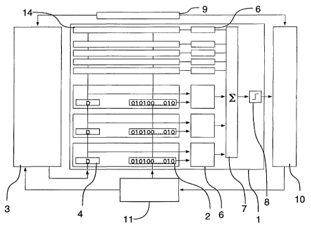
Figures 1 and 2 each show an exemplary embodiment of a circuit for processing
data,
including a chip 1 with 32 registers 2 - not shown completely here.
In a manner according to the present invention, rules for searching data
combined to form
a database are filed in registers 2 and the rules are simultaneously
processable.
The rules defining the search pattern are, in the exemplary embodiments,
logical
expressions as well as field definitions and wildcard functions. In this
exemplary
embodiment, the logical expressions include OR operations and AND-NOT
operations. The
rules for searching the database are filed in encoded form in registers 2, in
which the code
shown in Figures 1 and 2 correspond to the logical expression "B or W or Y".
The data of the database is filed in a data storage device 3. Data storage
device 3 is
executed as RAM in the exemplary embodiments.
Data registers 4 are positioned on chip 1, in which the data of the database
can be pushed
from data storage device 3. The number of data registers 4 is the same as the
number of
registers 2 in which the rules for searching the data are filed. This means
that 32 character-
long data records may be compared per cycle with the rules.
In the exemplary embodiment of Figure 2, the data is encoded using encoder 5.
This
involves n/2" encoders, which encode the data into an n-bit code. The data
will then be
CA 02437815 2003-08-07
7
compared bit for bit with the rules in registers 2 using comparators 6 and an
output signal is
generated in the event of a match.
In each case, one register 2, one data register 4, one comparator 6, and in
the exemplary
embodiment of Figure 2, one encoder 5, are combined to form an individual
character
element 14, 14'. The individual character elements 14, 14' are connected in
parallel, and
moreover, positioned parallel to each another on chip 1.
The output signals of comparators 6 are added up using an adder 7 and the
output signal
of adder 7 - in this case a 4-bit word - is compared with a threshold value
using a
component 8 executing a comparing operation. The threshold value gives the
possibility of
making an assessment as to the extent that the data should correspond to the
data sought,
and is variably specifiable by a user.
If the threshold value is exceeded, the address of the detected data in data
storage device
3 is filed using an address pointer 9 in a result register 10.
The functional sequences of the circuit are illustrated in Figure 3. The
searching of the data
takes place through successive pushing of the data through the data register
and
comparing the data with the search pattern specified by the rules. The output
signal of the
comparators shows whether the character examined matches the rule. The sum of
the
output signals is a measure of the conformity of the data searched with the
data sought,
since it shows how many characters match the search pattern. If the matches
vary in
degree, a trigger signal for storing the address of the detected data may be
generated
through a comparison with a variable threshold value.
Figures 4 and 5 schematically show the structure of an individual character
element 14, 14'
of the exemplary embodiments of Figure 1 and of Figure 2. In individual
character elements
14, 14', one register 2, one data register 4, as well as one comparator 6 are
combined,
while one encoder 5 is combined in the exemplary embodiment of Figure 2. The
individual
character elements 14, 14' are positioned in parallel and connected in
parallel to each other
on chip 1.
Figure 6 shows a printed circuit board, on 13, on which chip 1, data storage
device 3 and
an interface 10 are positioned. A host computer 12 - here a standard PC - may
be
CA 02437815 2003-08-07
8
connected to the circuit using interface 11. Using host computer 12, the rules
for searching
the data are initially read into register 2 and then the data into data
storage device 3. In
addition, using host computer 12, the threshold value is specified and the
address of the
detected data is retrieved from result register 10, and the detected data is
retrieved from
data storage device 3.
With respect to other details, reference is made to the general description to
avoid
repetitions.
Finally, it should be expressly indicated that the aforementioned described
exemplary
embodiments serve only to discuss the claimed teaching in detail, but that
these are not
restricted to the exemplary embodiments.